

Page 1

DFBM-NW726-DT0R
Data sheet
BLE Module
DFBM-NW726-DT0R
A Bluetooth Low Energy module with Antenna
on Package.
Preliminary Data Sheet Sheet 1 of 23 March 8, 2018
Proprietary Information and Specifications are Subject to Change
Page 2

DFBM-NW726-DT0R
Contents
1. Features .................................................................................................................................................4
1-1. General...............................................................................................................................................4
1-2. Bluetooth............................................................................................................................................4
2. Block Diagram......................................................................................................................................5
2-1. Use Antenna on Package ..................................................................................................................5
2-2. Use RF connector or External Antenna...........................................................................................5
3. General Specification...........................................................................................................................6
4. Electrical Characteristics......................................................................................................................7
4-1. Absolute Maximum Rating...............................................................................................................7
4-2. Recommended Operating Conditions & Power Consumption ......................................................7
5. RF Characteristics.................................................................................................................................8
5-1. Bluetooth RF characteristics ............................................................................................................8
5-2. Antenna characteristics.....................................................................................................................8
6. Pin Description .....................................................................................................................................9
7. Reference Circuit................................................................................................................................12
7-1. Use Antenna on Package ................................................................................................................12
7-2. Use RF connector or External Antenna.........................................................................................13
8. Module Dimensions (mm).................................................................................................................14
9. Recommend Soldering Conditions....................................................................................................16
10. Layout Guide (mm)............................................................................................................................17
10-1. Use Antenna on Package..............................................................................................................17
10-2. Use RF connector or External Antenna.......................................................................................17
11. Recommended Stencil Aperture........................................................................................................18
12. Packages..............................................................................................................................................20
12-1. Tape and Reel Specification.........................................................................................................20
12-2. Storage Specification....................................................................................................................21
13. Required End Product Labeling.........................................................................................................22
14. Manual Information to the End User.................................................................................................22
15. Federal Communications Commission (FCC) Statement................................................................22
Preliminary Data Sheet Sheet 2 of 23 March 8, 2018
Proprietary Information and Specifications are Subject to Change
Page 3
DFBM-NW726-DT0R
Recommended
Revision History
Rev. Date Reason of change Maker Approval
S04L 2018/9/03 Update FCC label Sog Sog
S04L 2018/8/24 Update NCC,EU message Sog Sog
S03L 2018/7/25 Update Bluetooth LE Version Sog Sog
S03 2018/06/13 Modify Delta Logo Sally Sally
S02 2018/03/08 Modify baking time Sally Sally
S01 2018/01/22 Update FCC / NCC / TELEC Certification Number Ryan Josh
1. Modify description in 6.Pin Description section
Pin3 P0.20 / TRACECLK
Pin5 P0.18 / TRACEDATA[0] / SWO
Pin11 P0.16 / TRACEDATA[1]
0.6 2018/01/10
0.5 2017/12/14 Certification based on BT4.2 Ryan Josh
0.4 2017/12/08 Modify Laser marking information Ryan Josh
0.3 2017/11/07 Update Package information Ryan Josh
0.2 2017/10/20 Modify ESD (HBM/CDM) specification Ryan Josh
0.1 2017/07/03 Initial release Ryan Josh
Pin13 P0.15 / TRACEDATA[2]
Ryan Josh
Pin15 SWDIO, remove reset description
Pin16 P0.14 / TRACEDATA[3]
2.Update detail dimension of footprint in 11.
Stencil Aperture section
3.Modify C3 from 10UF to NC in 7.Reference Design section
Preliminary Data Sheet Sheet 3 of 23 March 8, 2018
Proprietary Information and Specifications are Subject to Change
Page 4

DFBM-NW726-DT0R
T
DFBM-NW726-DT0R
BLE Module with Antenna on Package
his document describes the DFBM-NW726-DT0R wireless BLE module hardware specification. The
modules provide cost effective, low power, and flexible platform to add BLE for embedded devices for
a variety of applications, such as wireless sensors and thermostats. It uses BLE SoC, which integrating the
2.4GHz transceiver, a 32 bit ARM® Cortex M4F CPU,flash memory, and analog and digital peripherals.
1. Features
1-1. General
BLE chip with a single chip antenna or an external RF connector
Integrate a 32 bitARM® Cortex M4F CPU,512KB flash memory and 64KB RAM
12-bit 200kspc ADC - 8 configurable channels with programmable gain
30 General Purpose I/O Pins
Two-wire Master (I2C compatible) support 100K bps and 400K bps
UART baud rate up to 921600 bps
SPI bit rate up to 4M bps
Quadrature Decoder (QDEC)
LGA 48 pin package
Dimension 6.5mm(L) x 6.5mm(W) x 1.5 mm(H)
RoHS compliant
1-2. Bluetooth
Bluetooth 4.2/5 specification compliant
AES HW encryption
Preliminary Data Sheet Sheet 4 of 23 March 8, 2018
Proprietary Information and Specifications are Subject to Change
Page 5
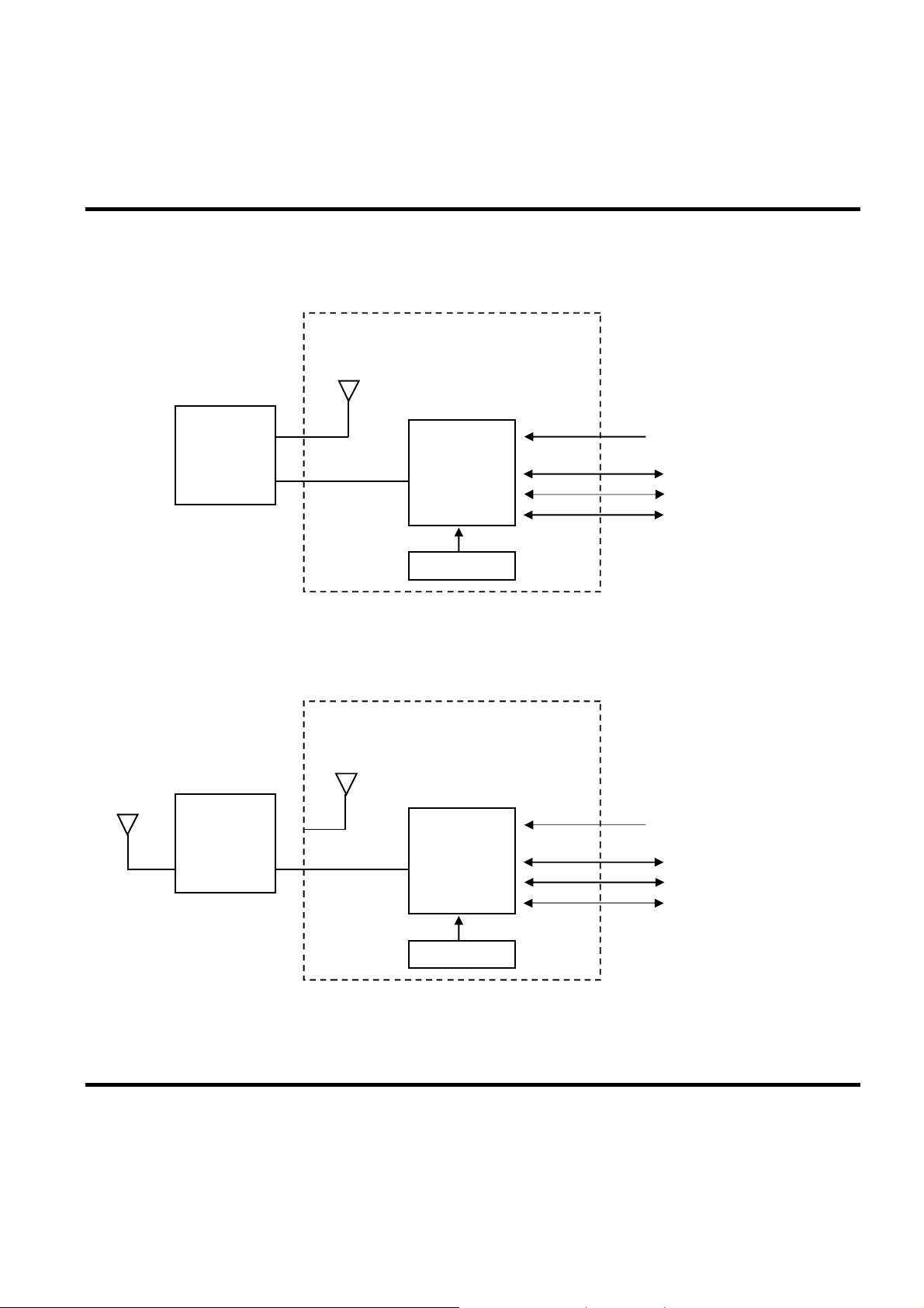
2. Block Diagram
SOC
SOC
2-1. Use Antenna on Package
Bluetooth ANT
On Package
DFBM-NW726-DT0R
Matching
Network
(Optional)
Figure 2-1. DFBM-NW726-DT0R Block Diagram (AOP)
Bluetooth
32MHz Crystal
2-2. Use RF connector or External Antenna
Bluetooth ANT
On Package
External Antenna
Matching
Network
(Optional)
Bluetooth
VDD: 1.7V ~ 3.6V
UART/SPI/I2C
GPIO
ADC
VDD: 1.7V ~ 3.6V
UART/SPI/I2C
GPIO
ADC
32MHz Crystal
Figure 2-2. DFBM-NW726-DT0R Block Diagram (External RF)
Preliminary Data Sheet Sheet 5 of 23 March 8, 2018
Proprietary Information and Specifications are Subject to Change
Page 6
DFBM-NW726-DT0R
3. General Specification
MCU ARM® Cortex®-M4 32-bit processor with FPU, 64MHz
Standard Bluetooth: V4.2 / Bluetooth:V5.0
Frequency 2.402 ~ 2.48 GHz
Modulation GFSK
Data Rate BLE: 0.25, 1, 2 Mbps
Operating Temperature
StorageTemperature
Antenna Impedance 50 ohm
Package Size 6.5 x 6.5 x 1.5 mm
Host Interface UART, SPI, I2C,ADC
Certification
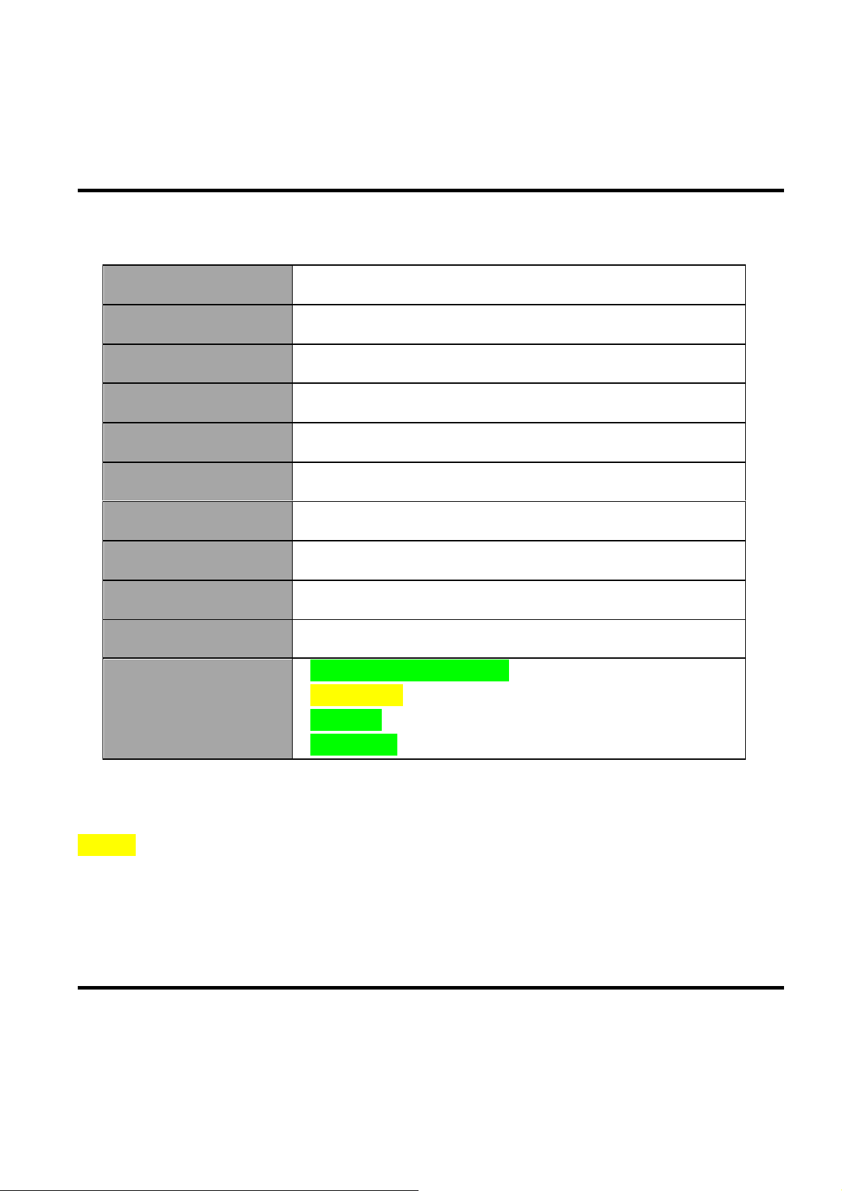
NCC 警語
♦ 根據 NCC 低功率電波輻射性電機管理辦法規定:
第十二條 經型式認證合格之低功率射頻電機,非經許可,公司、商號或使用者均不得擅自變更頻率、加大功率或變更原設計之特性及功能。
第十四條 低功率射頻電機之使用不得影響飛航安全及干擾合法通信;經發現有干擾現象時,應立即停用,並改善至無干擾時方得繼續使用。前
項合法通信,指依電信法規定作業之無線電通信。低功率射頻電機須忍受合法通信或工業、科學及醫療用電波輻射性電機設備之干擾。
-40℃ ~ +85 ℃
-40℃ ~ +85 ℃
3
FCC: H79DFBM-NW726-DT0
CE Compliant
NCC: TBD
TELEC: TBD
Table 3-1. General Specification
Preliminary Data Sheet Sheet 6 of 23 March 8, 2018
Proprietary Information and Specifications are Subject to Change
Page 7
4. Electrical Characteristics
4-1. Absolute Maximum Rating
Symbol Min. Max. Units
VDD_3V3 -0.3 3.9 V
DFBM-NW726-DT0R
V
GPIO
ESD-HBM 2 KV
ESD-CDM 500 V
Table 4-1.Absolute Maximum Rating
-0.3 3.9 V
4-2. Recommended Operating Conditions & Power Consumption
Symbol Parameter
Supply Voltage 1.7 3.3 3.6 V
System On,Standby mode 50 uA
TX Current atPOUT = +0 dBm (LDO) 11.6 mA
TX Current atPOUT = +0 dBm (DCDC) 5.3 mA
VDD_3V3
RX Current (LDO) 12.9 mA
RX Current (DCDC) 5.8 mA
Current inSYSTEM OFF, no RAM retention.
Current inSYSTEM OFF mode 32 kB RAM retention. 1.0 uA
Min. Typ. Max.
0.7
1.2
1.9
Unit
uA
SYSTEM-ON base current with 32 kB RAM enabled. 1.5 uA
Table 4-2. Bluetooth Power Consumption
Preliminary Data Sheet Sheet 7 of 23 March 8, 2018
Proprietary Information and Specifications are Subject to Change
Page 8

DFBM-NW726-DT0R
5. RF Characteristics
5-1. Bluetooth RF characteristics
Condition: VDD_3V3=VIO=3.3V, T=25℃
Item Condition Min. Typ. Max. Unit
RF Characteristics
Output Power -20 0 4 dBm
Initial Frequency Offset -75 75 KHz
Carrier Frequency Offset and Drift CFOD -150 150 KHz
Modulation Index (F1 / F2) 0.8 N/A
Modulation Characteristics
Sensitivity PER < 30.8% -96 dBm
Maximum Input Level PER < 30.8% -10 dBm
Hereby, Delta Electronics, Inc declares that theradio equipment type DFBM-NW726-DT0R is in compliance with
Directive 2014/53/EU. The fulltext of the EU declaration of conformity is available on User Manual
Power and Frequency Ranges
RadioType Description Frequency Maximum Output
Bluetooth Bluetooth5.0-LE 2.402- 2.48 MHz 4 dBm
F1Average 225 275 KHz
F2 Maximum 185 KHz
Table 5-1.Bluetooth RF Characteristics
5-2. Antenna characteristics
There is no antenna on module. Only RF pad is used for antenna. Below table shows antenna list used
for certification testing.
Antenna Designation for
Certification
1. DipoleAntenna, Gain: 2.23dBi
Part No.:RFDPA8780900SMAB801, Supplier: Walsin
Preliminary Data Sheet Sheet 8 of 23 March 8, 2018
Proprietary Information and Specifications are Subject to Change
Page 9

DFBM-NW726-DT0R
2. Chip Antenna, Gain: 2.12dBi
Part No.:RFANT3216120A5T, Supplier: Walsin
3. PCB Antenna, Gain: 2dBi
Part No.:DFAM-NW726-DT0R, Supplier: Delta
6. Pin Description
Pin Definition Function Description
1 GND Gnd Ground
2
3
4 P0.19 Digital I/O Bluetooth general purpose I/O pin
5
6 GND Gnd Ground
7 RF_OUT RF_OUT Bluetooth RFinput/output from IC
8 AOP
9 GND Gnd Ground
10 P0.17 Digital I/O Bluetooth general purpose I/O pin
11
12 GND Gnd Ground
P0.21
nRESET
P0.20
TRACECLK
P0.18
TRACEDATA[0] /
SWO
P0.16
TRACEDATA[1]
Digital I/O
Digital I/O
Digital I/O
AOP_IN
Digital I/O
Bluetooth general purpose I/O pin
Configurable as pin reset
Bluetooth general purpose I/O pin
Trace port clock output
Bluetooth general purpose I/O pin
Single wire output
Trace port output
Bluetooth RF input/output to antenna on package
Bluetooth general purpose I/O pin
Trace port output
13
14 SWDCLK Digital input Serialwire debug clock input for debug and programming
P0.15
Digital I/O
TRACEDATA[2]
Bluetooth general purpose I/O pin
Trace port output
Preliminary Data Sheet Sheet 9 of 23 March 8, 2018
Proprietary Information and Specifications are Subject to Change
Page 10
DFBM-NW726-DT0R
15 SWDIO Digital I/O Serial wire debug I/Ofor debug and programming
16
17 P0.13 Digital I/O Bluetooth general purpose I/O pin
Pin Definition Function Description
18 P0.12 Digital I/O Bluetooth general purpose I/O pin
19 P0.11 Digital I/O Bluetooth general purpose I/O pin
20
21
22 P0.08 Digital I/O Bluetooth general purpose I/O pin
23 GND Gnd Ground
24 P0.07 Digital I/O Bluetooth general purpose I/O pin
25 P0.06 Digital I/O Bluetooth general purpose I/O pin
26
P0.14
TRACEDATA[3]
P0.10
NFC2
P0.09
NFC1
P0.05
AIN3
Digital I/O
Digital I/O
NFC input
D Digital I/O
NFC input
Digital I/O
Analog input
Bluetooth general purpose I/O pin
Trace port output
Bluetooth general purpose I/O pin
NFC antenna connection
Bluetooth general purpose I/O pin
NFC antenna connection
Bluetooth general purpose I/O pin
SAADC/COMP/LPCOMP input
27
P0.04
AIN2
P0.03
28
AIN1
29 VDD Power Power supply input
30 DCC Power DC/DC regulator output
31 DEC4 Power
P0.02
32
AIN0
P0.01
33
XL2
34 P0.00 Digital I/O Bluetooth general purpose I/O pin
Digital I/O
Analog input
Digital I/O
Analog input
Digital I/O
Analog input
Digital I/O
Analog input
Bluetooth general purpose I/O pin
SAADC/COMP/LPCOMP input
Bluetooth general purpose I/O pin
SAADC/COMP/LPCOMP input
1.3 V regulator supply decoupling Input from DC/DC
regulator Output from 1.3 V LDO
Bluetooth general purpose I/O pin
SAADC/COMP/LPCOMP input
Bluetooth general purpose I/O pin
Connection for 32.768 kHz crystal (LFXO)
Preliminary Data Sheet Sheet 10 of 23 March 8, 2018
Proprietary Information and Specifications are Subject to Change
Page 11

DFBM-NW726-DT0R
XL1 Analog input Connection for 32.768 kHz crystal (LFXO)
35 P0.31 Digital I/O Bluetooth general purpose I/O pin
36 P0.30 Digital I/O Bluetooth general purpose I/O pin
Pin Definition Function Description
37 P0.29 Digital I/O Bluetooth general purpose I/O pin
38 P0.28 Digital I/O Bluetooth general purpose I/O pin
39 P0.27 Digital I/O Bluetooth general purpose I/O pin
40 P0.26 Digital I/O Bluetooth general purpose I/O pin
41 P0.25 Digital I/O Bluetooth general purpose I/O pin
42 P0.24 Digital I/O Bluetooth general purpose I/O pin
43 P0.23 Digital I/O Bluetooth general purpose I/O pin
44 P0.22 Digital I/O Bluetooth general purpose I/O pin
45 GND Gnd Ground
46 GND Gnd Ground
47 GND Gnd Ground
48 GND Gnd Ground
Preliminary Data Sheet Sheet 11 of 23 March 8, 2018
Proprietary Information and Specifications are Subject to Change
Page 12

7. Reference Circuit
Test Point
7-1. Use Antenna on Package
DFBM-NW726-DT0R
Optional:
Real Time Clock
Y2
C7
C6
Reserve for
External
Matching Network
C4
NC_0402
R1
0R_0402
C5
NC_0402
P0.21 / nRESET
Test Point
P0.18 / SWO
RF_OUT
AOP_IN
Test Point
P0.20
P0.19
P0.17
P0.16
Module
1
GND
2
P0.21 / nRESET
3
P0.20
4
P0.19
5
P0.18
6
GND
7
RF_OUT
8
AOP
9
GND
10
P0.17
11
P0.16
12
GND
45
GND
GND46GND47GND
P0.23
P0.22
44
P0.25
P0.24
P0.27
P0.26
DFBM-NW726-DT0R
RF OUT
AOP IN
Debug
P0.1416P0.13
P0.1513SWDCLK14SWDIO
48
15
P0.15
P0.1218P0.11
17
P0.13
P0.14
P0.12
SWDIOSWDCLK
19
P0.28
P0.11
P0.29
P0.30
36
P0.30
P0.2937P0.2838P0.2739P0.2640P0.2541P0.2442P0.2343P0.22
P0.10 / NFC220P0.09 / NFC121P0.08
P0.09
P0.10
P0.31
35
P0.31
P0.00 / XL1
P0.01 / XL2
P0.02 / AIN0
POWER
P0.03 / AIN1
P0.04 / AIN2
P0.05 / AIN3
22
P0.08
12pF
DEC4
DCC
VDD
P0.06
P0.07
GND
RTC
34
33
32
31
30
29
28
27
26
25
24
23
12pF
Optional:
DCDC Mode
C3
NC
P0.02
P0.03
P0.04
P0.05
P0.06
P0.07
L3
15nH
L2
10UH
C1
2.2UF
VDD
Figure 7-1. Reference Design Circuit for DFBM-NW726-DT0R (AOP)
Preliminary Data Sheet Sheet 12 of 23 March 8, 2018
Proprietary Information and Specifications are Subject to Change
Page 13

DFBM-NW726-DT0R
Test Point
7-2. Use RF connector or External Antenna
Optional:
Real Time Clock
Y3
C7
C6
Connect to
RF connector or
Antenna
RF_OUT
P0.21 / nRESET
Test Point
P0.18 / SWO
Test Point
P0.20
P0.19
RF_OUT
AOP_IN
P0.17
P0.16
Module
1
GND
2
P0.21 / nRESET
3
P0.20
4
P0.19
5
P0.18
6
GND
7
RF_OUT
8
AOP
9
GND
10
P0.17
11
P0.16
12
GND
45
GND
GND46GND47GND
P0.23
P0.24
P0.22
44
P0.25
P0.26
P0.27
DFBM-NW726-DT0R
RF OUT
AOP IN
Debug
P0.1513SWDCLK14SWDIO
48
P0.15
SWDCLK
P0.1416P0.13
17
15
P0.14
P0.13
P0.12
SWDIO
P0.1218P0.11
19
P0.28
P0.11
P0.29
P0.30
36
P0.30
P0.2937P0.2838P0.2739P0.2640P0.2541P0.2442P0.2343P0.22
P0.10 / NFC220P0.09 / NFC121P0.08
P0.10
P0.09
P0.31
35
P0.31
P0.00 / XL1
P0.01 / XL2
P0.02 / AIN0
POWER
P0.03 / AIN1
P0.04 / AIN2
P0.05 / AIN3
22
P0.08
12pF
DEC4
DCC
VDD
P0.06
P0.07
GND
RTC
34
33
32
31
30
29
28
27
26
25
24
23
12pF
Optional:
DCDC Mode
C3
NC
P0.02
P0.03
P0.04
P0.05
P0.06
P0.07
L3
15nH
L2
10UH
C1
2.2UF
VDD
Figure 7-2. Reference Design Circuit for DFBM-NW726-DT0R (External Antenna)
Preliminary Data Sheet Sheet 13 of 23 March 8, 2018
Proprietary Information and Specifications are Subject to Change
Page 14

8. Module Dimensions (mm)
DFBM-NW726-DT0R
Top View
Side View
Figure 8-1. DFBM-NW726-DT0R Module Dimension
Preliminary Data Sheet Sheet 14 of 23 March 8, 2018
Proprietary Information and Specifications are Subject to Change
Page 15

DFBM-NW726-DT0R
Top View
Figure 8-2. DFBM-NW726-DT0R Module Pin Number
Preliminary Data Sheet Sheet 15 of 23 March 8, 2018
Proprietary Information and Specifications are Subject to Change
Page 16

DFBM-NW726-DT0R
9. Recommend Soldering Conditions
Figure 9-1. Reflow temperature Profile
No. Item Temperature (°C) Time (sec)
1 Pre-heat T
2 Soldering TL: >= 217°C tL: 60~150
3 Peak-Temp. Tp: 260 °C tp: 30
Table 9-1. Reflow temperature Profile Parameters
Preliminary Data Sheet Sheet 16 of 23 March 8, 2018
Proprietary Information and Specifications are Subject to Change
: 150 °C ~ T
smin
: 200°C ts: 60 ~ 120
smax
Page 17

10. Layout Guide (mm)
10-1. Use Antenna on Package
10mm
DFBM-NW726-DT0R
Matching
8.1mm
Circuit
1.8mm
4.8mm
6.7mm
Top Layer Bottom Layer
Figure 10-1. Layout Guide
10-2. Use RF connector or External Antenna
Trace of RF_OUT should be controlled as 50 Ohm stripline or mirco-stripline design.
3.8mm
2.5mm
5.5mm
6.7mm
3mm
4.8mm
Preliminary Data Sheet Sheet 17 of 23 March 8, 2018
Proprietary Information and Specifications are Subject to Change
Page 18

DFBM-NW726-DT0R
11. Recommended StencilAperture
Top View
Figure 11-1.Recommended Stencil Aperture
Preliminary Data Sheet Sheet 18 of 23 March 8, 2018
Proprietary Information and Specifications are Subject to Change
Page 19

DFBM-NW726-DT0R
Top View
Figure 11-2.Recommended Stencil Aperture
Preliminary Data Sheet Sheet 19 of 23 March 8, 2018
Proprietary Information and Specifications are Subject to Change
Page 20

12. Packages
12-1. Tape and Reel Specification
Figure 12-1. Information of Tape specification
DFBM-NW726-DT0R
Figure 12-2. Information of Reel specification
Preliminary Data Sheet Sheet 20 of 23 March 8, 2018
Proprietary Information and Specifications are Subject to Change
Page 21

12-2. Storage Specification
DFBM-NW726-DT0R
Figure 12-4. MSL3 definition
Preliminary Data Sheet Sheet 21 of 23 March 8, 2018
Proprietary Information and Specifications are Subject to Change
Page 22

DFBM-NW726-DT0R
13. Required End Product Labeling
Any device incorporating this module must include an external, visible, permanent marking or label
which states: “Contains FCC ID: H79DFBM-NW726-DT0.”
14. Manual Information to the End User
The OEM integrator has to be aware not to provide information to the end user regarding how to
install or remove this RF module in the user’s manual of the end product which integrates this
module. The end user manual shall include all required regulatory information/warming as shownin
this manual.
15. Federal Communications Commission (FCC)
Statement
15.21
You are cautioned that changes or modifications not expressly approved by the part responsible for
compliance could void the user’s authority to operate the equipment.
15.105(b)
This equipment has been tested and found to comply with the limitsfor a Class B digital device,
pursuant to part 15 of the FCC rules. These limits are designed to provide reasonable protection
against harmfulinterference in a residential installation.
This equipment generates uses and can radiate radio frequency energy and, if not installed and
usedin accordance with the instructions, may cause harmful interference to radio communications.
However, there is no guarantee that interference will not occur in a particular installation. If this
equipment does cause harmful interference to radio or television reception, which can be
determined by turning the equipment off and on, the user is encouraged to try to correct the
interference by one or more of the following measures:
Preliminary Data Sheet Sheet 22 of 23 March 8, 2018
Proprietary Information and Specifications are Subject to Change
Page 23

DFBM-NW726-DT0R
-Reorient or relocate the receiving antenna.
-Increase the separation between the equipment and receiver.
-Connect the equipment into an outlet on a circuit different from that to which the receiver is
connected.
-Consult the dealer or an experienced radio/TV technician for help.
This device complies with part 15 of the FCC Rules. Operation is subject to the following two
conditions:
1) this device may not cause interference and
2) this device must accept any interference, including interference that may cause undesired
operation of the device.
RF Radiation Exposure Statement:
ThisTransmitter must not be co-located or operating in conjunction with any other antenna or
transmitter.
This equipment complies with FCC RF radiation exposure limits set forth for an uncontrolled
environment. This equipment should be installed and operated with a minimum distance of 20
centimeters between the radiator and your body.
Preliminary Data Sheet Sheet 23 of 23 March 8, 2018
Proprietary Information and Specifications are Subject to Change
 Loading...