

Page 1
1
Datasheet
DFBM-NQ62X-DT0R
DFBM-NQ62X-DT0R
A Bluetooth Low Energy System On Chip
Module.
Preliminary Data Sheet Sheet 1 of 18 Aug. 16, 2016
Proprietary Information and Specifications are Subject to Change
Page 2

DFBM-NQ62X-DT0R
Contents
1. Features ........................................................................................................................................... 3
1-1. General ......................................................................................................................................... 3
1-2. Bluetooth...................................................................................................................................... 3
2. Model No. Definition ...................................................................................................................... 4
3. Block Diagram ................................................................................................................................ 6
4. General Specification ...................................................................................................................... 7
5. Electrical Characteristics ................................................................................................................. 8
5-1. Absolute Maximum Rating .......................................................................................................... 8
5-2. Recommended Operating Conditions .......................................................................................... 8
6. RF Characteristics ........................................................................................................................... 9
6-1. Bluetooth RF characteristics ........................................................................................................ 9
6-2. Antenna Performance ................................................................................................................... 9
7. Pin Description .............................................................................................................................. 10
8. Reference Circuit .......................................................................................................................... 12
8-1. Standard Mode ........................................................................................................................... 12
9. Module Dimensions ...................................................................................................................... 13
10. Recommend Soldering Conditions ............................................................................................... 14
11. Layout Guide................................................................................................................................. 15
12. Recommended Land Pattern ......................................................................................................... 16
13. Required End Product Labeling .................................................................................................... 17
14. Manual Information to the End User ............................................................................................ 17
15. Federal Communications Commission (FCC) Statement ............................................................. 17
Preliminary Data Sheet Sheet 2 of 18 Aug. 16, 2016
Proprietary Information and Specifications are Subject to Change
Page 3

T
DFBM-NQ62X-DT0R
DFBM-NQ62X-DT0R
BLE SoC Module
his document describes the DFBM-NQ62X-DT0R wireless BLE SoC module hardware specification.
The modules provide cost effective, low power, and flexible platform to add BLE for embedded devices
for a variety of applications, such as wireless sensors and thermostats. It uses BLE SoC, which integrating
the 2.4GHz transceiver, a 32 bit ARM® Cortex M4F CPU, flash memory, and analog and digital peripherals.
1. Features
1-1. General
BLE chip with a single chip antenna or an external RF connector
Integrate a 32 bit ARM® Cortex M4F CPU,512KB flash memory and 64KB RAM
Extra 512KB flash memory for user data storage (Optional)
32.768KHz Real Time Clock (Optional)
12-bit 200kspc ADC - 8 configurable channels with programmable gain
30 General Purpose I/O Pins
Two-wire Master (I2C compatible) support 100K bps and 400K bps
UART baud rate up to 921600 bps
SPI bit rate up to 4M bps
Quadrature Decoder (QDEC)
LGA 36 pin package
Dimension 19.0mm(L) x 11.0mm(W) x 1.8 mm(H)
RoHS compliant
1-2. Bluetooth
Bluetooth 4.2 specification compliant
AES HW encryption
Preliminary Data Sheet Sheet 3 of 18 Aug. 16, 2016
Proprietary Information and Specifications are Subject to Change
Page 4
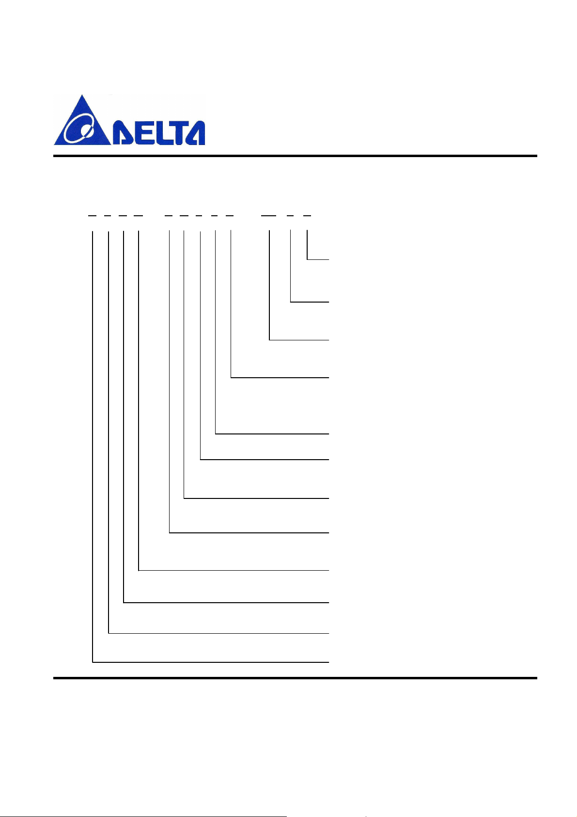
DT = Delta
2. Model No. Definition
D F B M - N Q 6 2 X - DT 0 R
DFBM-NQ62X-DT0R
E = Pb free
R = RoHS
Lead Free
Serial Number
Customer code
Version
N = NG
L = Process with Lead
0 = Consumer Application
0 = Chip Ant+ Flash+ RTC
1 = RF Connector+ Flash+ RTC
2 = Chip Ant+ RTC
3 = RF Connector+ RTC
4 = Chip Ant
5 = RF Connector
Dimension
2 = Class 2
Version
6 = V4.2
Chip Type
Q = QFN
BT Chip
N = Nordic
Product-typ
Property
M = Module
B = Bluetooth
Substrate
F = FR4
Preliminary Data Sheet Sheet 4 of 18 Aug. 16, 2016
Proprietary Information and Specifications are Subject to Change
Company
D = DELTA
Page 5

DFBM-NQ62X-DT0R
Detail Part Number of Module
Part Number
Chip Antenna RF Connector
DFBM-NQ620-DT0R O O O
DFBM-NQ621-DT0R O O O
DFBM-NQ622-DT0R O O
DFBM-NQ623-DT0R O O
DFBM-NQ624-DT0R O
DFBM-NQ625-DT0R O
Antenna Type Storage Flash
(512KB)
Real Time
Clock (RTC)
Preliminary Data Sheet Sheet 5 of 18 Aug. 16, 2016
Proprietary Information and Specifications are Subject to Change
Page 6
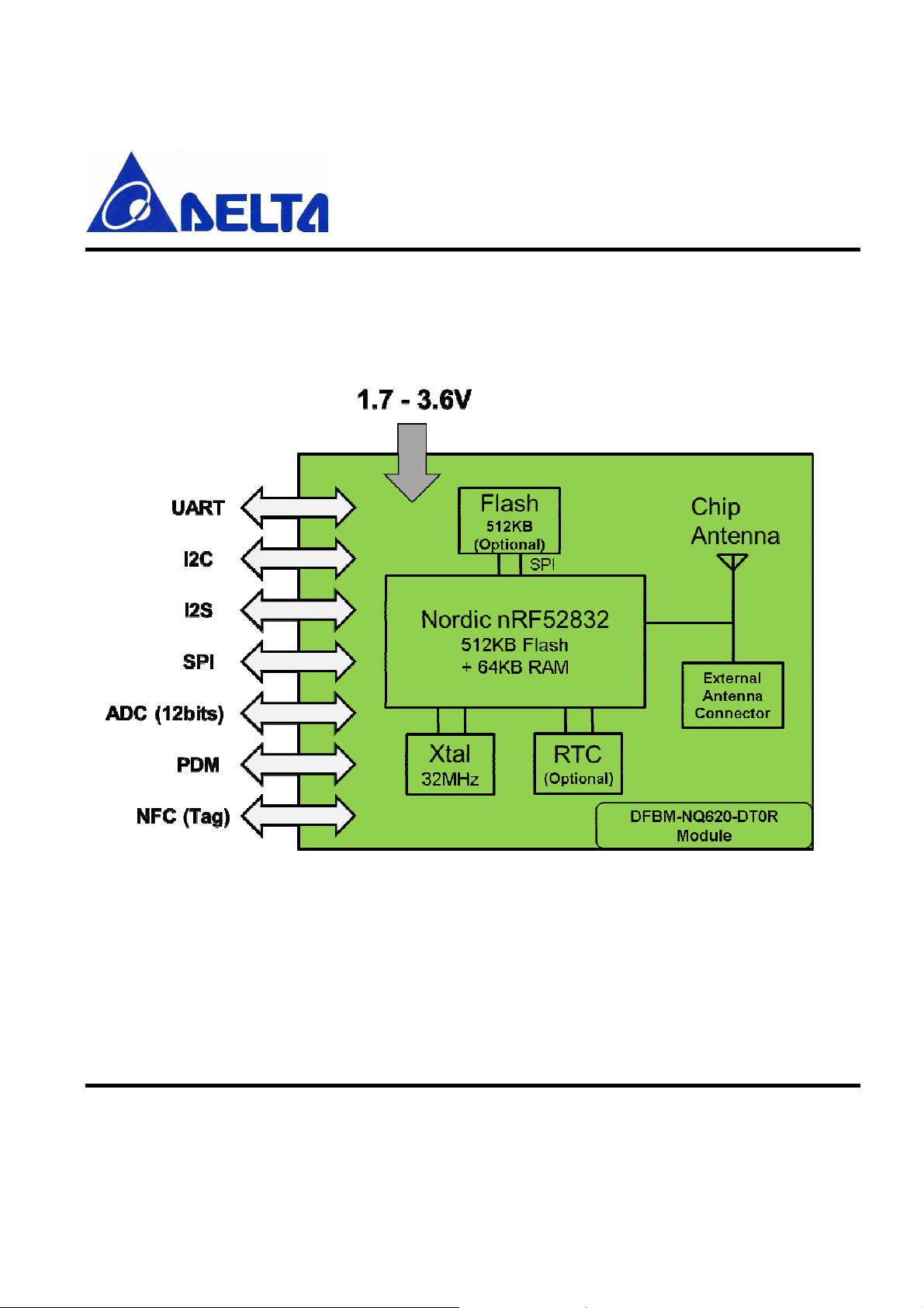
3. Block Diagram
DFBM-NQ62X-DT0R
Figure 3-1. DFBM-NQ620-DT0R Block Diagram
Preliminary Data Sheet Sheet 6 of 18 Aug. 16, 2016
Proprietary Information and Specifications are Subject to Change
Page 7

4. General Specification
Standard
Frequency
Modulation
Data Rate
Operating Temperature
Storage Temperature
Antenna Impedance
Package Size
Bluetooth: V4.2
2.402 ~ 2.48 GHz
GFSK
BLE: 0.25, 1, 2 Mbps
-40~+85 ℃
-40~+125 ℃
50 ohm
19.0 X 11.0 X 1.8 mm
DFBM-NQ62X-DT0R
Host Interface
UART, SPI, I2C
Table 4-1. General Specification
Preliminary Data Sheet Sheet 7 of 18 Aug. 16, 2016
Proprietary Information and Specifications are Subject to Change
Page 8

DFBM-NQ62X-DT0R
5. Electrical Characteristics
5-1. Absolute Maximum Rating
Symbol Min. Max. Units
VDD_3V3 -0.3 3.9 V
V
-0.3 3.9 V
GPIO
ESD-HBM
ESD-CDM 750 V
Table 5-1. Absolute Maximum Rating
5-2. Recommended Operating Conditions
Symbol Parameter
4 KV
Min. Typ. Max.
Unit
1.7 3.3 3.6
3.5
6.5
7.0
1.2
1.0
1.5
V
mA
mA
mA
uA
uA
uA
VDD_3V3
Supply Voltage
System On, Standby mode
TX Current at POUT = +0 dBm
RX Current
Current in SYSTEM OFF, no RAM retention.
Current in SYSTEM OFF mode 32 kB RAM retention.
SYSTEM-ON base current with 32 kB RAM enabled.
Table 5-2. Bluetooth Power Consumption
Preliminary Data Sheet Sheet 8 of 18 Aug. 16, 2016
Proprietary Information and Specifications are Subject to Change
Page 9

DFBM-NQ62X-DT0R
6. RF Characteristics
6-1. Bluetooth RF characteristics
Condition: VDD_3V3=VIO=3.3V, T=25℃
Item Condition Min. Typ. Max. Unit
RF Characteristics
Output Power -20 0 4 dBm
Initial Frequency Offset -75 75 KHz
Carrier Frequency Offset and Drift CFOD -150 150 KHz
Modulation Index (F1 / F2) 0.8 N/A
Modulation Characteristics
Sensitivity PER < 30.8% -96 -70 dBm
Maximum Input Level PER < 30.8% -10 dBm
F1 Average 225 275 KHz
F2 Maximum 185 KHz
Table 6-4. Bluetooth RF Characteristics
6-2. Antenna Performance
Item Specification
Working Frequency Range
Peak Gain (dBi) Chip Antenna: +2dBi
Antenna Type Chip Antenna / External Antenna (Dipole)
VSWR Less than 2.8
Table 6-5. Antenna Characteristics
Preliminary Data Sheet Sheet 9 of 18 Aug. 16, 2016
Proprietary Information and Specifications are Subject to Change
2450 ± 50 MHz
External Antenna: +2dBi
Page 10

DFBM-NQ62X-DT0R
7. Pin Description
Pin
1 GND Gnd Ground
2 P0.25 Digital I/O Bluetooth general purpose I/O pin
3 P0.26 Digital I/O Bluetooth general purpose I/O pin
4 P0.27 Digital I/O Bluetooth general purpose I/O pin
5 P0.28 Digital I/O Bluetooth general purpose I/O pin
6 P0.29 Digital I/O Bluetooth general purpose I/O pin
7 P0.30 Digital I/O Bluetooth general purpose I/O pin
8 P0.31 Digital I/O Bluetooth general purpose I/O pin
9 GND Gnd Ground
10 VDD_3V3 Power VDD power supply input
11 GND Gnd Ground
Definition Function Description
12 GND Gnd Ground
13 GND Gnd Ground
14 P0.02 Digital I/O Bluetooth general purpose I/O pin
15 P0.03 Digital I/O Bluetooth general purpose I/O pin
16 P0.04 Digital I/O Bluetooth general purpose I/O pin
17 P0.09 Digital I/O Bluetooth general purpose I/O pin
18 P0.10 Digital I/O Bluetooth general purpose I/O pin
19 P0.11 Digital I/O Bluetooth general purpose I/O pin
20 P0.12 Digital I/O Bluetooth general purpose I/O pin
21 P0.13 Digital I/O Bluetooth general purpose I/O pin
22 P0.14 Digital I/O Bluetooth general purpose I/O pin
23 P0.15 Digital I/O Bluetooth general purpose I/O pin
24 GND Gnd Ground
Preliminary Data Sheet Sheet 10 of 18 Aug. 16, 2016
Proprietary Information and Specifications are Subject to Change
Page 11

25 P0.16 Digital I/O Bluetooth general purpose I/O pin
26 P0.17 Digital I/O Bluetooth general purpose I/O pin
27 P0.18 Digital I/O Bluetooth general purpose I/O pin
28 P0.19 Digital I/O Bluetooth general purpose I/O pin
29 P0.20 Digital I/O Bluetooth general purpose I/O pin
30 P0.21 Digital I/O Bluetooth general purpose I/O pin
31 SWDCLK Digital input Hardware debug and flash programming I/O
System reset (active low). Also hardware debug and flash
32 SWDIO Digital I/O
programming I/O
33 P0.22 Digital I/O Bluetooth general purpose I/O pin
34 P0.23 Digital I/O Bluetooth general purpose I/O pin
35 P0.24 Digital I/O Bluetooth general purpose I/O pin
36 GND Gnd Ground
Table 7-1. Pin Description
DFBM-NQ62X-DT0R
Preliminary Data Sheet Sheet 11 of 18 Aug. 16, 2016
Proprietary Information and Specifications are Subject to Change
Page 12

8. Reference Circuit
8-1. Standard Mode
DFBM-NQ62X-DT0R
Figure 8-1. DFBM-NQ62X-DT0R Reference Circuit
Preliminary Data Sheet Sheet 12 of 18 Aug. 16, 2016
Proprietary Information and Specifications are Subject to Change
Page 13

9. Module Dimensions
DFBM-NQ62X-DT0R
Figure 9-1. DFBM-NQ62X-DT0R Module Dimension
Preliminary Data Sheet Sheet 13 of 18 Aug. 16, 2016
Proprietary Information and Specifications are Subject to Change
Page 14

smin
smax
DFBM-NQ62X-DT0R
10. Recommend Soldering Conditions
Figure 10-1. Reflow temperature Profile
No.
1 Pre-heat T
2 Soldering TL: >= 217°C tL: 60~150
3 Peak-Temp. Tp: 260 °C tp: 30
Preliminary Data Sheet Sheet 14 of 18 Aug. 16, 2016
Proprietary Information and Specifications are Subject to Change
Item Temperature (°C) Time (sec)
: 150 °C ~ T
Table 10-2. Reflow temperature Profile Parameters
: 200°C ts: 60 ~ 120
Page 15

DFBM-NQ62X-DT0R
11. Layout Guide
1. All traces can fan out directly.
2. To have basic radiation performance. Recommend to keep antenna area (below red block, 11.0 mm
x 4.2 mm) clean and 5 mm extended.
3. To have better radiation performance, more clearance area is needed. Recommend to keep any
metal out from antenna clearance and 20 mm extended.
4. Thickness of system board will make antenna resonant frequency shift. Recommend thickness of
system board is 1.0mm which resonant frequency is 2.5GHz. Resonant frequency will be close to
2.45GHz after assembly in plastic housing.
Extend 20mm
Extend 20mm
Extend 20mm
Antenna Clearance Area
Figure 11-1. Layout Guide
Figure 11-2. Thickness of system board
Preliminary Data Sheet Sheet 15 of 18 Aug. 16, 2016
Proprietary Information and Specifications are Subject to Change
Page 16

DFBM-NQ62X-DT0R
12. Recommended Land Pattern
Figure 12-1. Recommended Stencil Aperture
Preliminary Data Sheet Sheet 16 of 18 Aug. 16, 2016
Proprietary Information and Specifications are Subject to Change
Page 17

DFBM-NQ62X-DT0R
13. Required End Product Labeling
Any device incorporating this module must include an external, visible, permanent marking or label
which states: “Contains FCC ID: H79DFBM-NQ62X.”
14. Manual Information to the End User
The OEM integrator has to be aware not to provide information to the end user regarding how to
install or remove this RF module in the user’s manual of the end product which integrates this
module. The end user manual shall include all required regulatory information/warming as shown in
this manual.
15. Federal Communications Commission (FCC)
Statement
15.21
You are cautioned that changes or modifications not expressly approved by the part responsible for
compliance could void the user’s authority to operate the equipment.
15.105(b)
This equipment has been tested and found to comply with the limits for a Class B digital device,
pursuant to part 15 of the FCC rules. These limits are designed to provide reasonable protection
against harmful interference in a residential installation.
This equipment generates uses and can radiate radio frequency energy and, if not installed and
used in accordance with the instructions, may cause harmful interference to radio communications.
However, there is no guarantee that interference will not occur in a particular installation. If this
equipment does cause harmful interference to radio or television reception, which can be
determined by turning the equipment off and on, the user is encouraged to try to correct the
interference by one or more of the following measures:
Preliminary Data Sheet Sheet 17 of 18 Aug. 16, 2016
Proprietary Information and Specifications are Subject to Change
Page 18

-Reorient or relocate the receiving antenna.
-Increase the separation between the equipment and receiver.
-Connect the equipment into an outlet on a circuit different from that to which the receiver is
connected.
-Consult the dealer or an experienced radio/TV technician for help.
This device complies with part 15 of the FCC Rules. Operation is subject to the following two
conditions:
1) this device may not cause interference and
2) this device must accept any interference, including interference that may cause undesired
operation of the device.
RF Radiation Exposure Statement:
DFBM-NQ62X-DT0R
This Transmitter must not be co-located or operating in conjunction with any other antenna or
transmitter.
This equipment complies with FCC RF radiation exposure limits set forth for an uncontrolled
environment. This equipment should be installed and operated with a minimum distance of 20
centimeters between the radiator and your body.
Preliminary Data Sheet Sheet 18 of 18 Aug. 16, 2016
Proprietary Information and Specifications are Subject to Change
 Loading...