

Page 1
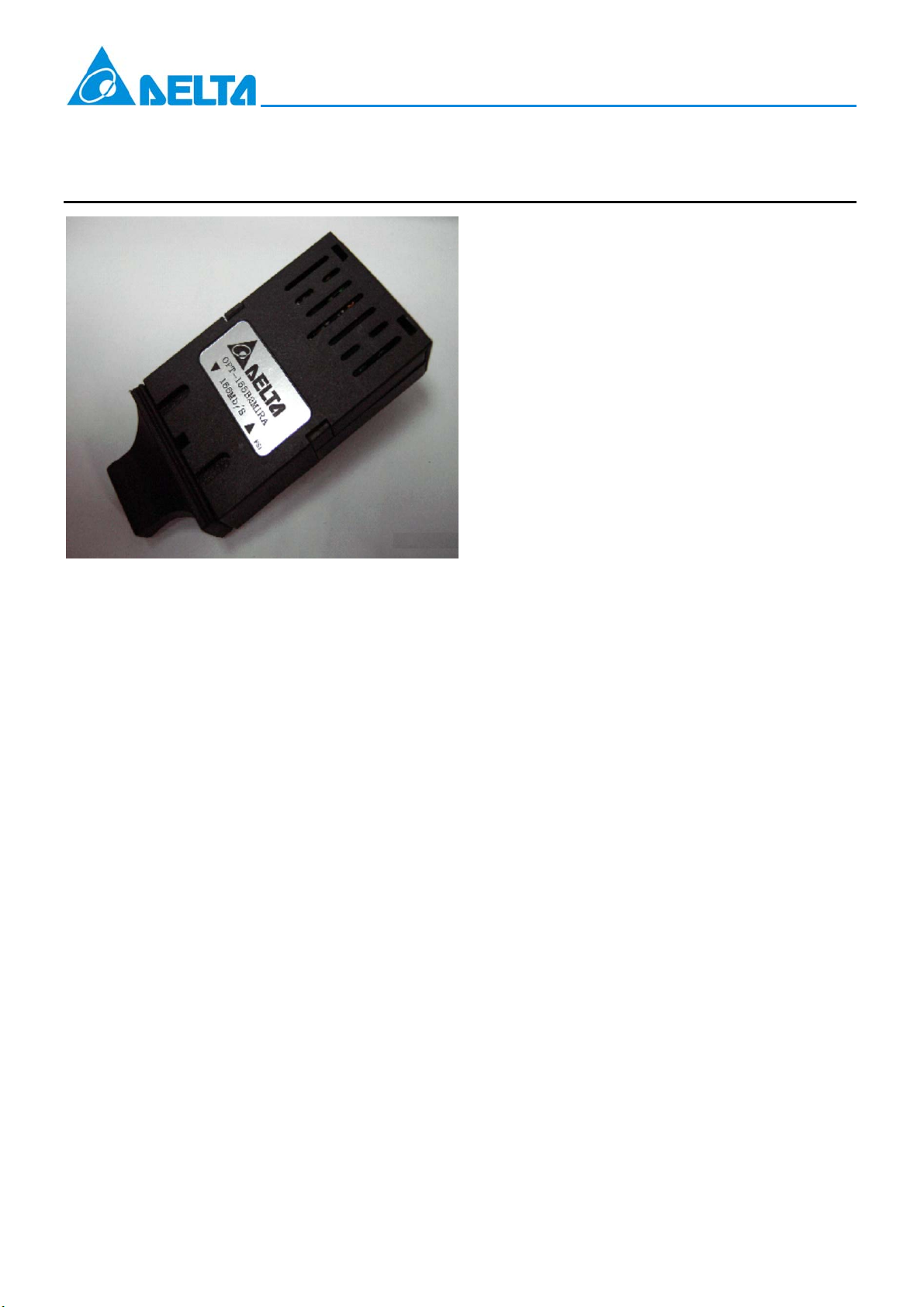
OPT-155Bxxxxxx
155Mbps 1x9 SC Duplex Optical Transceiver Module for
Fast Ethernet, ATM, SONET/OC-3, SDH/STM-1
Features:
Full Compliance with the Optical Performance
Requirements of the ATM 100Mbps and 100
Base-FX Version of IEEE 802.3u.
Industry Standard 1x9 Footprint and Duplex
SC Connector Interface.
Single 5V(OPT-155B1xxxxx)or 3.3V
(OPT-155B2xxxxx)Power Supply.
PECL Differential Inputs and Outputs.
PECL Receiver Signal Detect Indicator.
RoHS Compliance.
Wave Solder and Aqueous Wash Process
Compatible.
Description:
The OPT-155Bxxxxxx series are 1x9 optical
transceiver modules designed expressly for
high-speed communication applications that require
rates of up to 155Mbps. They are all compliant with
the SONET/SDH standards.
The OPT-155Bxxxxxx transceivers are supplied in
industry standard 1x9 SIP package style with duplex
SC connector.
The OPT-155Bxxxxxx also includes a Signal-Detect
circuit that provides PECL logic output state.
The OPT-155Bxxxxxx transceivers can meet Class-1
eye safety products and effective distance depending
on ITU-T G.957 standard or power penalty.
The transmitter sections utilize 1310nm Edge Emitting
InGaAsP Laser Diode. This Laser Diode is packaged
in the optical subassembly portion of the transmitter
section. A custom silicon IC that converts differential
PECL logical signals into an analog LD driving current
drives it.
The receiver sections utilize InGaAs PIN photodiodes
coupled into a custom silicon trans-impedance
preamplifier IC. These are packaged in the optical
subassembly portion of receiver.
These PIN / Preamplifier combinations are coupled
into a custom quantizer IC which provides the final
pulse shaping for the logic output and the Signal
Detect function. The data output is differential. The
signal detect output is single-ended.
Application:
Single-mode Fiber Backbone Links.
Fast Ethernet and ATM Compatible.
Single-mode Fiber Media Converter.
DELTA ELECTRONICS, INC.
http://www.deltaww.com
1
Jan., 2008
Rev.:0H
Page 2
OPT-155Bxxxxxx
Absolute Maximum Ratings
Parameter
Storage Temperature Ts -40 85 ºC
Lead Soldering Temperature T
Lead Soldering Time t
Supply Volt age VCC 0 6 V
Symbol Min. Typ. Max. Unit Note
260 ºC
SOLD
10 Sec.
SOLD
Recommended Operating Conditions
Parameter Symbol Min. Typ. Max. Unit Note
Data Rate 100 155.52 200 Mbps
Ambient Operating Temperature TA 0 70 ºC 1
Supply Volt age
OPT-155B1xxxxx
OPT-155B2xxxxx
V
CC
4.75
3.15
5
3.3
5.25
3.45
V
Note: See “Order Information” for detail
Electrical Characteristics
Parameter Symbol Min. Typ. Max. Unit Note
Transmitter
Transmitter Data Input Voltage-Low VIL-VCC -1.81 -1.48 V
Transmitter Data Input Voltage-High VIH-VCC -1.16 -0.88 V
Receiver
Data Output Voltage-Low VOL-VCC -1.95 -1.62 V
Data Output Voltage-High VOH-VCC -1.045 -0.74 V
SD Output Voltage-Low V
SD Output Voltage-High V
-VCC -1.95 -1.62 V
SDL
-VCC -1.045 -0.74 V
SDH
Optical Characteristics
(Data Rate = 155.52Mbps, PRBS=223-1, NRZ, 9/125um SMF)
Parameter Symbol Min. Typ. Max. Unit Note
Transmitter
Supply Current Icc
165
-20 -15 OPT-155BxHxxxx
Mean Launch Power PO
-15 -8
-8 -5 OPT-155BxLxxxx
-5 0
8.2 OPT-155BxHxxxx
Optical Extinction Ratio E.R.
8.2 OPT-155BxJxxxx
8.2 OPT-155BxLxxxx
10
Center Wavelength
λ
C
1270 1310 1360 nm
7.7 OPT-155BxHxxxx
Spectral Width (RMS)
σ
7.7 OPT-155BxJxxxx
7.7 OPT-155BxLxxxx
3
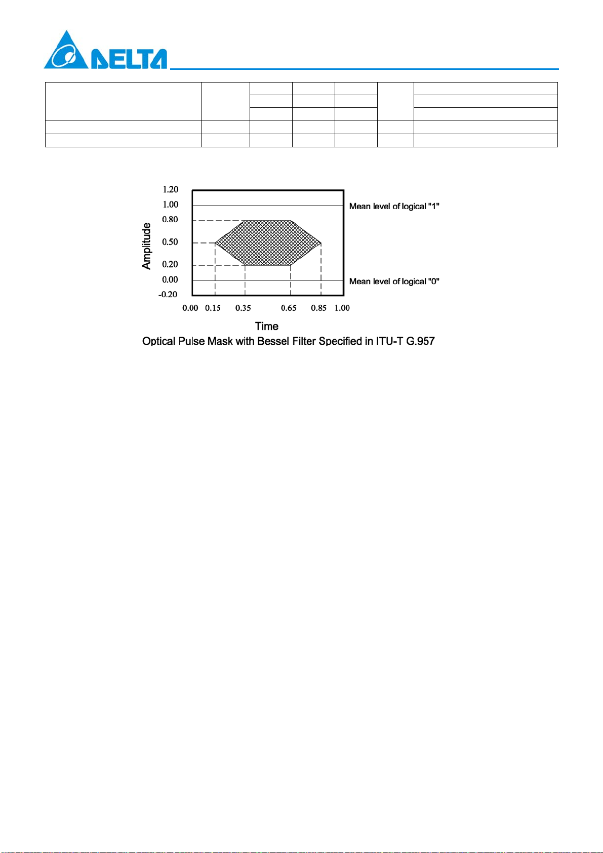
Output Eye Diagram Compliant with ITU-T recommendation G.957
Receiver
Supply Current Icc
145
-31 OPT-155BxHxxxx
Sensitivity PIN
-31 OPT-155BxJxxxx
-31 OPT-155BxLxxxx
-34
Overload P
-8 dBm
SAT
Signal Detect-Asserted PA -31 dBm OPT-155BxHxxxx
DELTA ELECTRONICS, INC.
http://www.deltaww.com
2
mA
OPT-155BxJxxxx
dBm
OPT-155BxMxxxx
dB
OPT-155BxMxxxx
nm
OPT-155BxMxxxx
mA
dBm
OPT-155BxMxxxx
Jan., 2008
Rev.:0H
Page 3
Signal Detect-DeAsserted PD -45 dBm
Signal Detect-Hysteresis PA-PD 0.5 dB
Notes: The sensitivity is provided at a BER of 1×10
PRBS and E.R.=9dB.
-31 OPT-155BxJxxxx
-31 OPT-155BxLxxxx
-34 OPT-155BxMxxxx
-10
or better with an input signal consisting of 155Mbps, 223-1
OPT-155Bxxxxxx
Mask of the eye diagram for the optical transmit signal
DELTA ELECTRONICS, INC.
http://www.deltaww.com
3
Jan., 2008
Rev.:0H
Page 4

Pin Definition
OPT-155Bxxxxxx
PIN Symbol
1 GND Receiver Signal Ground
2 RD (+) Receiver Data Out Non-inverted (LVPECL or PECL)
3 RD (-) Receiver Data Out Inverted (LVPECL or PECL)
4 SD
5 VccR Receiver Power Supply
6 VccT Transmitter Power Supply
7 TD (-) Transmitter Data In Inverted (LVPECL or PECL)
8 TD (+) Transmitter Dat a In Non-inverted (LVPECL or PECL)
9 GND Transmitter Signal Ground
Receiver Signal Detect (LVPECL、PECL)
Functional description
Pin Descriptions
Pin 1 Receiver Signal Ground, GND
Directly connect these pins to the ground plane.
Pin 2 Receiver Data Out Non-inverted (LVPECL), RD (+)
PECL logic family. Output external biased and internal DC coupled.
Pin 3 Receiver Data Out Inverted (LVPECL), RD (-)
PECL logic family. Output external biased and internal DC coupled.
Pin 4 Receiver Signal Detect (LVPECL), SD
PECL logic family. Normal Operation: Logic “1” Output; Fault Condition: Logic”0” Output.
Pin 5 Receiver Power Supply , VccR
Provide +3.3V dc power supply.
Pin 6 Transmitter Power Supply, VccT
Provide +3.3V dc power supply.
Pin 7 Transmitter Data In Inverted (LVPECL), TD (-)
Pin 7 Transmitter Data Input Inverted (LVPECL), TD (-).
Pin 8 Transmitter Data In Non-inverted (LVPECL), TD (+)
Pin 8 Transmitter Data Input Non-inverted (LVPECL), TD (+).
Pin 9 Transmitter Signal Ground, GND
Directly connect these pins to the ground plane.
DELTA ELECTRONICS, INC.
http://www.deltaww.com
4
Jan., 2008
Rev.:0H
Page 5

Recommended Circuit Schematic
OPT-155Bxxxxxx
R1=R3=82 ohm (3.3V),68 ohm(5V)
R2=R4=130 ohm (3.3V),191 ohm (5V)
R5=R6=150 ohm (3.3V),270 ohm (5V)
R7=130 ohm (3.3V PECL),82 ohm(5V),NC (TTL)
R8=82 ohm (3.3V PECL),130 ohm(5V),NC (TTL)
C1=C2=C3=C4=C5=C6=C7=100 nF
C8=C9=10uF
L1=L2=1uH
DELTA ELECTRONICS, INC.
http://www.deltaww.com
5
Jan., 2008
Rev.:0H
Page 6

Package Outline Drawing
OPT-155Bxxxxxx
DELTA ELECTRONICS, INC.
http://www.deltaww.com
6
Jan., 2008
Rev.:0H
Page 7

Regulatory Compliance
OPT-155Bxxxxxx
Feature
Electromagnetic Interference
FCC Class B
Reference
(EMI)
EN 55022 Class B (CISPR 22A)
Radio Frequency
EN 61000-4-3
Electromagnetic Field
IEC 1000-4-3
Electrostatic Discharge to the
EN 61000-4-2
Duplex LC Receptacle
IEC 1000-4-2
IEC 801.2
Electrostatic Discharge to the
Electrical Pins
MIL-STD-883E Method 3015.7
Eye Safety US FDA CDRH AEL Class 1
EN 60950: 2000
EN 60825-1: 1994+A11+A2
EN 60825-2: 2000
Component Recognition Underwriters Laboratories and
Canadian Standards Association Joint
Component Recognition for Information
Technology Equipment Including
Electrical Business Equipment
Performance
(1) Satisfied with electrical
characteristics of product
spec.
(2) No physical damage
CDRH File # 0321539-00
TUV Certificate No. R50032471
UL File # E239394
Order information
OPT- 155BX1X2X3X4X5X6
X
Power Supply Voltage and SD Level
1
X4
1: 5.0V, PECL SD Level
2: 3.3V, PECL SD Level
X
Distance
2
X
J: 15km
M: 40km
X
Data Coupling
3
1: 1x9 SC DC/DC
X
Appendix A.Document Revision
Version No. Date Description
0G 2006-11 Release
0H 2008-01
Update “Recommended Circuit Schematic”,
Correct SD Output Voltage 、Pin Definition、Package Outline、Order
Information
DELTA ELECTRONICS, INC.
http://www.deltaww.com
7
RoHS
Blank: Non-RoHS Compliant
R: RoHS Compliant
Performance
5
Blank: Old Design
A: New Design
6
Temperature
Blank: 0 to +70 degree C
H: -10 to + 85 degree C
T: -40 to + 85 degree C
Jan., 2008
Rev.:0H
 Loading...