

Page 1
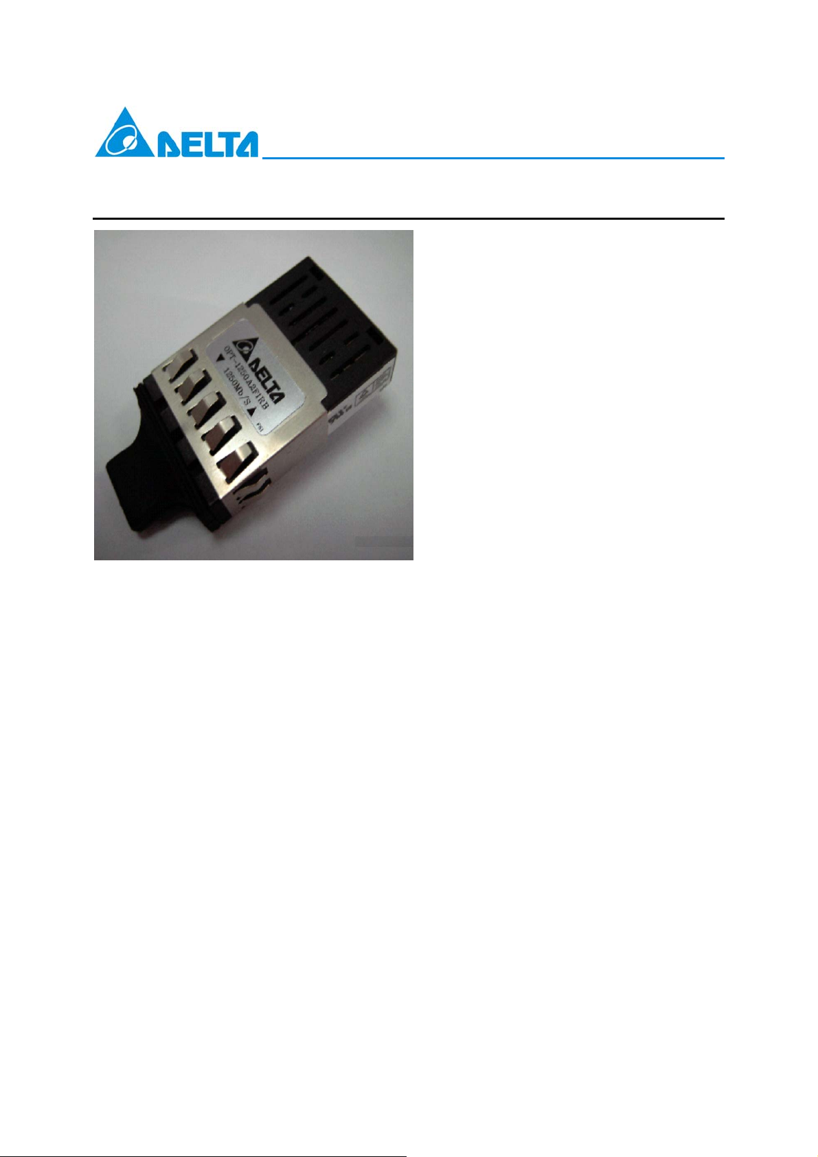
OPT-1250xxxx Series
RoHS Compliant 1X9 SC Duplex Receptacle Transceiver Module for
Gigabit Ethernet
Features
Industry Standard 1 x 9 Footprint and duplex SC
Connector interface
Description
The OPT-1250xxxx series from DELTA is a 1X9
transceiver module designed expressly for
high-speed communication applications that
require rates of up to 1.25Gbit/sec. It is complia nt
with the Gigabit Ethernet standards as well as 1x
Fiber channel standards.
The OPT-1250xxxx transceivers are provided with
the SC receptacle that is compatible with the
industry standard SC connector.
The post-amplifier of the OPT-1250xxxx also
includes a Signal Detect circuit that provides a
PECL or TTL logic-Low output when an unusable
optical signal level is detected. (see order
information)
The OPT-1250xxxx transceiver is a Class 1 eye
safety product. The optical power levels, under
normal operation, are at eye safe level.
Compliant with Specifications for IEEE 802.3z
Gigabit Ethernet
OPT-1250Bxxx compliant with the 1.0625GBd
Fiber Channel 100-SM-LC-L FC-PI Rev.13
OPT-1250Axxx compliant with the 1.0625GBd
Fiber Channel FC-PI 100-M5-SN-I Rev.13
Single +3.3V or 5V Power Supply
PECL or TTL Receiver Signal Detect Indicator
Wave Solderable and Aqueous Washable
Laser Class 1 Product which comply with the
requirements of IEC 60825-1 and IEC 60825-2
RoHS Compliant per Directive 2002/95/EC.
/
Applications
Gigabit Ethernet/Fast Ethernet
Switched backplane applications
Performance
OPT-1250AxFxx:
850nm VCSEL, up to 500m in 50/125μm MMF
850nm VCSEL, up to 220m in 62.5/125μm
MMF
OPT-1250BxQxx:
1310nm FP laser, Data Link up to 10km in
9/125um SMF
1310nm FP laser, up to 550m in 50/125μm
MMF
1310nm FP laser, up to 550m in 62.5/125μm
MMF
DELTA ELECTRONICS, INC.
1 Jan., 2008
Rev. 0H
www.deltaww.com
Page 2
OPT-1250xxxx Series
Absolute Maximum Ratings
Parameter Symbol Min. Typ. Max. Unit Note
Storag e Temperature Ts -40 85 ºC
Lead Soldering Temperature T
Lead Soldering Time t
260 ºC
SOLD
10 sec.
SOLD
Supply Voltage VCC 0 6 V
Recommended Operating Conditions
Parameter Symbol Min. Typ. Max. Unit Note
Ambient Operating Temperature TA 0 70 ºC 1
Supply Voltage
OPT-1250x1xx
OPT-1250x2xx, OPT-1250x4xx
V
CC
4.75
3.135
5.25
V
3.465
Note:
1.See ordering information for detail
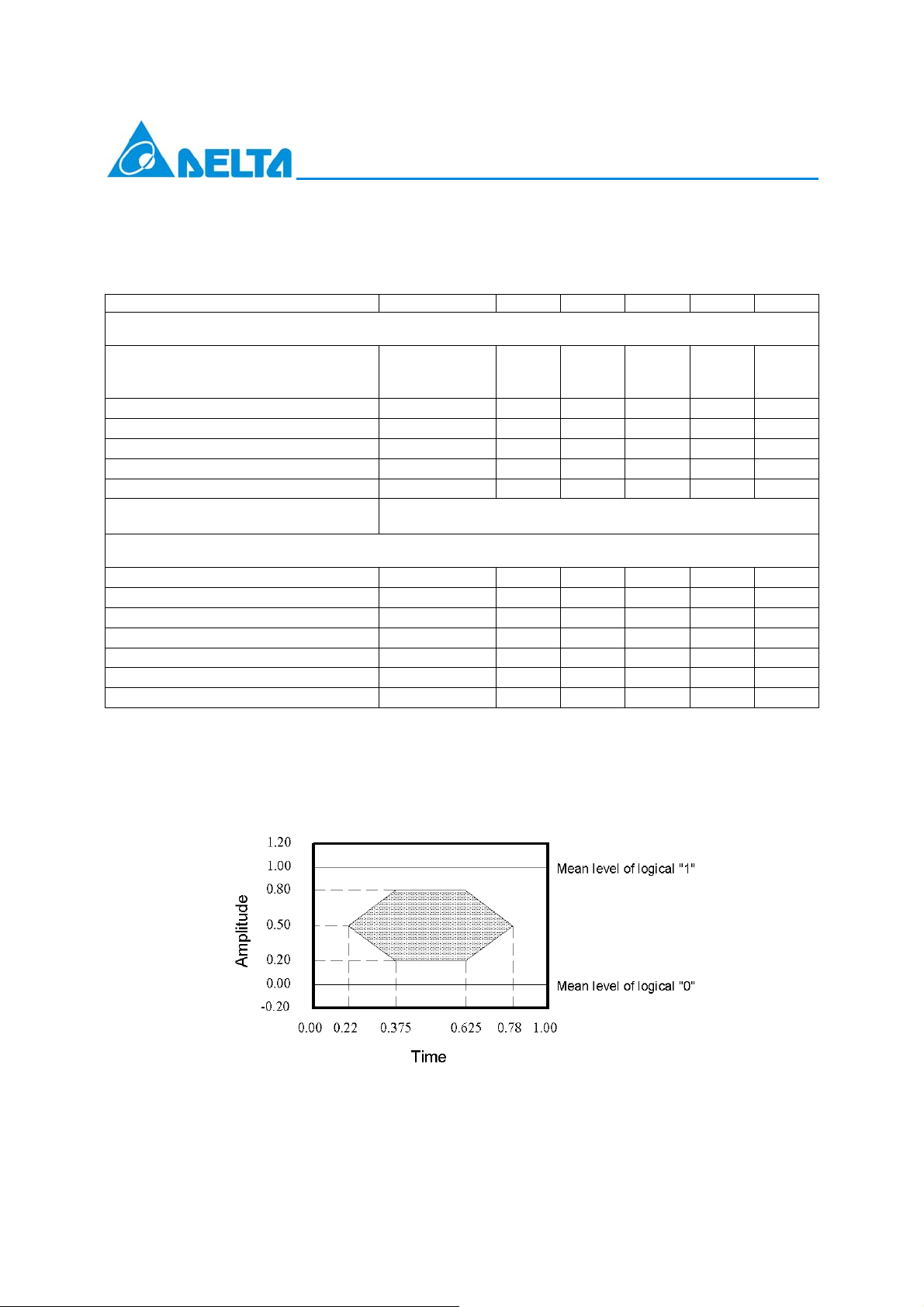
Electrical Characteristics
(At recommended ambient operating temperature, TA and supply voltage, VCC)
Parameter Symbol Min. Typ. Max. Unit Note
Total Supply Current I
Transmitter
Transmitter Data Input Voltage-Low VIL-V
Transmitter Data Input Voltage-High VIH-V
Transmitter Differential Input Voltage VDT 0.3 1.6 V 2
Receiver
Data Output Voltage-Low VOL-V
Data Output Voltage-High VOH-V
Receiver Differential Output Voltage VDR 0.5 0.7 1.2 V 2
Output Data Rise/Fall Time tr/tf 0.4 ns 3
PECL SD Output
LOW level output voltage
HIGH level output voltage
TTL SD Output
LOW level output voltage
HIGH level output voltage
Notes:
1. For OPT-1250A1F1x, OPT-1250A4F1x, OPT-1250B2Q1x and OPT-1250B1Q1x.
310 mA
CCT
-1.810 -1.475 V 1
CC
-1.165 -0.880 V 1
CC
-1.95 -1.62 V 1
CC
-1.045 -0.74 V 1
CC
V
SDL-VCC
V
SDH-VCC
V
SDL
V
SDH
-1.84
-1.1
0
2
-1.60
V 4
-0.9
0.8
V 5
VCC
2. For OPT-1250A2F2x and OPT-1250B4Q2x.
3. These are 20%~80% va lue s
4. For OPT-1250A1F1x, OPT-1250A2F2x, OPT-1250B1Q1x and OPT-1250B2Q1x
5. For OPT-1250A4F1x and OPT-1250B4Q2x
2 Jan., 2008
DELTA ELECTRONICS, INC.
www.deltaww.com
Rev. 0H
Page 3
OPT-1250xxxx Series
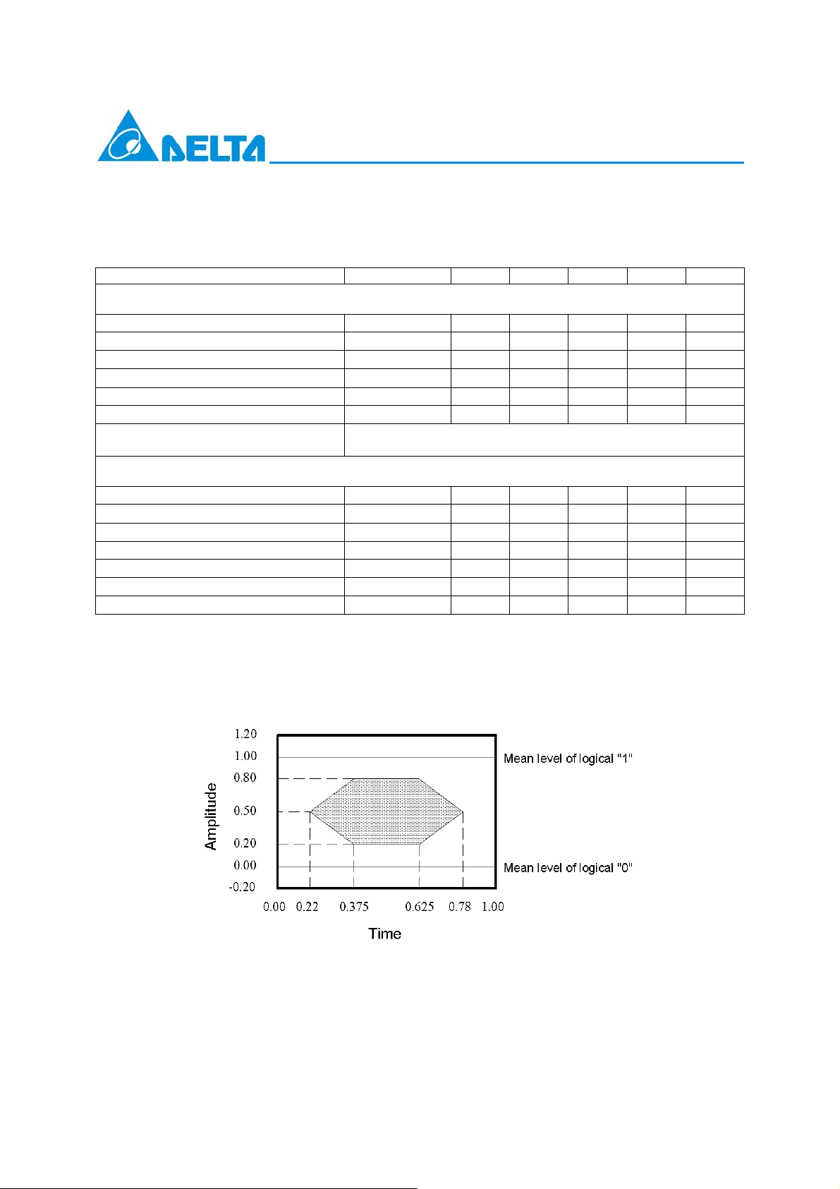
Single Mode Transceiver (OPT-1250B1Q1x, OPT-1250B2Q1x, OPT-1250B4Q2x)
(At recommended ambient operating temperature, TA and supply voltage, VCC; Data Rate=1.25Gb/sec,
7
PRBS=2
Transmitter
Output Optical Power (Avg.)
OPT-1250BxIx
OPT-1250BxQx
Optical Extinction Ratio ER 9 dB
Center Wavelength
Spectral Width (RMS)
Optical Rise/Fall time
Relative Intensity Noise
Output Eye
Receiver
Sensitivity (Avg.) PIN -19 dBm 2
Input Optical Wavelength
Optical Rise/Fall Time
Signal Detect-Asserted (Avg.) PA -19 dBm
Signal Detect-De-asserted (Avg.) PD -35 dBm
Signal Detect-Hysteresis PA-PD 0.5 dB
Receiver Saturation Power P
Notes:
1. These are unfiltered 20%~80% valu es
2. The sensitivity is provided at a BER of 1×10
-1 NRZ, 9/125um SMF)
Parameter Symbol Min. Typ. Max. Unit Note
7
1250Mb/s, 2
-1 PRBS and ER=9dB.
P
O
-12
-9.5
λ
C
σ
0.4 ns 1
t
r/tf
1270 1310 1355 nm
4.5 nm
-3
-3
dBm
RIN -120 dB/Hz
Complies with the IEEE 802.3z/D2 specification, and is class 1
laser eye safety
λ
0.5 ns 1
t
r/tf
-3 dBm
SAT
-10
or better with an input signal consisting of
1310 nm
Mask of the eye diagram for the optical transmit signal
DELTA ELECTRONICS, INC.
3 Jan., 2008
Rev. 0H
www.deltaww.com
Page 4
OPT-1250xxxx Series
Multi-Mode Series Transceiver (OPT-1250A1F1x, OPT-1250A2F2x, OPT-1250A4F1x)
(At recommended ambient operating temperature, TA and supply voltage, VCC; Data Rate=1.25Gb/sec,
7
PRBS=2
Transmitter
Output Optical Power (Avg.) PO -9.5 -4 dBm
Optical Extinction Ratio ER 9 dB
Center Wavelength
Spectral Width (RMS)
Optical Rise/Fall time
Relative Intensity Noise
Output Eye
Receiver
Sensitivity (Avg.) PIN -17 dBm 2
Input Optical Wavelength
Optical Rise/Fall time
Signal Detect-Asserted (Avg.) PA -17 dBm
Signal Detect-De-ass erted (Avg.) PD -30 dBm
Signal Detect-Hysteresis PA-PD 0.5 dB
Receiver saturation power P
Notes:
1. These are 20%~80% va lue s
2. The sensitivity is provided at a BER of 1×10
-1 NRZ, 62.5/125um MMF)
Parameter Symbol Min. Typ. Max. Unit Note
7
1250Mb/s, 2
-1 PRBS and ER=9dB.
λ
C
σ
0.26 ns 1
t
r/tf
830 850 860 nm
0.85 nm
RIN -117 dB/Hz
Complies with the IEEE 802.3z/D2 specification, and is class 1
laser eye safety
λ
0.36 ns 1
t
r/tf
-4 dBm
SAT
-10
or better with an input signal consisting of
850 nm
Mask of the eye diagram for the optical transmit signal
DELTA ELECTRONICS, INC.
4 Jan., 2008
Rev. 0H
www.deltaww.com
Page 5

OPT-1250xxxx Series
Pin Definition
PIN Symbol Functional description
1 GND Receiver Signal Ground
2 RD (+) Receiver Data Out Non-inverted (LVPECL)
3 RD (-) Receiver Data Out Inverted (LVPECL)
4 SD Receiver Signal Detect (LVPECL or TTL)
5 VccR Receiver Power Supply,
6 VccT Transmitter Power Supply
7 TD (-) Transmitter Data In Inverted (LVPECL)
8 TD (+) Transmitter Data In Non-inverted (LVPECL)
9 GND Transmitter Signal Ground
Pin Descriptions
Pin 1 Receiver Signal Ground, GND
Directly connect these pins to the ground plane.
Pin 2 Receiver Data Out Non-inverted (LVPECL), RD (+)
Receiver Data output Non-inverted (LVPECL), RD (+).
Pin 3 Receiver Data Out Inverted (LVPECL), RD (-)
Receiver Data output Inverted (LVPECL), RD (-).
Pin 4 Receiver Signal Detect (LVPECL/TTL), SD
PECL/TTL logic family. Normal Operation: Logic “1” Output
Fault Condition: Logic “0” Output.
Pin 5 Receiver Power Supply, VccR
Provide +3.3/5V dc power supply.
Pin 6 Transmitter Power Supply, VccT
Provide +3.3/5V dc power supply.
Pin 7 Transmitter Data In Inverted (LVPECL), TD (-)
Transmitter Data Input Inverted (LVPECL), TD (-)
Pin 8 Transmitter Data In Non-inverted (LVPECL), TD (+)
Transmitter Data Input Non-inverted (LVPECL), TD (+)
Pin 9 Transmitter Signal Ground, GND
Directly connect these pins to the ground plane.
DELTA ELECTRONICS, INC.
5 Jan., 2008
Rev. 0H
www.deltaww.com
Page 6

OPT-1250xxxx Series
Recommend Circuit Schematic for Internal DC Coupled Transceivers
R1=R3=82 ohm (3.3V),68 ohm(5V)
R2=R4=130 ohm (3.3V),191 ohm (5V)
R5=R6=150 ohm (3.3V),270 ohm (5V)
R7=130 ohm (3.3V PECL),82 ohm(5V),NC (TTL)
R8=82 ohm (3.3V PECL),130 ohm(5V),NC (TTL)
C1=C2=C3=C4=C5=C6=C7=100 nF
C8=C9=10uF
L1=L2=1uH
DELTA ELECTRONICS, INC.
6 Jan., 2008
Rev. 0H
www.deltaww.com
Page 7

OPT-1250xxxx Series
Recommend Circuit Schematic for Internal AC Coupled Transceivers
R1=130 ohm (3.3V PECL),82 ohm(5V),NC (TTL)
R2=82 ohm (3.3V PECL),130 ohm(5V),NC (TTL)
C1=C2=C3= 100 nF
C4=C5=10uF
L1=L2=1uH
DELTA ELECTRONICS, INC.
7 Jan., 2008
Rev. 0H
www.deltaww.com
Page 8

Package Outline Drawing (without shielding)
OPT-1250xxxx Series
Package Outline Drawing (A type shielding)
Class 1 Laser Product
DELTA ELECTRONICS, INC.
8 Jan., 2008
Rev. 0H
www.deltaww.com
Page 9

Package Outline Drawing (B type shielding)
OPT-1250xxxx Series
Package Outline Drawing (C type shielding)
DELTA ELECTRONICS, INC.
9 Jan., 2008
Rev. 0H
www.deltaww.com
Page 10

Regulatory Compliance
Feature Reference Performance
OPT-1250xxxx Series
Electromagnetic Interference
(EMI)
Radio Frequency
Electromagnetic Field
Electrostatic Di scharge to the
Duplex LC Receptacle
Electrostatic Di scharge to the
Electrical Pins
Eye Safety US FDA CDRH AEL Class 1
Component Recognition Underwriters Laboratories and
FCC Class B
EN 55022 Class B (CISPR 22A)
EN 61000-4-3
IEC 1000-4-3
EN 61000-4-2
IEC 1000-4-2
IEC 801.2
MIL-STD-883E Method 3015.7
EN 60950: 2000
EN 60825-1: 1994+A11+A2
EN 60825-2: 2000
Canadian Standards Association Joint
Component Recognition for Information
Technology Equipment Including
Electrical Business Equipment
(1) Satisfied with electrical
characteristics of product
spec.
(2) No physical damage
CDRH File # 0321539-00
TUV Certificate No. R50032471
UL File # E239394
DELTA ELECTRONICS, INC.
10 Jan., 2008
Rev. 0H
www.deltaww.com
Page 11

Ordering Information
OPT- 1250X1X2X3X4X5X6X7
OPT-1250xxxx Series
: Fiber
X
1
A: Multi-mode 850nm
B: Single-mode 1310nm
: Power Supply Voltage and SD Level
X
2
1: 5.0V, PECL SD Level
2: 3.3V, PECL SD Level
: 3.3V, TTL SD Level
4
: RoHS Compliant
X
5
Blank: Non-RoHS Compliant
R: RoHS Compliant
X6: Shielding Type & Revision Code
A: New design
B: B type shielding
C
D: A type shielding
X
:
Distance
3
F: 500m,
Q: 10km,
:
X
4
Data Coupling
50/125μm
9/125μm
MMF
SMF
X
:Temperature
7
Blank: 0 to +70 degree C
H: -10 to + 85 degree C
T: -40 to + 85 degree C
1: 1x9 SC DC/DC
2: 1x9 SC AC/AC
Appendix A.Document Revision
Version No. Date Description
0G 2006-09 Release
0H 2008-01
Correct “Total Supply Current”、 “TTL SD Output”、 “PECL SD
Output”、 Recommend Circuit Schematic、Optical Rise/Fall time、
Spectral Width (RMS)、Pin Definition、Package Outline、Order
Information
: C type shielding
DELTA ELECTRONICS, INC.
11 Jan., 2008
Rev. 0H
www.deltaww.com
 Loading...