

DEI EVIC420-B, EVIC420-A Datasheet
EVIC420
DEIC420 High Frequency Gate Driver IC Evaluation Board
General Description
The EVIC420 evaluation board is a general-purpose circuit
board designed to simplify the evaluation of the DEI
DEIC420 gate drive IC, as well as to provide a building block
for power circuit development. The DEIC420 RF-package
gate driver is factory-installed in the EVIC420. The option A
board enables the user to drive MOSFETs in the DEI DE150 or DE-275 RF package types, and the Option B board
driver DE-375 and DE-475 package type MOSFETs. The
evaluation board design allows both the DEIC420 and the
MOSFET to be attached to a heat sink, and in so doing the
board assembly can be used as a ground referenced, low
side power switch for both single-ended and push-pull
configurations.
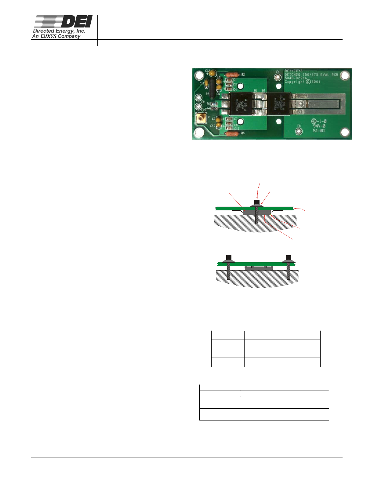
Figure 1 is a photograph of the EVIC420-A Evaluation Board
loaded with a DEIC420 driver and a DE275-102N06A
MOSFET. The low level inputs are shown on the left side of
the board. J1 is a TTL high true input connected to the INA
and INB pins which control the on or off state of the power
switch U2. E9 is the low voltage, (8-30V) power input
connected to VCC-IN of the IC, (see Figure 3 below).
Figure 1 - EVIC420 Evaluation Board
DEI DEIC420 shown in low-power mounting configuration
(see Figure 2). DE275-102N06A MOSFET installed in lowpower configuration for illustration purposes only
#4-40 Socket Heat Screw (Or Equivalent)
3 Inch-Pounds Max. Torque
DE-Series
MOSFET
Belleville Washer
For low-power configurations, the MOSFET and DEIC420
may be mounted on the top of the circuit board, as shown in
Figure 1. However in this configuration, they cannot be
cooled with a heatsink. For high-power applications, the
DEIC420 and MOSFET are mounted on the back side of the
PCB, as shwon in Figure 2. In this configuration, the devices
are placed in compression against a heatsink or cold plate,
facilitating the very high power dissipation capability of the
devices
(1)
. For additional information on device power
dissipation, see the DEIC420 and the appropriate MOSFET
data sheets on the DEI web site at
www.directedenergy.com.
Circuit Operation
The schematic diagram for the evaluation board is shown in
Figure 4. The control gate (J1) is applied to R4 then on the
input lead 2 of the IC U1. This signal input is followed in
time by the output lead 5 of U1, which is connected to the
gate of the MOSFET. Leads 1 and 3 are attached to +VCC
via a de-coupling network comprised of R2 and C3 through
C18. U1 leads 4 and 6 are attached to the circuit ground
plane. This is the preferred arrangement of the bypassing
for the Vcc input power.
The test point E7 is connected to the drain of the MOSFET.
This allows the user to easily attach an oscilloscope probe
and the associated ground to the circuit to verify
performance.
The drain output section is designed to allow the user to
install the load of choice as well as the type of high voltage
bypassing. The Drain pad is labeled E7. The large pad to
the right of E7 is intended for the Vds power supply
connection. Surrounding the drain pad and the Vds pad is a
power ground pad. In the circuit diagram this pad is labeled
E4 and E8.
Printed
Circuit
Heat Sink
Side View
Heat Sink
End View From Drain Side
Figure 2 - EVIC420 Side Views Showing DEIC420 and DESeries Power Devices Installed In High-Power Configura-
(1)
tions
INPUT FUNCTION
J1 (SMB) Control Input - 3V into 1K Ohms
E4, E8, E10 Ground
E9 VCC input - 8V to 25V
Figure 3 - Input Pin-Out Table
(1)
note "DE-Series MOSFET Mounting & Installation Instructions" on
the DEI web site at www.directedenergy.com/apptech.htm.
ORDERING INFORMA T ION
Part Number Installed Device
EVIC420-A Accommodates DEI DE-150 and
DE-275 Series MOSFET Devices
EVIC420-B Accommodates DEI DE-375 and
DE-475 Series MOSFET Devices
For additional device installation instructions, see the technical
Thermal
Compound
Metallic
Substrate
Board
Copyright © Directed Energy, inc. 2002
First Release
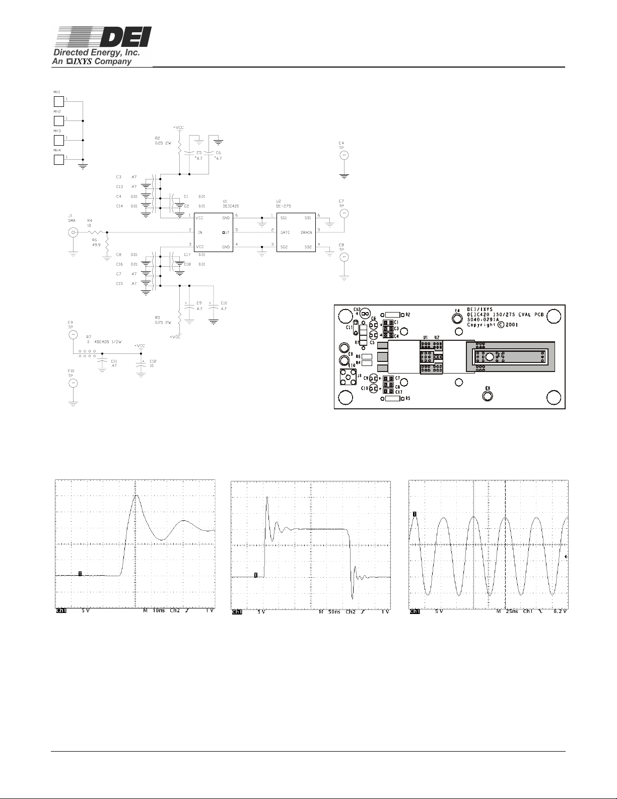
Figure 4 - EVIC420 Schematic Diagram And Circuit Board Layout
EVIC420
NOTES: 1) The schematic shows a DE275 MOSFET, however a DEI DE-150 or DE-275 package type may be installed on the
EVIC420-A, and a DE-375 or DE-475 package type may be installed on the EVIC420-B. The EVIC420 is provided without a
MOSFET, so that the user can install the appropriate MOSFET for their application. DEI MOSFET data sheets are available on
the DEI web site at www.directedenergy.com/Products/specs/deseries.htm.
Figure 5 - EVIC420 3.0ns
Gate Rise Time
CL=1120pF
For additional performance data and electrical waveforms, see the DEIC420 Data Sheet on the DEI web site.
Directed Energy, Inc.
An IXYS Company
2401 Research Blvd. Ste. 108
Ft. Collins, CO 80526
Tel: 970-493-1901; Fax: 970-493-1903
e-mail: deiinfo@directedenergy.com
www.directedenergy.com
Figure 6 - EVIC420 Typical
Gate Waveform
CL=1120pF
Figure 7 - EVIC420 Typical
Output Waveform
F=50MHz Burst, CL=1000pF
Doc #9200-0251 Rev 1
 Loading...