DEI EVDD415, EVDD415 Datasheet

EVDD415
IXDD415 High Frequency Gate Driver IC Evaluation Board
General Description
The EVDD415 evaluation board is a general-purpose circuit
board designed to simplify the evaluation of the IXYS/DEI
IXDD415 gate drive IC, as well as to provide a building block
for power circuit development. The IXDD415SI SO-28
package gate driver is factory-installed in the EVDD415. The
board enables the user to drive MOSFETs in the DEI DE150 or DE-275 RF package types. The evaluation board
design allows these MOSFETS to be attached to a heat
sink, and in so doing the board assembly can be used as a
ground referenced, low side power switch for both singleended and push-pull configurations. Circuitry for the TriState function is included on the evaluation board.
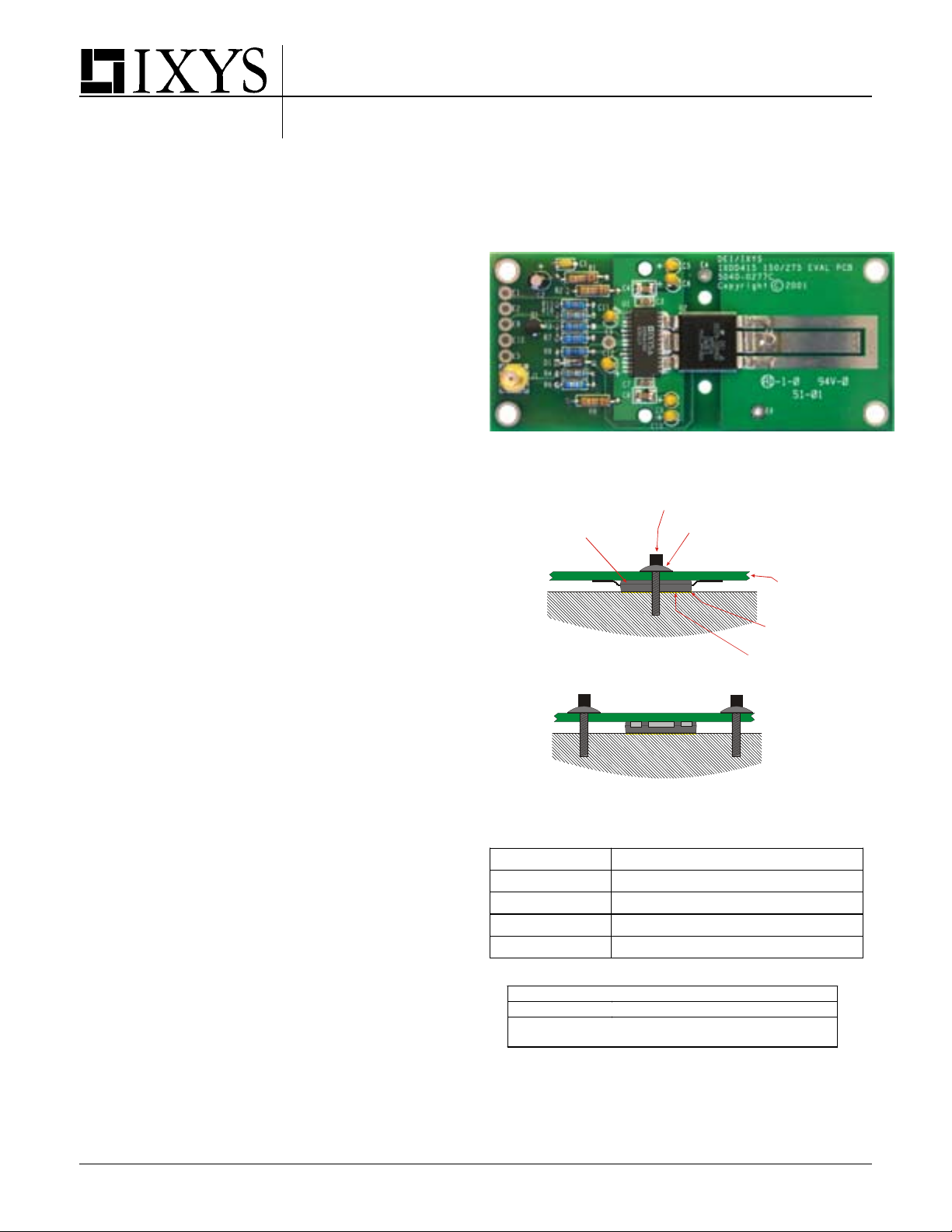
Figure 1 is a photograph of the IXDD415 Evaluation Board
loaded with an IXDD415SI driver and a DE275-102N06A
MOSFET. The low level inputs are shown on the left side of
the board. J1 is a TTL high true input connected to the INA
and INB pins which control the on or off state of the power
switch U2. E9 is a low true input connected to the ENA and
ENB pins, which control the Tri-State output. E1 is the low
voltage, (8-30V) power input connected to VCC-IN of the IC,
(see Figure 3 below). Figure 2 illustrates the MOSFET
mounting of a DE-Series MOSFET. The MOSFET is
mounted on the back side of the PCB.
Circuit Operation
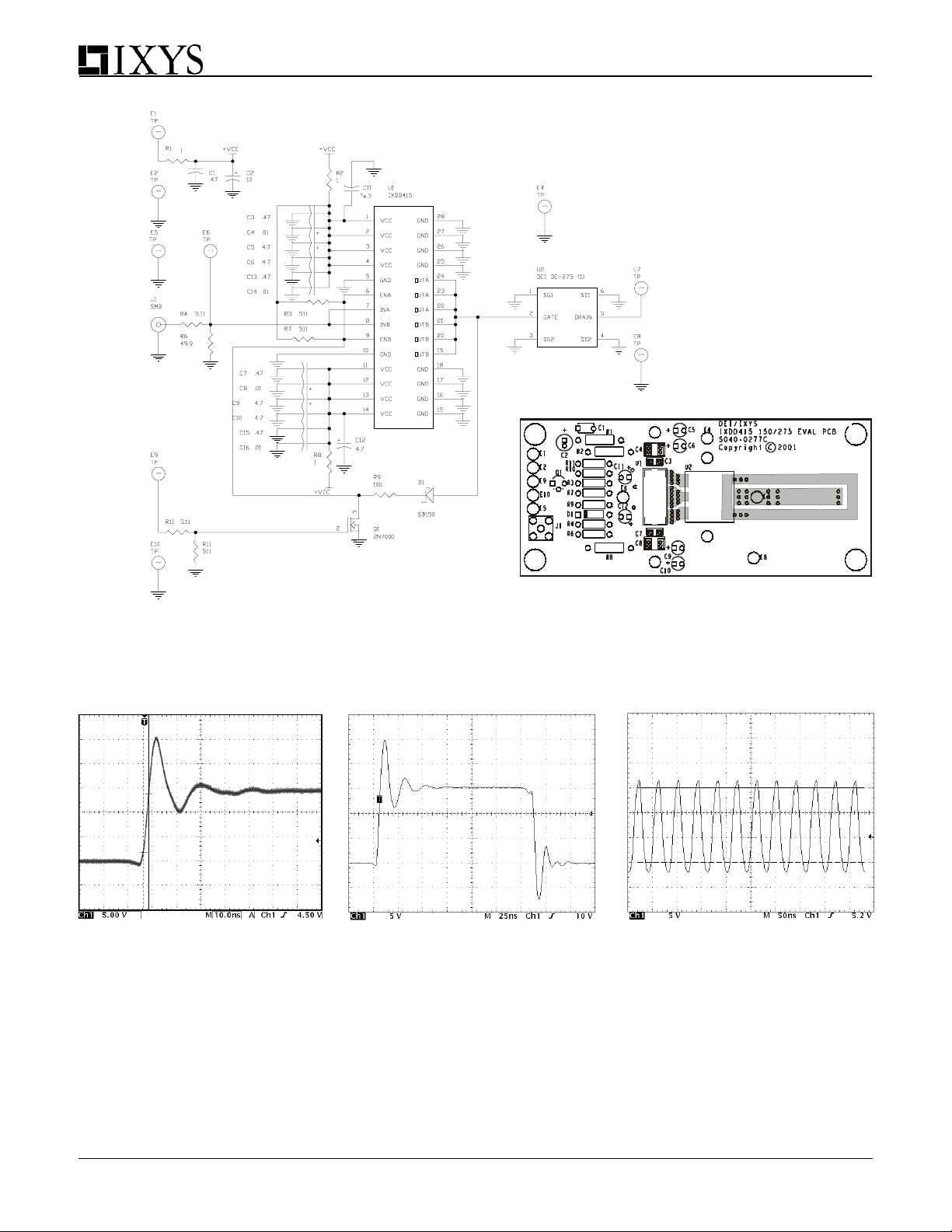
The schematic diagram for the evaluation board is shown in
Figure 4. The control gate is applied to R4 then on the input
pins 7 and 8 of the IC U1. This signal input is followed in
time by the output pins 19 through 24 U1. Pins 1 through 4
and 11 through 14 U1 are attached to +VCC via a decoupling network comprised of R1, C1, C2, C3 through C10
and C13 through C16. Pins 5, 10, 15 through 18 and 25
through 28 U1 are attached to the circuit ground plane. This
is the preferred arrangement of the bypassing for the Vcc
input power. The enable pins 6 and 9 of U1 are attached to
the drain of Q1. This device is used to level translate and
provide an invert function for the Tri-State mode. The drain of
Q1 is also attached to the gate of the MOSFET thru R9 and
D1. In the Tri-State mode the turn off time of the power
MOSFET is determined by the time constant of the input
gate capacitance C
the IXDD415 data sheet for additional information on this
mode of operation.
The U1 output is available at pins 19 through 24 of U1. The
board is designed to parallel the two outputs of the IXDD415
IC, generating up to 20A
pins for each channel should always be paralleled to
reduce circuit inductance, and to provide the current-carrying
capability required for the high output current capability of
the IXDD415.
There are two test points on the board: E6 for Control and
E7 for the Drain. These allow the user to easily attach an
oscilloscope probe and the associated ground to the circuit
to verify performance.
The drain output section is designed to allow the user to
install the load of choice as well as the type of high voltage
and the value of the resistor R9. See
iss
(1)
of output current. The three output
bypassing. The Drain pad is labeled E7. The large pad to
the right of E7 is intended for the Vds power supply
connection. Surrounding the drain pad and the Vds pad is a
power ground pad. In the circuit diagram this pad is labeled
E8.
Figure 1 - EVDD415 Evaluation Board
DEI DE275-102N06A Device Installed In Low-Power Configuration For Illustration Purposes Only
#4-40 Socket Heat Screw (Or Equivalent)
3 Inch-Pounds Max. Torque
DE-Series
MOSFET
Heat Sink
Side View
End View From Drain Side
Figure 2 - EVDD415 Side Views Showing DE-Series Power
Device Installed In A High-Power Configuration
INPUT FUNCTION
J1 (SMB) Control Input - 3V into 1K Ohms
E2, E4, E5, E8, E10 Ground
E9 Enable, LOW = True, HIGH = Tri-State Mode
E1 VCC input - 8V to 25V
Figure 3 - Input Pin-Out Table
ORDERING INFORMATION
Part Number Installed Device
EVDD415 Accommodates DEI DE-150 and
(1)
Each output of the IXDD415 can provide 15A of current, but
when both outputs are driven simultaneously, as with the
EVDD415, the maximum output current should be limited to 20A.
(2)
For additional device installation instructions, see the technical
note "DE-Series MOSFET Mounting & Installation Instructions" on
the DEI web site at www.directedenergy.com/apptech.htm.
DE-275 Series MOSFET Devices
Heat Sink
Belleville Washer
Thermal
Compound
Metallic
Substrate
Printed
Circuit
Board
(2)
Copyright © IXYS CORPORATION 2001
First Release

Figure 4 - EVDD415 Schematic Diagram And Circuit Board Layout
EVDD415
NOTES: 1) The schematic shows a DE275 MOSFET, however a DEI DE-150 or DE-275 package type may be installed on the
EVDD415. The EVDD415 is provided without a MOSFET, so that the user can install the appropriate MOSFET for their
application.
Figure 5 - EVDD415 2.2ns
(2V to 12V) Gate Rise Time
CL=1000pF
Figure 6 - EVDD415 Typical
Gate Waveform
CL=1000pF
Figure 7 - EVDD415 Typical
Output Waveform
F=50MHz Burst, CL=1000pF
For additional performance data and electrical waveforms, see the IXDD415SI Data Sheet on the DEI or IXYS web sites.
Directed Energy, Inc.
An IXYS Company
2401 Research Blvd. Ste. 108
Ft. Collins, CO 80526
Tel: 970-493-1901; Fax: 970-493-1903
e-mail: deiinfo@directedenergy.com
www.directedenergy.com
IXYS Corporation
3540 Bassett St; Santa Clara, CA 95054
Tel: 408-982-0700; Fax: 408-496-0670
e-mail: sales@ixys.net
www.ixys.net
2
IXYS Semiconductor GmbH
Edisonstrasse15 ; D-68623; Lampertheim
Tel: +49-6206-503-0; Fax: +49-6206-503627
e-mail: marcom@ixys.de
Doc #9200-0232 Rev 2
 Loading...