

DEI EVDD414, EVDD408 Datasheet
EVDD408 And EVDD414
IXDD408 And IXDD414 Gate Driver IC Evaluation Boards
General Description
The EVDD408/EVDD414 evaluation boards are generalpurpose circuit boards designed to simplify the evaluation of
the IXYS IXDD408 and IXDD414 gate drive ICs, as well as to
provide a building block for power circuit development. Any of
the four gate driver package types (SO-8, Dip 8, 5pin TO-220
and the 5pin TO-263) may be installed in the driver (the 5-Pin
TO-263 is factory installed. The board enables the user to
drive MOSFETs or IGBTs in the TO-220, TO-247, TO-264 or
SOT-227 packages. The evaluation board design allows
these MOSFETS to be attached to a heat sink, and in so
doing the board assembly can be used as a ground
referenced, low side power switch for both single-ended and
push-pull configurations. The board layout for the gate driver
in the TO-220 and the TO-263 packages (designator U1B),
allows the ground tab to be soldered to the ground plane for
cooling in high-power, high frequency applications with large
MOSFET devices. Circuitry for the Tri-State function is also
included on the evaluation board.
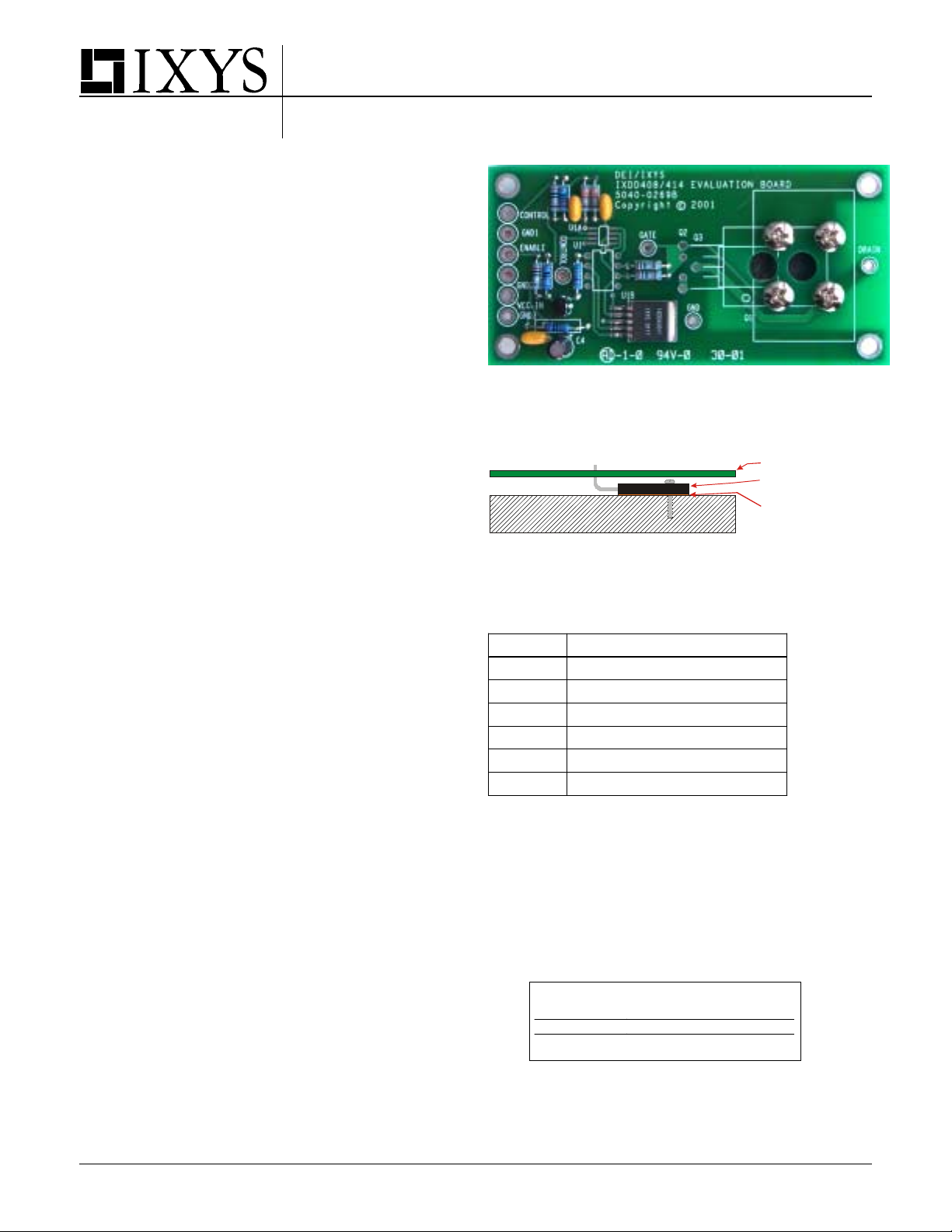
Figure 1 is a photograph of the IXDD408/414 Evaluation
Board loaded with an IXDD408YI TO-263 driver and a SOT227 MOSFET. The low level inputs are shown on the left side
of the board. Control is a TTL high true input which controls
the on or off state of the power switch Q1, Q2, or Q3. Enable
is a low true input, which controls the Tri-State output. VCC-IN
is the low voltage, (8-25V) power input, (see Figure 3 below).
Figure 2 illustrates the MOSFET mounting of a TO-220, TO247, or TO-264 device. The MOSFET is mounted on the back
side of the PCB. A large through hole is provided so that the
device can be attached to a heat sink. The SOT-227 (shown
in the photograph) is mounted in a similar manner.
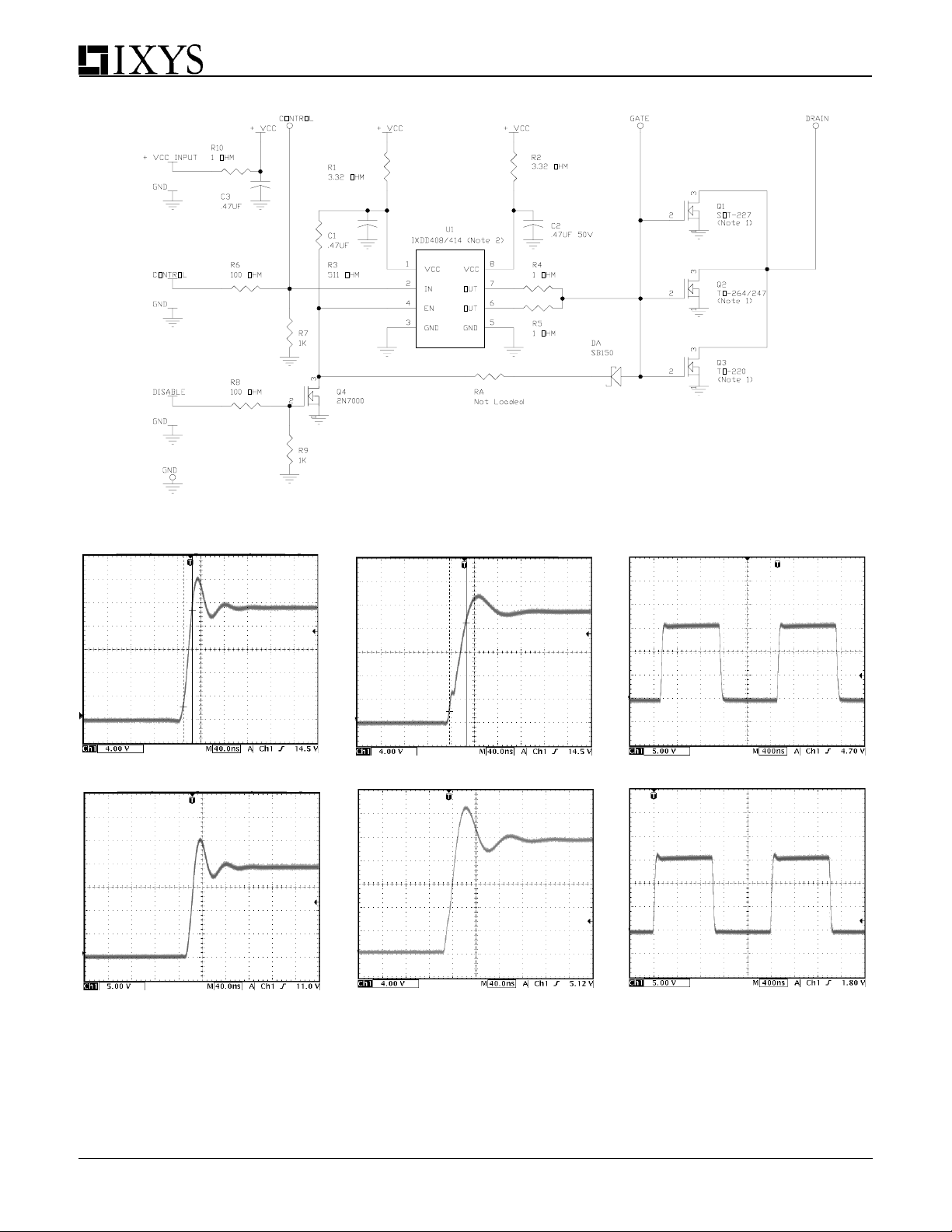
Circuit Operation
The schematic diagram for the evaluation board is shown in
Figure 4. The control gate is applied to R6 then on the input
pin 2 of the IC. This signal input is followed in time by the
output pins 7 and 6. Pins 1 and 8 are attached to +VCC via a
de-coupling network comprised of R1, C1 and R2, C2. Pins 4
and 5 are attached to the circuit ground plane. This is the
preferred arrangement of the bypassing for the Vcc input
power. The enable pin 3 is attached to the drain of Q4. This
device is used to level translate and provide an invert function
for the Tri-State mode. The drain of Q4 is also attached to the
gate of the MOSFET thru RA and DA. In the Tri-State mode
the turn-off time of the power MOSFET is determined by the
time constant of the input gate capacitance C
of the resistor RA. See the IXDD408 and IXDD414 data
sheets for additional information on this mode of operation.
The U1 output is available at pins 7 and 6. These are
attached to the MOSFET via the two one-Ohm resistors R4
and R5. The values of these resistors may be changed to
optimize the performance of the specific device being driven.
There are three test points on the board: Control, Gate and
Drain. These allow the user to easily attach an oscilloscope
probe and the associated ground to the circuit to verify
performance.
and the value
iss
Figure 1 - EVDD408/EVDD414 Evaluation Board
SOT-227 Device Installed For Illustration Purposes Only
Evaluation PCB
TO-220, TO-247,
TO-264, or SOT-227
Heat Sink
Figure 2 - EVDD408/EVDD414 Side View Showing Power
Device Installed In A High-Power Configuration
INPUT FUNCTION
CONTROL Control Input - 3V into 1K Ohms
GND1 Ground 1
ENABLE LOW = True, HIGH = Tri-State Mode
GND2 Ground 2
VCC-IN VCC input - 8V to 25V
GND 3 Ground 3
Figure 3 - Input Pin-Out Table
Kapton Insulator
The EVDD408/EVDD414 are supplied with either IXDD408YI
or IXDD414YI 5-Pin TO-263 devices installed. To use the
evaluation board with a different package type, the installed
device must be removed, and the new device installed in the
appropriate location.
Ordering Information
Part Number Installed Device
EVDD408 IXDD408YI 5-Pin TO-263
EVDD414 IXDD414YI 5-Pin TO-263
Copyright © IXYS CORPORATION 2001
First Release
EVDD408/EVDD414
Figure 4 - EVDD408/EVDD414 Schematic Diagram
NOTES: 1) The schematic shows all three output switches, however only one device can be installed at any one time.
2) The pin-out for device U1 reflects the 8-pin package types (PI and SI). See the IXDD408 and IXDD414 data sheet
for the pin-out of the TO-220 and TO-263 (YI and CI) packages.
Figure 5 - IXDD408 14ns Gate Rise Time,
CL=2500pF
Figure 8 - IXDD414 11ns Gate Rise Time
CL=2500pF
Figure 6 - IXDD408 28ns Gate Rise Time,
CL=10000pF
Figure 9 - IXDD414 18ns Gate Rise Time
CL=10000pF, R4 & R5=0Ω
Figure 7 - IXDD408 Typical Waveform
F=500KHz, CL=10000pF
Figure 10 - IXDD414 Typical Waveform
F=500KHz, CL=10000pF
NOTE: The capacitive loads used to generate the waveforms above are fixed value ceramic components. All
measurements are made at the GATE test point.
IXYS Corporation
3540 Bassett St; Santa Clara, CA 95054
Tel: 408-982-0700; Fax: 408-496-0670
e-mail: sales@ixys.net
IXYS Semiconductor GmbH
Edisonstrasse15 ; D-68623; Lampertheim
Tel: +49-6206-503-0; Fax: +49-6206-503627
e-mail: marcom@ixys.de
2
Directed Energy, Inc.
An IXYS Company
2401 Research Blvd. Ste. 108
Ft. Collins, CO 80526
Tel: 970-493-1901; Fax: 970-493-1903
e-mail: deiinfo@directedenergy.com
Doc #9200-0231 Rev 1
 Loading...