

DEI DEIC420 Datasheet
DEIC420
20 Ampere Low-Side Ultrafast RF MOSFET Driver
Features
• Built using the advantages and compatibility
of CMOS and IXYS HDMOSTM processes
• Latch-Up Protected
• High Peak Output Current: 20A Peak
• Wide Operating Range: 8V to 30V
• Rise And Fall Times of <4ns
• Minimum Pulse Width Of 8ns
• High Capacitive Load
Drive Capability: 4nF in <4ns
• Matched Rise And Fall Times
• 32ns Input To Output Delay Time
• Low Output Impedance
• Low Quiescent Supply Currentt
Applications
• Driving RF MOSFETs
• Class D or E Switching Amplifier Drivers
• Multi MHz Switch Mode Power Supplies (SMPS)
• Pulse Generators
• Acoustic Transducer Drivers
• Pulsed Laser Diode Drivers
• DC to DC Converters
• Pulse Transformer Driver
Description
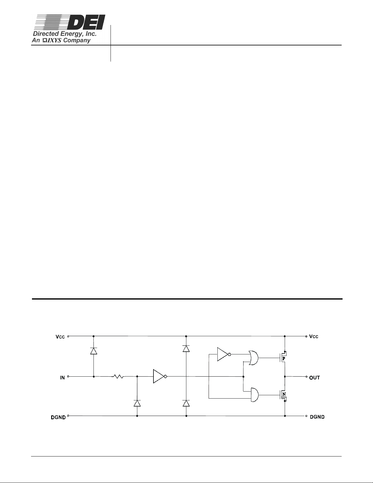
TheDEIC420 is a CMOS high speed high current gate
driver specifically designed to drive MOSFETs in Class D
and E HF RF applications at up to 45MHz, as well as
other applications requiring ultrafast rise and fall times or
short minimum pulse widths. The DEIC420 can source
and sink 20A of peak current while producing voltage rise
and fall times of less than 4ns, and minimum pulse
widths of 8ns. The input of the driver is compatible with
TTL or CMOS and is fully immune to latch up over the
entire operating range. Designed with small internal
delays, cross conduction/current shoot-through is
virtually eliminated in the DEIC420. Its features and wide
safety margin in operating voltage and power make the
DEIC420 unmatched in performance and value.
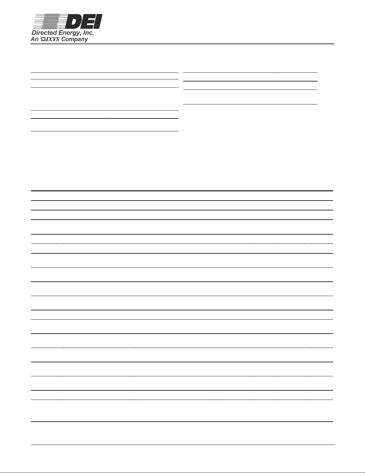
The DEIC420 is packaged in DEI's low inductance RF
package incorporating DEI's patented
techniques to minimize stray lead inductances for
optimum switching performance. For applications that do
not require the power dissipation of the DEIC420, the
driver is also available in a 28 pin SOIC package. See
the IXDD415SI data sheet for additional information. The
DEIC420 is a surface-mount device, and incorporates
patented RF layout techniques to minimize stray lead
inductances for optimum switching performance.
(1)
DEI U.S. Patent #4,891,686
(1)
RF layout
Figure 1 - DEIC420 Functional Diagram
Copyright © DIRECTED ENERGY, INC. 2001
First Release
DEIC420
Absolute Maximum Ratings
Parameter Value
Supply Voltage 30V
All Other Pins
Power Dissipation
T
T
Storage Temperat ure
Soldering L ead Temperature
(10 seconds maximum)
AMBIENT
≤25 oC
CASE
≤25 oC
-0.3V to VCC + 0.3V
2W
100W
-65oC to 150oC
300oC
Electrical Characteristics
Unless otherwise noted, TA = 25 oC, 8V ≤ V
All voltage measurements with respect to DGND. DEIC420 configured as described in Test Conditions.
Symbol Parameter Test Conditions Min Typ Max Units
V
IH
High input voltage 3.5 V
VIL Low input voltage 0.8 V
VIN Input voltage range -5 V
IIN Input current
VOH High output voltage V
VOL Low output voltage 0.025 V
ROH Output resistance
@ Output high
ROL Output resistance
@ Output Low
I
Peak output current VCC = 15V
PEAK
I
Continuous output
DC
current
f
Maximum frequency CL=4nF Vcc=15V 45 MHz
MAX
tR Rise time
tF Fall time
t
On-time propagation
ONDLY
delay
t
Off-time propagation
OFFDLY
delay
P
Minimum pulse width FWHM CL=1nF Vcc=15V
Wmin
(1)
C
(1)
C
(1)
(1)
VCC Power supply voltage 8 15 30 V
ICC Power supply current V
(1)
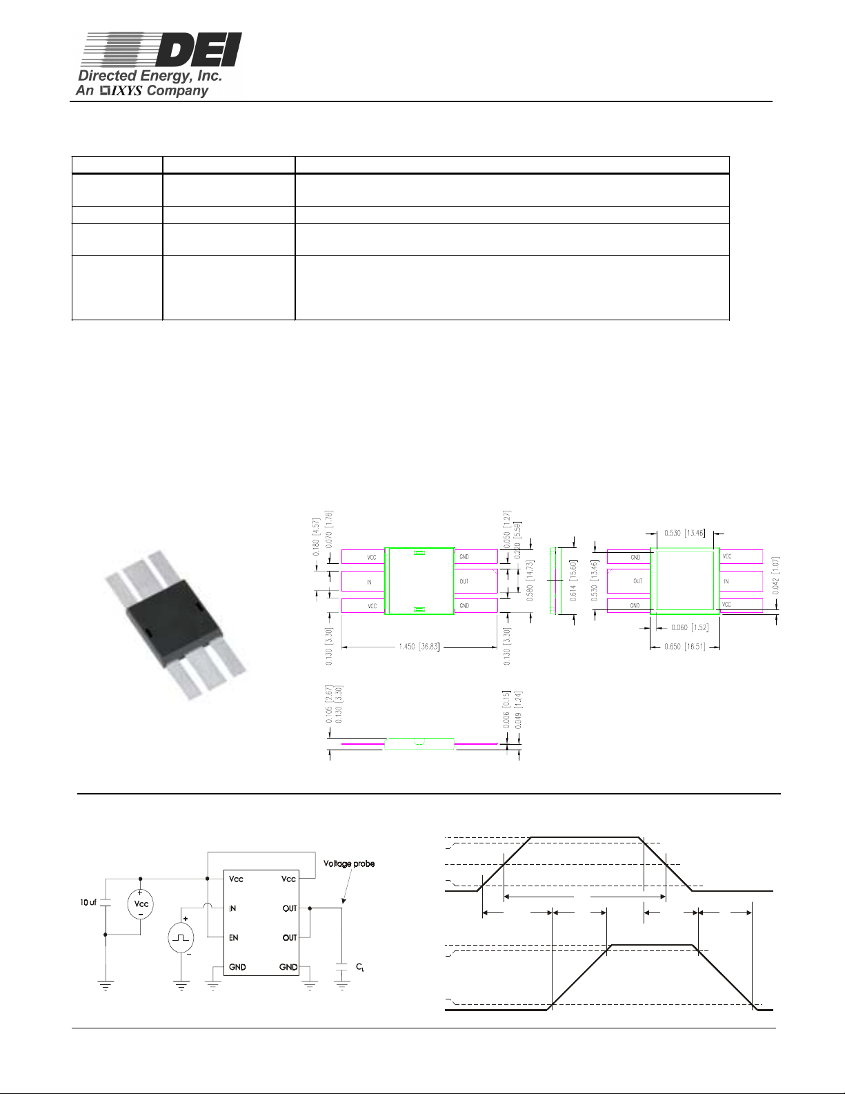
Refer to Figures 3a and 3b
Specifications Subject To Change Without Notice
≤ 30V .
CC
0V ≤ V
IN
V
≤
I
= 10mA, V
OUT
I
= 10mA, V
OUT
4 A
=1nF Vcc=15V VOH=2V to 12V
L
=4nF Vcc=15V VOH=2V to 12V
C
L
=1nF Vcc=15V VOH=12V to 2V
L
=4nF Vcc=15V VOH=12V to 2V
C
L
C
=4nF Vcc=15V 32 38 ns
L
C
=4nF Vcc=15V 29 35 ns
L
+3V to +3V C
= 3.5V
IN
= 0V
V
IN
= + VCC
V
IN
Parameter Value
Maximum Junction Temperature
Operating Temperature Range
Thermal Impedance (Junction To Case)
θ
JC
CC
= 15V
CC
= 15V 0.4 0.6
CC
-10 10
- .025 V
CC
0.4 0.6
150oC
-40oC to 85oC
0.13oC/W
+ 0.3 V
CC
20 A
3
ns
4
3
ns
3.5
=1nF Vcc=15V
L
8
9
ns
1 0 3
10
10
A
µ
Ω
Ω
ns
ns
ns
mA
A
µ
A
µ
2
DEIC420
Lead Description - DEIC420
SYMBOL FUNCTION DESCRIPTION
VCC Supply Voltage
IN Input Input signal-TTL or CM OS compatible.
OUT Output
GND Power Ground
Note 1: Operating the device beyond parameters with listed “absolute maximum ratings” may cause permanent
damage to the device. Typical values indicate conditions for which the device is intended to be functional, but do not
guarantee specific performance limits. The guaranteed specifications apply only for the test conditions listed.
Exposure to absolute maximum rated conditions for extended periods may affect device reliability.
CAUTION: These devices are sensitive to electrostatic discharge; follow proper ESD procedures
when handling and assembling this component.
Figure 2 - DEIC420 Package Photo And Outline
Positiv e power-supply vol tage input. These leads provide power to
the entire c hip. The range for this voltage is from 8V t o 30V .
Driver Output. For application purposes, this lead is connected,
directly to the Gate of a MOSFET
The system ground l eads. Internal ly c onnected to all circuit ry, these
leads provide ground reference for the entire chip. These leads
should be connected to a low noise analog ground plane for
optim um perf ormance.
Figure 3a - Characteristics Test Diagram
V
IN
Figure 3b - Timing Diagram
5V
90%
INPUT
2.5V
10%
0V
t
ONDLY
Vcc
90%
OUTPUT
10%
0V
3
PW
MIN
t
R
t
OFFDLY
F
t
 Loading...