

Page 1

AlphaServer 8200/8400
System Technical Manual
Order Number EK–T8030–TM. A01
The Digital AlphaServer 8200 and 8400 systems are designed around the
DECchip 21164 CPU. The TLSB is the system bus that supports nine nodes in
the 8400 system and five nodes in the 8200 system. The AlphaServer 8400 can
be configured with up to six single or dual processor CPU modules (KN7CC),
seven memory modules (MS7CC), and three I/O modules (KFTHA and
KFTIA). One slot is dedicated to I/O and is normally occupied by the integrated I/O module (KFTIA) that supports PCI bus, XMI, and Futurebus+
adapters. All other nodes can be interchangeably configured for CPU or memory modules. The AlphaServer 8200 can be configured with up to three CPU
modules, three memory modules, and three I/O modules.
digital equipment corporation
maynard, massachusetts
Page 2

First Printing, May 1995
The information in this document is subject to change without notice and should not be construed as a commitment by Digital Equipment Corporation.
Digital Equipment Corporation assumes no responsibility for any errors that may appear in this document.
The software, if any, described in this document is furnished under a license and may be used or copied only
in accordance with the terms of such license. No responsibility is assumed for the use or reliability of software or equipment that is not supplied by Digital Equipment Corporation or its affiliated companies.
Copyright © 1995 by Digital Equipment Corporation.
All Rights Reserved.
Printed in U.S.A.
The following are trademarks of Digital Equipment Corporation: AlphaGeneration, AlphaServer, DEC,
DECchip, DEC LANcontroller, OpenVMS, StorageWorks, VAX, the AlphaGeneration logo, and the DIGITAL
logo.
OSF/1 is a registered trademark of the Open Software Foundation, Inc. Prestoserve is a trademark of Legato
Systems, Inc. UNIX is a registered trademark in the U.S. and other countries, licensed exclusively through
X/Open Company Ltd.
FCC NOTICE: The equipment described in this manual generates, uses, and may emit radio frequency energy. The equipment has been type tested and found to comply with the limits for a Class A computing device pursuant to Subpart J of Part 15 of FCC Rules, which are designed to provide reasonable protection
against such radio frequency interference when operated in a commercial environment. Operation of this
equipment in a residential area may cause interference, in which case the user at his own expense may be
required to take measures to correct the interference.
Page 3

Contents
Preface ............................................................................................................................................ xv
Chapter 1 Overview
1.1 Configuration ................................................................................................................ 1-1
1.2 Bus Architecture ........................................................................................................... 1-2
1.3 CPU Module .................................................................................................................. 1-3
1.3.1 DECchip 21164 ...................................................................................................... 1-3
1.3.2 Backup Cache ......................................................................................................... 1-4
1.3.3 TLSB Interface ....................................................................................................... 1-4
1.3.4 Console Support Hardware.................................................................................... 1-4
1.4 Memory Module ............................................................................................................ 1-4
1.5 I/O Architecture ............................................................................................................ 1-5
1.6 Software.........................................................................................................................1-6
1.6.1 Console .................................................................................................................... 1-6
1.6.2 OpenVMS Alpha ..................................................................................................... 1-7
1.6.3 Digital UNIX...........................................................................................................1-7
1.6.4 Diagnostics..............................................................................................................1-7
1.6.4.1 ROM-Based Diagnostics .................................................................................. 1-7
1.6.4.2 Loadable Diagnostic Execution Environment ............................................... 1-8
1.6.4.3 Online Exercisers ............................................................................................. 1-8
Chapter 2 TLSB Bus
2.1 Overview........................................................................................................................2-1
2.1.1 Transactions ........................................................................................................... 2-2
2.1.2 Arbitration .............................................................................................................. 2-2
2.1.3 Cache Coherency Protocol...................................................................................... 2-2
2.1.4 Error Handling ....................................................................................................... 2-2
2.1.5 TLSB Signal List .................................................................................................... 2-3
2.2 Operation.......................................................................................................................2-5
2.2.1 Physical Node ID .................................................................................................... 2-5
2.2.2 Virtual Node Identification .................................................................................... 2-6
2.2.3 Address Bus Concepts ............................................................................................ 2-6
2.2.3.1 Memory Bank Addressing Scheme ................................................................. 2-8
2.2.3.2 CSR Addressing Scheme.................................................................................. 2-8
2.2.3.3 Memory Bank Address Decoding .................................................................... 2-9
2.2.3.4 Bank Available Status ................................................................................... 2-11
2.2.3.5 Address Bus Sequencing................................................................................ 2-11
2.2.4 Address Bus Arbitration ...................................................................................... 2-12
2.2.4.1 Initiating Transactions .................................................................................. 2-12
2.2.4.2 Distributed Arbitration.................................................................................. 2-12
iii
Page 4

2.2.4.3 Address Bus Transactions ............................................................................. 2-12
2.2.4.4 Module Transactions...................................................................................... 2-12
2.2.4.5 Address Bus Priority...................................................................................... 2-12
2.2.4.6 Address Bus Request ..................................................................................... 2-13
2.2.4.7 Asserting Request .......................................................................................... 2-13
2.2.4.8 Early Arbitration ........................................................................................... 2-13
2.2.4.9 False Arbitration Effect on Priority .............................................................. 2-14
2.2.4.10 Look-Back-Two............................................................................................... 2-14
2.2.4.11 Bank Available Transition ............................................................................ 2-14
2.2.4.12 Bank Collision ................................................................................................ 2-15
2.2.4.13 Bank Lock and Unlock................................................................................... 2-15
2.2.4.14 CSR Bank Contention.................................................................................... 2-15
2.2.4.15 Command Acknowledge................................................................................. 2-16
2.2.4.16 Arbitration Suppress ..................................................................................... 2-16
2.2.5 Address Bus Cycles .............................................................................................. 2-16
2.2.6 Address Bus Commands ...................................................................................... 2-17
2.2.7 Data Bus Concepts ............................................................................................... 2-18
2.2.7.1 Data Bus Sequencing..................................................................................... 2-18
2.2.7.2 Hold................................................................................................................. 2-18
2.2.7.3 Back-to-Back Return Data ............................................................................ 2-19
2.2.7.4 Back-to-Back Return with HOLD ................................................................. 2-19
2.2.7.5 CSR Data Sequencing.................................................................................... 2-19
2.2.8 Data Bus Functions.............................................................................................. 2-19
2.2.8.1 Data Return Format ...................................................................................... 2-19
2.2.8.2 Sequence Numbers......................................................................................... 2-20
2.2.8.3 Sequence Number Errors .............................................................................. 2-20
2.2.8.4 Data Field....................................................................................................... 2-20
2.2.8.5 Data Wrapping............................................................................................... 2-20
2.2.8.6 ECC Coding .................................................................................................... 2-21
2.2.8.7 ECC Error Handling ...................................................................................... 2-22
2.2.8.8 TLSB_DATA_VALID ..................................................................................... 2-22
2.2.8.9 TLSB_SHARED ............................................................................................. 2-22
2.2.8.10 TLSB_DIRTY ................................................................................................. 2-23
2.2.8.11 TLSB_STATCHK ........................................................................................... 2-23
2.2.9 Miscellaneous Bus Signals................................................................................... 2-24
2.3 CSR Addressing .......................................................................................................... 2-25
2.3.1 CSR Address Space Regions ................................................................................ 2-26
2.3.2 TLSB Mailboxes.................................................................................................... 2-30
2.3.3 Window Space I/O................................................................................................. 2-32
2.3.3.1 CSR Write Transactions to Remote I/O Window Space............................... 2-32
2.3.3.2 CSR Read Transactions to Remote I/O Window Space................................ 2-32
2.4 TLSB Errors ................................................................................................................ 2-33
2.4.1 Error Categories ................................................................................................... 2-34
2.4.1.1 Hardware Recovered Soft Errors ................................................................. 2-34
2.4.1.2 Software Recovered Soft Errors .................................................................... 2-34
2.4.1.3 Hard Errors .................................................................................................... 2-34
2.4.1.4 System Fatal Errors....................................................................................... 2-34
2.4.2 Error Signals......................................................................................................... 2-35
2.4.3 Address Bus Errors .............................................................................................. 2-35
2.4.3.1 Transmit Check Errors.................................................................................. 2-35
2.4.3.2 Command Field Parity Errors....................................................................... 2-36
2.4.3.3 No Acknowledge Errors ................................................................................. 2-36
2.4.3.4 Unexpected Acknowledge .............................................................................. 2-37
2.4.3.5 Bank Lock Error............................................................................................. 2-37
2.4.3.6 Bank Available Violation Error..................................................................... 2-37
2.4.3.7 Memory Mapping Register Error .................................................................. 2-38
iv
Page 5

2.4.3.8 Multiple Address Bus Errors......................................................................... 2-38
2.4.3.9 Summary of Address Bus Errors .................................................................. 2-38
2.4.4 Data Bus Errors.................................................................................................... 2-39
2.4.4.1 Single-Bit ECC Errors ................................................................................... 2-40
2.4.4.2 Double-Bit ECC Errors .................................................................................. 2-40
2.4.4.3 Illegal Sequence Errors.................................................................................. 2-40
2.4.4.4 SEND_DATA Timeout Errors ....................................................................... 2-40
2.4.4.5 Data Status Errors......................................................................................... 2-41
2.4.4.6 Transmit Check Errors.................................................................................. 2-41
2.4.4.7 Multiple Data Bus Errors.............................................................................. 2-41
2.4.4.8 Summary of Data Bus Errors........................................................................ 2-42
2.4.5 Additional Status.................................................................................................. 2-42
2.4.6 Error Recovery...................................................................................................... 2-43
2.4.6.1 Read Errors .................................................................................................... 2-43
2.4.6.2 Write Errors ................................................................................................... 2-45
Chapter 3 CPU Module
3.1 Major Components ........................................................................................................ 3-1
3.1.1 DECchip 21164 Processor ...................................................................................... 3-2
3.1.2 MMG ...................................................................................................................... 3-3
3.1.3 ADG ........................................................................................................................ 3-3
3.1.4 DIGA ...................................................................................................................... 3-3
3.1.5 B-Cache .................................................................................................................. 3-4
3.2 Console........................................................................................................................... 3-4
3.2.1 Serial ROM Port ..................................................................................................... 3-5
3.2.2 Directly Addressable Console Hardware .............................................................. 3-5
3.3 CPU Module Address Space ......................................................................................... 3-6
3.3.1 Memory Space......................................................................................................... 3-7
3.3.2 I/O Space ................................................................................................................. 3-8
3.3.2.1 I/O Window Space ............................................................................................ 3-8
3.3.2.2 TLSB CSR Space ............................................................................................. 3-8
3.3.2.3 Gbus Space ....................................................................................................... 3-9
3.4 CPU Module Window Space Support......................................................................... 3-10
3.4.1 Window Space Reads............................................................................................ 3-10
3.4.2 Window Space Writes........................................................................................... 3-10
3.4.3 Flow Control ......................................................................................................... 3-10
3.4.4 PCI Accesses ......................................................................................................... 3-11
3.4.4.1 Sparse Space Reads and Writes .................................................................... 3-12
3.4.4.2 Dense Space Reads and Writes ..................................................................... 3-13
3.5 CPU Module Errors ................................................................................................... 3-14
3.5.1 Error Categories ................................................................................................... 3-14
3.5.1.1 Soft Errors ...................................................................................................... 3-14
3.5.1.2 Hard Errors .................................................................................................... 3-14
3.5.1.3 Faults.............................................................................................................. 3-15
3.5.1.4 Nonacknowledged CSR Reads....................................................................... 3-16
3.5.2 Address Bus Errors ............................................................................................. 3-16
3.5.2.1 Transmit Check Errors.................................................................................. 3-17
3.5.2.2 Command Field Parity Errors....................................................................... 3-17
3.5.2.3 No Acknowledge Errors ................................................................................. 3-18
3.5.2.4 Unexpected Acknowledge Error .................................................................... 3-18
3.5.2.5 Memory Mapping Register Error .................................................................. 3-18
3.5.3 Data Bus Errors.................................................................................................... 3-18
3.5.4 Multiple Errors ..................................................................................................... 3-19
v
Page 6

Chapter 4 Memory Subsystem
4.1 Internal Cache............................................................................................................... 4-1
4.1.1 Instruction Cache ................................................................................................... 4-1
4.1.2 Data Cache.............................................................................................................. 4-1
4.1.3 Second-Level Cache ................................................................................................ 4-2
4.2 Backup Cache................................................................................................................ 4-2
4.2.1 Cache Coherency .................................................................................................... 4-2
4.2.2 B-Cache Tags .......................................................................................................... 4-3
4.2.3 Updates and Invalidates ........................................................................................ 4-4
4.2.4 Duplicate Tags ........................................................................................................ 4-4
4.2.5 B-Cache States........................................................................................................ 4-4
4.2.6 B-Cache State Changes ......................................................................................... 4-5
4.2.7 Victim Buffers......................................................................................................... 4-6
4.2.8 Lock Registers......................................................................................................... 4-6
4.2.9 Cache Coherency on Processor Writes .................................................................. 4-8
4.2.10 Memory Barriers .................................................................................................... 4-9
4.3 Main Memory ................................................................................................................ 4-9
4.3.1 Major Sections ...................................................................................................... 4-10
4.3.1.1 Control Address Interface ............................................................................. 4-11
4.3.1.2 Memory Data Interface ................................................................................. 4-11
4.3.1.3 DRAM Arrays................................................................................................. 4-12
4.3.2 Memory Organization .......................................................................................... 4-13
4.3.3 Refresh .................................................................................................................. 4-16
4.3.4 Transactions ......................................................................................................... 4-16
4.3.5 ECC Protection ....................................................................................................... 2-2
4.3.6 Self-Test ................................................................................................................ 4-16
4.3.6.1 Self-Test Modes .............................................................................................. 4-17
4.3.6.2 Self-Test Error Reporting .............................................................................. 4-18
4.3.6.3 Self-Test Operation ........................................................................................ 4-18
4.3.6.4 Self-Test Performance.................................................................................... 4-19
Chapter 5 Memory Interface
5.1 Control Address Interface............................................................................................. 5-1
5.1.1 TLSB Control.......................................................................................................... 5-1
5.1.1.1 Memory Bank State Machine........................................................................ 2-11
5.1.1.2 CSR State Machine ........................................................................................ 2-12
5.1.1.3 TLSB Input Latches......................................................................................... 2-5
5.1.1.4 TLSB Bus Monitor ........................................................................................... 2-6
5.1.1.5 TLSB Command Decode .................................................................................. 2-6
5.1.1.6 TLSB Bank Match Logic.................................................................................. 2-8
5.1.1.7 TLSB Parity Check .......................................................................................... 2-8
5.1.1.8 TLSB Sequence Control................................................................................... 2-9
5.1.1.9 TLSB Bank Available Flags .......................................................................... 2-11
5.1.2 DRAM Control ...................................................................................................... 2-12
5.1.3 Address/RAS Decode Logic .................................................................................. 2-12
5.1.3.1 128MB/512MB Memory Module Addressing................................................ 2-12
5.1.3.2 256MB/1024MB Memory Module Addressing.............................................. 2-13
5.1.3.3 512MB/2048MB Memory Module Addressing.............................................. 2-13
5.2 Memory Data Interface................................................................................................. 5-9
5.2.1 Data Path Logic .................................................................................................... 2-14
5.2.2 Write Data Input Logic ........................................................................................ 2-14
5.2.2.1 Write Data Buffer ............................................................................................ 5-9
5.2.2.2 Write Data Path ECC Algorithm .................................................................. 2-15
vi
Page 7

5.2.2.3 CSR Write Data ECC Check ......................................................................... 5-10
5.2.2.4 Forcing Write Errors for Diagnostics............................................................ 2-15
5.2.2.5 Write Data Out Selection .............................................................................. 2-15
5.2.3 Read Data Output Logic....................................................................................... 2-16
5.2.3.1 Read Data Buffers.......................................................................................... 2-16
5.2.3.2 Read Data Path ECC Algorithm ................................................................... 5-11
5.2.3.3 CSR Read Data ECC...................................................................................... 2-17
5.2.4 MDI Error Detection and Correction Logic......................................................... 2-17
5.3 CSR Interface .............................................................................................................. 5-13
5.3.1 CTL CSR Functions.............................................................................................. 2-18
5.3.1.1 TLSB CSR Control ......................................................................................... 2-18
5.3.1.2 MAI CSR Sequencer............................................................................... 5-15
5.3.1.3 CSR Multiplexing........................................................................................... 2-19
5.3.1.4 CSRCA Parity ................................................................................................ 2-19
5.3.2 MDI CSR Functions ............................................................................................. 2-19
5.3.2.1 MDI CSR Sequencer ...................................................................................... 2-19
5.3.2.2 Merge Register ............................................................................................... 2-20
5.3.2.3 CSR Multiplexing........................................................................................... 2-20
5.3.2.4 CSRCA Parity ................................................................................................ 2-20
Chapter 6 I/O Port
6.1 Configuration ................................................................................................................ 6-2
6.2 I/O Port Main Components........................................................................................... 6-2
6.3 I/O Port Transactions ................................................................................................... 6-3
6.3.1 Mailbox Transactions ............................................................................................. 6-5
6.3.2 I/O Window Space Transactions ............................................................................ 6-7
6.3.2.1 CSR Write Transactions to I/O Window Space .............................................. 6-7
6.3.2.2 CSR Read Transactions to I/O Window Space ............................................... 6-8
6.3.3 Interrupt Transactions........................................................................................... 6-8
6.3.3.1 Remote Bus Interrupts .................................................................................... 6-8
6.3.3.2 I/O Port Generated Error Interrupts .............................................................. 6-9
6.3.4 DMA Read Transactions ...................................................................................... 6-10
6.3.5 DMA Interlock Read Transactions ...................................................................... 6-10
6.3.6 DMA Write Transactions ..................................................................................... 6-11
6.3.6.1 DMA Unmasked Write .................................................................................. 6-12
6.3.6.2 DMA Masked Write Request to Memory ...................................................... 6-12
6.3.7 Extended NVRAM Write Transactions ............................................................... 6-13
6.4 Addressing................................................................................................................... 6-14
6.4.1 Accessing Remote I/O Node CSRs Through Mailboxes ...................................... 6-14
6.4.2 Accessing Remote I/O Node CSRs Through Direct I/O Window Space ............. 6-15
6.4.2.1 Sparse Address Space Reads ......................................................................... 6-15
6.4.2.2 Sparse Address Space Writes ........................................................................ 6-17
6.4.3 Dense Address Space Transactions ..................................................................... 6-20
6.5 TLSB Interface............................................................................................................ 6-23
6.5.1 Transactions ......................................................................................................... 6-23
6.5.1.1 DMA Transactions ......................................................................................... 6-24
6.5.1.2 Interrupt Transactions ................................................................................. 6-26
6.5.1.3 CSR Transactions .......................................................................................... 6-28
6.5.2 TLSB Arbitration.................................................................................................. 6-30
6.5.2.1 Node 8 I/O Port Arbitration Mode Selection................................................. 6-31
6.5.2.2 Read-Modify-Write......................................................................................... 6-33
6.5.2.3 Bank Collision Effect on Priority .................................................................. 6-34
6.5.2.4 Look-Back-Two............................................................................................... 6-34
6.5.2.5 Arbitration Suppress ..................................................................................... 6-34
vii
Page 8

6.5.3 Error Detection Schemes ..................................................................................... 6-34
6.6 Hose Interface ............................................................................................................. 6-35
6.6.1 Hose Protocol ....................................................................................................... 6-35
6.6.2 Window Space Mapping ....................................................................................... 6-36
6.6.2.1 Sparse Address Mapping ............................................................................... 6-37
6.6.2.2 Dense Address Mapping ................................................................................ 6-37
6.6.3 Hose Signals ......................................................................................................... 6-37
6.6.4 Hose Packet Specifications................................................................................... 6-39
6.6.4.1 Down Hose Packet Specifications ................................................................. 6-39
6.6.4.2 Up Hose Packet Specifications ...................................................................... 6-52
6.6.5 Hose Errors ........................................................................................................... 6-65
6.7 I/O Port Error Handling ............................................................................................. 6-66
6.7.1 Soft TLSB Errors Recovered by Hardware ......................................................... 6-66
6.7.2 Hard TLSB Errors ................................................................................................ 6-66
6.7.3 System Fatal Errors ............................................................................................. 6-66
6.7.4 Hard Internal I/O Port Errors ............................................................................. 6-66
6.7.5 Error Reporting .................................................................................................... 6-67
6.7.5.1 TLSB_DATA_ERROR.................................................................................... 6-67
6.7.5.2 TLSB_FAULT ................................................................................................ 6-68
6.7.6 IPL 17 Error Interrupts ....................................................................................... 6-69
6.7.7 Address Bus Errors .............................................................................................. 6-70
6.7.7.1 TLSB Address Transmit Check Errors......................................................... 6-70
6.7.7.2 Address Bus Parity Errors ............................................................................ 6-71
6.7.7.3 No Acknowledge Errors ................................................................................. 6-71
6.7.7.4 Unexpected Acknowledge .............................................................................. 6-71
6.7.7.5 Bank Busy Violation ...................................................................................... 6-71
6.7.7.6 Memory Mapping Register Error .................................................................. 6-71
6.7.8 Data Bus Errors.................................................................................................... 6-72
6.7.8.1 Single-Bit ECC Errors ................................................................................... 6-72
6.7.8.2 Double-Bit ECC Errors .................................................................................. 6-72
6.7.8.3 Illegal Sequence Errors.................................................................................. 6-73
6.7.8.4 SEND_DATA Timeout Errors ....................................................................... 6-73
6.7.8.5 Data Status Errors......................................................................................... 6-73
6.7.8.6 Transmit Check Errors.................................................................................. 6-74
6.7.8.7 Multiple Data Bus Errors.............................................................................. 6-74
6.7.9 Additional TLSB Status ....................................................................................... 6-74
6.7.10 Hard I/O Port Errors ............................................................................................ 6-75
6.7.10.1 Up Hose Errors...............................................................................................6-75
6.7.10.2 Up Turbo Vortex Errors ................................................................................ 6-75
6.7.10.3 Down Turbo Vortex Errors ............................................................................ 6-76
6.7.11 Miscellaneous I/O Port Errors ............................................................................. 6-77
6.7.11.1 CSR Bus Parity Errors .................................................................................. 6-77
6.7.11.2 Unexpected Mailbox Status Packet .............................................................. 6-77
6.7.11.3 ICR and IDR Internal Illogical Errors.......................................................... 6-77
6.7.11.4 Hose Status Change Errors........................................................................... 6-78
6.8 KFTIA Overview ......................................................................................................... 6-78
6.8.1 Integrated I/O Section ......................................................................................... 6-80
6.8.1.1 PCI Interface .................................................................................................. 6-81
6.8.1.2 SCSI Ports ..................................................................................................... 6-82
6.8.1.3 Ethernet Ports................................................................................................ 6-83
6.8.1.4 Optional NVRAM Daughter Card ................................................................ 6-83
6.8.2 Integrated I/O Section Transactions ................................................................... 6-83
6.8.2.1 DMA Transactions ......................................................................................... 6-83
6.8.2.2 Mailbox Transaction ...................................................................................... 6-84
6.8.2.3 CSR Transactions ......................................................................................... 6-84
6.8.2.4 Interrupt Transactions .................................................................................. 6-84
viii
Page 9

Chapter 7 System Registers
7.1 Register Conventions .................................................................................................... 7-1
7.2 Register Address Mapping ........................................................................................... 7-2
7.3 TLSB Registers ............................................................................................................. 7-4
TLDEV—Device Register ...................................................................................... 7-5
TLBER—Bus Error Register ................................................................................. 7-7
TLCNR—Configuration Register ........................................................................ 7-14
TLVID—Virtual ID Register ............................................................................... 7-19
TLMMRn—Memory Mapping Registers ............................................................ 7-21
TLFADRn—Failing Address Registers .............................................................. 7-24
TLESRn—Error Syndrome Registers ................................................................ 7-26
TLILIDn—Interrupt Level IDENT Registers .................................................... 7-30
TLCPUMASK—CPU Interrupt Mask Register ................................................. 7-31
TLMBPR—Mailbox Pointer Registers ................................................................ 7-32
TLIPINTR—Interprocessor Interrupt Register.................................................. 7-35
TLIOINTRn—I/O Interrupt Registers ............................................................... 7-36
TLWSDQR4-8—Window Space Decr Queue Counter Registers ....................... 7-38
TLRMDQRX—Memory Channel Decr Queue Counter Register X ...................7-39
TLRMDQR8—Memory Channel Decr Queue Counter Register 8 .................... 7-40
TLRDRD—CSR Read Data Return Data Register............................................. 7-41
TLRDRE—CSR Read Data Return Error Register ........................................... 7-42
TLMCR—Memory Control Register .................................................................... 7-43
7.4 CPU Module Registers................................................................................................ 7-44
TLDIAG—Diagnostic Setup Register ................................................................. 7-47
TLDTAGDATA—DTag Data Register ................................................................ 7-50
TLDTAGSTAT—DTag Status Register .............................................................. 7-51
TLMODCONFIG—CPU Module Configuration Register ................................. 7-52
TLEPAERR— ADG Error Register .................................................................... 7-54
TLEPDERR—DIGA Error Register ................................................................... 7-57
TLEPMERR—MMG Error Register ................................................................... 7-59
TLEP_VMG—Voltage Margining Register ......................................................... 7-62
TLINTRMASK0–1—Interrupt Mask Registers ................................................. 7-63
TLINTRSUM0–1—Interrupt Source Registers ................................................. 7-65
TLCON00,01,10,11—Console Communications Regs ........................................ 7-68
TLCON0A,0B,0C,1A,1B,1C—DIGA Comm. Test Regs ...................................... 7-69
RM_RANGE_nA,B—Memory Channel Range Regs........................................... 7-70
TLDMCMD—Data Mover Command Register ................................................... 7-72
TLDMADRA—Data Mover Source Address Register ........................................ 7-75
TLDMADRB—Data Mover Destination Address Reg ....................................... 7-76
GBUS$WHAMI..................................................................................................... 7-77
GBUS$LED0,1,2................................................................................................... 7-78
GBUS$MISCR ...................................................................................................... 7-79
GBUS$MISCW ..................................................................................................... 7-81
GBUS$TLSBRST.................................................................................................. 7-82
GBUS$SERNUM.................................................................................................. 7-83
7.5 Memory-Specific Registers ......................................................................................... 7-85
SECR—Serial EEPROM Control/Data Register ............................................... 7-86
MIR—Memory Interleave Register .................................................................... 7-87
MCR—Memory Configuration Register .............................................................. 7-89
STAIR—Self-Test Address Isolation Register ................................................... 2-24
STER—Self-Test Error Register.......................................................................... 2-24
MER—Memory Error Register ............................................................................ 7-97
MDRA—Memory Diagnostic Register A ............................................................ 2-26
MDRB—Memory Diagnostic Register B ........................................................... 7-102
STDERA,B,C,D,E—Self-Test Data Error Registers ........................................ 7-103
ix
Page 10

DDR0:3—Data Diagnostic Registers ................................................................ 7-106
7.6 I/O Port-Specific Registers........................................................................................ 7-109
RMRR0-1—Memory Channel Range Registers ................................................ 7-110
ICCMSR—I/O Control Chip Mode Select Register........................................... 7-112
ICCNSE—I/O Control Chip Node-Specific Error Reg ...................................... 7-117
ICCDR—I/O Control Chip Diagnostic Register ................................................ 7-122
ICCMTR—I/O Control Chip Mailbox Transaction Reg .................................... 7-125
ICCWTR—I/O Control Chip Window Transaction Reg.................................... 7-127
IDPNSE0–3—I/O Data Path Node-Specific Error Regs .................................. 7-128
IDPDRn—I/O Data Path Diagnostic Registers................................................. 7-133
IDPVR—I/O Data Path Vector Register .......................................................... 7-137
IDPMSR—I/O Data Path Mode Select Register ............................................... 7-138
IBR—Information Base Repair Register........................................................... 7-140
7.7 KFTIA Specific Registers.......................................................................................... 7-142
Chapter 8 Interrupts
8.1 Vectored Interrupts....................................................................................................... 8-1
8.1.1 I/O Port Interrupt Rules......................................................................................... 8-1
8.1.2 CPU Interrupt Rules .............................................................................................. 8-2
8.1.3 I/O Port Interrupt Operation ................................................................................. 8-2
8.2 Nonvectored Interrupts ................................................................................................ 8-3
8.3 I/O Interrupt Mechanism ............................................................................................. 8-3
8.3.1 TLSB Principles for Interrupts.............................................................................. 8-3
8.3.1.1 Virtual Node Identification - TLVID............................................................... 8-4
8.3.1.2 Directing Interrupts - TLCPUMASK.............................................................. 8-4
8.3.1.3 Directing Interrupts - TLINTRMASK ............................................................ 8-4
8.3.1.4 Interrupt Registers - TLIOINTR4–8............................................................... 8-4
8.3.2 Generating Interrupts............................................................................................ 8-5
8.3.3 Servicing Interrupts ............................................................................................... 8-5
8.3.4 Interprocessor Interrupts....................................................................................... 8-5
8.3.5 Module-Level Interrupts ........................................................................................ 8-6
Glossary
Figures
1-1 AlphaServer 8400 System Block Diagram.............................................................. 1-2
2-1 TLSB Memory Address Bit Mapping ...................................................................... 2-7
2-2 Address Decode....................................................................................................... 2-10
2-3 64-Bit ECC Coding Scheme ................................................................................... 2-21
2-4 TLSB CSR Address Bit Mapping .......................................................................... 2-26
2-5 TLSB CSR Space Map............................................................................................ 2-27
2-6 Mailbox Data Structure ......................................................................................... 2-30
2-7 TLRDRD Register ..................................................................................................2-33
3-1 CPU Module Simple Block Diagram .......................................................................3-2
3-2 Physical Address Space Map ................................................................................... 3-6
3-3 TLSB CSR Space Map.............................................................................................. 3-8
3-4 Gbus Map..................................................................................................................3-9
3-5 PCI Programmer’s Address....................................................................................3-11
4-1 Cache Index and Tag Mapping to Block Address (4MB)........................................ 4-3
4-2 Cache Index and Tag Mapping to Block Address (1MB)........................................ 4-3
x
Page 11

4-3 Cache Index and Tag Mapping to Block Address (16MB)...................................... 4-4
4-4 Memory Module Block Diagram ............................................................................ 4-10
4-5 Two-Way Interleave of a 128-Mbyte DRAM Array .............................................. 4-14
4-6 Interleaving Different Size Memory Modules.......................................................4-14
4-7 Eight-Way System Interleave of Four 128-Mbyte Memory Modules .................. 4-15
5-1 64-Bit ECC Coding Scheme ................................................................................... 5-10
5-2 CSR Interface Context ........................................................................................... 5-13
5-3 CSRCA Encoding.................................................................................................... 5-14
6-1 I/O Subsystem Block Diagram................................................................................. 6-1
6-2 I/O Port Block Diagram............................................................................................ 6-3
6-3 Sparse Address Space Reads ................................................................................. 6-16
6-4 Sparse Window Read Data as Presented on the TLSB ........................................ 6-16
6-5 Sparse Address Space Writes ................................................................................ 6-18
6-6 Sparse Address Space Write Data......................................................................... 6-18
6-7 Dense Address Space Transactions....................................................................... 6-20
6-8 Dense Address Space Write Data.......................................................................... 6-22
6-9 Dense Window Read Data as Presented on the TLSB .........................................6-22
6-10 Write CSR (Interrupt) Data Format ................................................................... 6-27
6-11 Minimum Latency Mode ......................................................................................6-32
6-12 Minimum Latency Mode Timing Example .........................................................6-32
6-13 Toggle 50% High/50% Low Mode......................................................................... 6-33
6-14 Mailbox Command Packet ................................................................................... 6-41
6-15 DMA Read Data Return Packet ..........................................................................6-42
6-16 DMA Read Data Return Packet with Error........................................................ 6-44
6-17 INTR/IDENT Status Return Packet ................................................................... 6-45
6-18 Sparse Window Read Command Packet ............................................................. 6-45
6-19 Sparse Window Write Command Packet ............................................................ 6-47
6-20 Dense Window Read Command Packet .............................................................. 6-48
6-21 Dense Window Write Command Packet ............................................................. 6-50
6-22 Byte Mask Field....................................................................................................6-51
6-23 Memory Channel Write Packet ........................................................................... 6-52
6-24 Mailbox Status Return Packet.............................................................................6-53
6-25 DMA Read Packet ................................................................................................6-54
6-26 Interlock Read Packet .......................................................................................... 6-56
6-27 DMA Masked Write Packet ................................................................................. 6-57
6-28 DMA Unmasked Write Packet ............................................................................6-59
6-29 INTR/IDENT Status Return Packet ................................................................... 6-60
6-30 Sparse Window Read Data Return Packet ......................................................... 6-61
6-31 Dense Window Read Data Return Packet ..........................................................6-63
6-32 Window Write Status Return Packet .................................................................. 6-64
6-33 KFTIA Connections .............................................................................................. 6-78
6-34 KFTIA Block Diagram .........................................................................................6-79
6-35 Integrated I/O Section of the KFTIA...................................................................6-81
7-1 Mailbox Data Structure ......................................................................................... 7-33
Tables
1 Digital AlphaServer 8200/8400 Documentation......................................................... xvii
2 Related Documents ....................................................................................................... xix
2-1 TLSB Bus Signals ......................................................................................................... 2-3
2-2 TLSB Physical Node Identification..............................................................................2-5
2-3 Interleave Field Values for Two-Bank Memory Modules ...........................................2-9
2-4 TLSB Address Bus Commands .................................................................................. 2-17
2-5 TLSB Data Wrapping ................................................................................................. 2-21
2-6 CSR Address Space Regions....................................................................................... 2-26
xi
Page 12

2-7 TLSB Node Base Addresses .......................................................................................2-28
2-8 TLSB CSR Address Mapping ..................................................................................... 2-29
2-9 Mailbox Data Structure .............................................................................................. 2-31
2-10 Address Bus Error Summary ..................................................................................... 2-39
2-11 Signals Covered by TLESRn Registers...................................................................... 2-39
2-12 Data Bus Error Summary .......................................................................................... 2-42
3-1 Directly Addressable Console Hardware ..................................................................... 3-6
3-2 TLSB Wrapping ...........................................................................................................3-7
3-3 CPU Module Wrapping ................................................................................................ 3-7
3-4 Decrement Queue Counter Address Assignments .................................................... 3-11
3-5 PCI Address Bit Descriptions..................................................................................... 3-12
3-6 Valid Values for Address Bits <6:5> ..........................................................................3-13
4-1 B-Cache States ..............................................................................................................4-5
4-2 State Transition Due to Processor Activity ................................................................. 4-7
4-3 State Transition Due to TLSB Activity ....................................................................... 4-8
4-4 CPU Module Response to Lock Register and Victim Buffer Address Hits ................4-8
4-5 Memory Array Capacity ............................................................................................. 4-13
4-6 Self-Test Error Registers ............................................................................................ 4-18
4-7 Self-Test Times: Normal Mode................................................................................... 4-19
4-8 Self-Test Times: Moving Inversion, No Errors Found .............................................. 4-20
5-1 TLSB Command Encoding ...........................................................................................5-3
5-2 Two Strings—128MB/512MB Row/Column Address Bit Swapping...........................5-6
5-3 Four Strings—256MB/1024MB Row/Column Address Bit Swapping........................5-7
5-4 Eight Strings—512MB/2048MB Row/Column Address Bit Swapping ...................... 5-8
5-5 Error Conditions Monitored by the MDIs.................................................................. 5-12
5-6 CSRCA Addressing ..................................................................................................... 5-15
5-7 CSRCA Data Bus Master ........................................................................................... 5-17
6-1 I/O Port Transaction Types .......................................................................................... 6-5
6-2 TLMBPR Register Map .............................................................................................. 6-15
6-3 Sparse Address Space Read Field Descriptions ........................................................ 6-17
6-4 Sparse Address Space Write Field Descriptions ....................................................... 6-19
6-5 Sparse Address Write Length Encoding.................................................................... 6-20
6-6 Dense Address Space Transaction Field Descriptions..............................................6-21
6-7 Transaction Types Supported by the I/O Port........................................................... 6-24
6-8 Wrapped Reads ...........................................................................................................6-25
6-9 I/O Adapter to Memory Write Types.......................................................................... 6-26
6-10 Down Hose Signals ..................................................................................................... 6-38
6-11 Up Hose Signals .......................................................................................................... 6-38
6-12 UPCTL<3:0> Encoding ............................................................................................... 6-39
6-13 Hose Status Signals .................................................................................................... 6-40
6-14 Down Hose Packet Type Codes .................................................................................. 6-40
6-15 Mailbox Command Packet Description......................................................................6-42
6-16 DMA Read Data Return Packet Description............................................................. 6-43
6-17 DMA Read Data Return Packet with Error Description .......................................... 6-44
6-18 INTR/IDENT Status Return Packet Description...................................................... 6-45
6-19 Sparse Window Read Command Packet Description................................................6-46
6-20 Sparse Window Write Command Packet Description...............................................6-48
6-21 Dense Window Read Command Packet Description................................................. 6-49
6-22 Dense Window Write Command Packet Description................................................ 6-51
6-23 Memory Channel Write Packet Description.............................................................. 6-53
6-24 Mailbox Status Return Packet Description............................................................... 6-54
6-25 DMA Read Packet Description................................................................................... 6-55
6-26 DMA Read Packet Sizes ............................................................................................. 6-55
6-27 Interlock Read Packet Description.............................................................................6-56
6-28 Interlock Read Packet Size......................................................................................... 6-56
6-29 DMA Masked Write Packet Description.................................................................... 6-58
xii
Page 13

6-30 DMA Masked Write Packet Sizes .............................................................................. 6-58
6-31 DMA Unmasked Write Packet Description............................................................... 6-60
6-32 INTR/IDENT Status Return Packet Description...................................................... 6-61
6-33 Sparse Window Read Data Return Packet Description............................................ 6-62
6-34 Dense Window Read Data Return Packet Description............................................. 6-63
6-35 Window Write Status Return Packet Description .................................................... 6-64
6-36 PCI 0 and PCI 1 Interrupt Priority............................................................................ 6-85
7-1 TLSB Node Space Base Addresses............................................................................... 7-3
7-2 TLSB Registers .............................................................................................................7-4
7-3 TLDEV Register Bit Definitions .................................................................................. 7-5
7-4 TLBER Register Bit Definitions...................................................................................7-8
7-5 TLCNR Register Bit Definitions ................................................................................ 7-15
7-6 TLVID Register Bit Definitions ................................................................................. 7-20
7-7 TLMMRn Register Bit Definitions............................................................................. 7-21
7-8 Interleave Field Values for Two-Bank Memory Modules .........................................7-22
7-9 Address Ranges Selected by ADRMASK Field Values ............................................. 7-23
7-10 TLFADRn Register Bit Definitions............................................................................ 7-24
7-11 TLESRn Register Bit Definitions...............................................................................7-26
7-12 TLILIDn Register Bit Definitions.............................................................................. 7-30
7-13 TLCPUMASK Register Bit Definitions ..................................................................... 7-31
7-14 TLMBPR Register Bit Definitions ............................................................................. 7-32
7-15 Mailbox Data Structure Description.......................................................................... 7-33
7-16 TLIPINTR Register Bit Definitions ........................................................................... 7-35
7-17 TLI/OINTR Register Bit Definitions..........................................................................7-36
7-18 TLRDRD Register Bit Definitions..............................................................................7-41
7-19 TLMCR Register Bit Definitions................................................................................ 7-43
7-20 CPU Module Registers................................................................................................ 7-45
7-21 Gbus Registers ............................................................................................................ 7-46
7-22 TLDIAG Register Bit Definitions...............................................................................7-47
7-23 TLDTAGDATA Register Bit Definitions ................................................................... 7-50
7-24 TLDTAGSTAT Register Bit Definitions .................................................................... 7-51
7-25 TLMODCONFIG Register Bit Definitions ................................................................ 7-52
7-26 TLEPAERR Register Bit Definitions.........................................................................7-55
7-27 TLEPDERR Register Bit Definitions......................................................................... 7-58
7-28 TLEPMERR Register Bit Definitions ........................................................................ 7-60
7-29 TLEP_VMG Register Bit Definitions......................................................................... 7-62
7-30 TLEPDERR Register Bit Definitions......................................................................... 7-64
7-31 TLINTRSUM Register Bit Definitions ...................................................................... 7-66
7-32 Memory Channel Range Register Bit Definitions..................................................... 7-71
7-33 TLDMCMD Register Bit Definitions ......................................................................... 7-73
7-34 TLDMADRA Register Bit Definitions........................................................................7-75
7-35 TLDMADRB Register Bit Definitions........................................................................7-76
7-36 GBUS$WHAMI Register Bit Definitions...................................................................7-77
7-37 GBUS$MISCR Register Bit Definitions ....................................................................7-80
7-38 GBUS$MISCW Register Bit Definitions ................................................................... 7-81
7-39 GBUS$SERNUM Register Bit Definitions................................................................ 7-83
7-40 Memory-Specific Registers ......................................................................................... 7-85
7-41 SECR Register Bit Definitions ................................................................................... 7-86
7-42 MIR Register Bit Definitions......................................................................................7-88
7-43 MCR Register Bit Definitions.....................................................................................7-90
7-44 STAIR Register Bit Definitions.................................................................................. 7-93
7-45 STAIR Register Bit Correspondence of Memory Address Segments .......................7-94
7-46 STER Register Bit Definitions ...................................................................................7-96
7-47 MER Register Bit Definitions.....................................................................................7-97
7-48 MDRA Register Bit Definitions.................................................................................. 7-98
7-49 MDRB Register Bit Definitions................................................................................ 7-102
xiii
Page 14

7-50 STDER A, B, C, D Register Bit Definitions............................................................. 7-104
7-51 STDERE Register Bit Definitions............................................................................ 7-105
7-52 DDRn Register Bit Definitions................................................................................. 7-106
7-53 I/O Port-Specifc Registers......................................................................................... 7-109
7-54 RMRR0-1 Register Bit Definitions........................................................................... 7-111
7-55 ICCMSR Register Bit Definitions ............................................................................7-112
7-56 ICCNSE Register Bit Definitions.............................................................................7-118
7-57 ICCDR Register Bit Definitions ............................................................................... 7-123
7-58 ICCMTR Register Bit Definitions ............................................................................ 7-126
7-59 ICCWTR Register Bit Definitions............................................................................7-127
7-60 IDPNSE0–3 Register Bit Definitions.......................................................................7-129
7-61 IDPDR0–3 Register Bit Definitions ......................................................................... 7-134
7-62 Error Matrix for Force Error Bits ............................................................................7-136
7-63 IDPVR Register Bit Definitions ...............................................................................7-137
7-64 IDPMSR Register Bit Definitions ............................................................................ 7-139
7-65 IBR Register Bit Definitions .................................................................................... 7-141
8-1 CPU Module Interrupts ................................................................................................ 8-6
xiv
Page 15

Intended Audience
This manual is intended for developers of system software and for service
personnel. It discusses the AlphaServer 8200/8400 systems that are designed around the DECchip 21164 CPU and use the TLSB bus as the main
communication path between all the system modules. The manual describes the operations of all components of the system: the TLSB bus,
CPU modules, memory modules, and the I/O modules. It discusses in detail the functions of all registers in the system. When necessary, the manual refers the reader to other documents for more elaborate discussions or
for specific information. Thus, the manual does not give the register files
of PCI bus devices but indicates sources where information can be found.
The manual assumes programming knowledge at machine language level
and familiarity with the OpenVMS Alpha and Digital UNIX (formerly
DEC OSF/1) operating systems.
Document Structure
Preface
The material is presented in eight chapters.
Chapter 1, Overview, presents an overall introduction to the server sys-
tem.
Chapter 2, TLSB Bus, describes the main communication path of the sys-
tem. It discusses the operations of the address bus and the data bus, CSR
addressing, and errors that can occur during bus transactions.
Chapter 3, CPU Module, describes the major components and operations
of the CPU module. It explains the CPU module’s memory and I/O address
spaces, and gives a summary of the errors detected by the CPU module.
Chapter 4, Memory Subsystem, describes the structure of the memory
hierarchy from the system perspective. The memory hierarchy comprises
the DECchip 21164 internal cache, the second-level cache implemented on
the CPU chip, the backup cache implemented on the CPU module, and the
main memory that is implemented as a separate module and forms a node
on the TLSB bus. The chapter provides a discussion of the various ways
main memory can be organized to optimize access time.
Chapter 5, Memory Interface, describes the various components of the
memory module, the memory data interface, and how the CSR interface
manages the transfer of information between the TLSB bus and the TLSB
accessible memory module registers.
Chapter 6, I/O Port, describes the configuration of the I/O port and the
main components of the I/O subsystem (KFTHA and KFTIA modules). It
discusses addressing of memory and I/O devices and accessing of remote
I/O node CSRs through mailboxes and direct I/O window space. The
xv
Page 16

Terminology
KFTIA and KFTHA support the PCI bus, XMI bus, and the Futurebus+,
depending on the system in which they are used. The chapter describes
the transaction types on the TLSB interface and the hose interface. It presents a brief survey of the integrated I/O port (KFTIA). The survey focuses
mainly on the integrated I/O section of the module, which provides two PCI
buses that support ports for PCI devices such as Ethernet, SCSI, FDDI,
and NVRAM. The chapter also discusses the types of errors that affect the
hoses and how the I/O port handles errors.
Chapter 7, System Registers, describes in detail the functions of the system registers, which include the TLSB bus registers, CPU module registers, memory module registers, and I/O port registers. For KFTIA registers and device registers supported by the integrated I/O port, the reader is
referred to source material. This chapter is the only place where functions
of all registers are discussed fully at the bit level.
Chapter 8, Interrupts, gives an overview of various interrupts within the
system. It discusses vectored and nonvectored interrupts, interrupt rules,
mechanisms, and service.
Results of operations termed Unpredictable may vary from moment to
moment, implementation to implementation, and instruction to instruction
within implementations. Software must never use Unpredictable results.
Operations termed Undefined may vary from moment to moment, implementation to implementation, and instruction to instruction within implementations. Undefined operations may halt the processor or cause it to
lose information. However, they do not cause the processor to hang; that
is, reach a state from which there is no transition to a normal state of instruction execution. Nonprivileged software cannot invoke Undefined operations.
Documentation Titles
Table 1 lists the books in the Digital AlphaServer 8200 and 8400 documentation set.
xvi
Page 17

Table 1 Digital AlphaServer 8200/8400 Documentation
Title Order Number
Hardware User Information and Installation
Operations Manual
Site Preparation Guide
AlphaServer 8200 Installation Guide
AlphaServer 8400 Installation Guide
Service Information Kit
Service Manual (hard copy)
Service Manual (diskette)
Reference Manuals
System Technical Manual
DWLPA PCI Adapter Technical Manual
Upgrade Manuals for Both Systems
KN7CC CPU Module Installation Card
MS7CC Memory Installation Card
KFTHA System I/O Module Installation Guide
KFTIA Integrated I/O Module Installation Guide
Upgrade Manuals: 8400 System Only
AlphaServer 8400 Upgrade Manual
BA654 DSSI Disk PIU Installation Guide
BA655 SCSI Disk and Tape PIU Installation Guide
DWLAA Futurebus+ PIU Installation Guide
DWLMA XMI PIU Installation Guide
DWLPA PCI PIU Installation Guide
H7237 Battery PIU Installation Guide
H7263 Power Regulator Installation Card
H9F00 Power Upgrade Manual
KFMSB Adapter Installation Guide
EK–T8030–OP
EK–T8030–SP
EK–T8230–IN
EK–T8430–IN
QZ–00RAC–GC
EK–T8030–SV
AK–QKNFA–CA
EK–T8030–TM
EK–DWLPA–TM
EK–KN7CC–IN
EK–MS7CC–IN
EK–KFTHA–IN
EK–KFTIA–IN
EK–T8430–UI
EK–BA654–IN
EK–BA655–IN
EK–DWLAA–IN
EK–DWLMA–IN
EK–DWL84–IN
EK–H7237–IN
EK–H7263–IN
EK–H8463–UI
EK–KFMSB–IN
xvii
Page 18

Table 1 Digital AlphaServer 8200/8400 Documentation (Continued)
Title Order Number
KZMSA Adapter Installation Guide
RRDCD Installation Guide
Upgrade Manuals: 8200 System Only
DWLPA PCI Shelf Installation Guide
H7266 Power Regulator Installation Card
H7267 Battery Backup Installation Card
EK–KXMSX–IN
EK–RRDRX–IN
EK–DWL82–IN
EK–H7266–IN
EK–H7267–IN
xviii
Page 19

Table 2 Related Documents
Title Order Number
General Site Preparation
Site Environmental Preparation Guide
System I/O Options
BA350 Modular Storage Shelf Subsystem
Configuration Guide
BA350 Modular Storage Shelf Subsystem
User’s Guide
BA350-LA Modular Storage Shelf User’s Guide
CIXCD Interface User Guide
DEC FDDIcontroller 400 Installation/Problem Solving
EK–CSEPG–MA
EK–BA350–CG
EK–BA350–UG
EK–350LA–UG
EK–CIXCD–UG
EK–DEMFA–IP
DEC FDDIcontroller/Futurebus+ Installation Guide
DEC FDDIcontroller/PCI User Information
DEC LANcontroller 400 Installation Guide
DSSI VAXcluster Installation/Troubleshooting Manual
EtherWORKS Turbo PCI User Information
KZPSA PCI to SCSI User’s Guide
RF Series Integrated Storage Element User Guide
StorageWorks RAID Array 200 Subsystem Family
Installation and Configuration Guide
StorageWorks RAID Array 200 Subsystem Family
Software User’s Guide for OpenVMS AXP
StorageWorks RAID Array 200 Subsystem Family
Software User’s Guide for DEC OSF/1
Operating System Manuals
Alpha Architecture Reference Manual
DEC OSF/1 Guide to System Administration
Guide to Installing DEC OSF/1
OpenVMS Alpha Version 6.2 Upgrade and Installation Manual
Engineering Specifications
TurboLaser System Bus (TLSB) Specification
TurboLaser EV5 Dual-Processor Module Specification
DECchip 21164 Functional Specification
DC287 Ethernet Controller 21040 Engineering Specification
21041-AA Integrated FDDI Controller Advanced Information
PCI NVRAM Engineering Specification
NCR 53C810 PCI–SCSI I/O Processor Data Manual
EK–DEFAA–IN
EK–DEFPA–IN
EK–DEMNA–IN
EK–410AA–MG
EK–DE435–OM
EK–KZPSA–UG
EK–RF72D–UG
EK–SWRA2–IG
AA–Q6WVA–TE
AA–Q6TGA–TE
EY–L520E–DP
AA–PJU7A–TE
AA–PS2DE–TE
AA–PV6XC–TE
xix
Page 20

Page 21

Chapter 1
Overview
The computer system is an AlphaGeneration server very similar to but
with twice the performance of DEC 7000/10000 systems. It is built around
the TLSB bus and supports the OpenVMS Alpha and Digital UNIX operating systems. It is manufactured in two models: AlphaServer 8200 and AlphaServer 8400. The AlphaServer 8400 features nine nodes, while AlphaServer 8200 supports only five nodes.
The system uses three types of modules:
• CPU modules, each containing one or two DECchip 21164 CPUs
• Memory modules
• I/O ports that interface to other I/O buses (XMI, Futurebus+,and PCI)
NOTE: Unless otherwise specified, all discussions in this manual apply to both Al-
phaServer systems.
1.1 Configuration
The system provides a wide range of configuration flexibility:
• A 9-slot system centerplane bus that supports up to nine CPU, mem-
• The system supports from one to 12 DECchip 21164 CPUs. Each CPU
• The system supports a range of memory sizes from 128 Mbytes to 14
• The system supports up to three I/O ports, providing up to 12 I/O chan-
• The system supports an integrated I/O port providing direct access to
ory, or I/O nodes, and can operate at speeds ranging from 10 ns (100
MHz) to 30 ns (33.33 MHz).
has a 4-Mbyte backup cache. The CPU module design supports a range
of processor clocks from 7.0 ns (142.9 MHz) to 2.8 ns (357 MHz).
Gbytes. Memory is expandable using 128-Mbyte, 256-Mbyte, 512Mbyte, 1-Gbyte, and 2-Gbyte modules.
nels. Each I/O channel connects to one of the following:
— XMI, for attaching legacy XMI I/O devices for high performance
— Futurebus+, for attaching high-performance third-party peripherals
— PCI, for attaching low-cost, industry-standard peripherals, and for
compatibility with other DECchip 21164 platforms offered by Digital
two twisted-pair (10BaseT) Ethernet ports, one FDDI port, and four
SCSI ports. The integrated I/O port can also connect to one XMI,
Overview 1-1
Page 22
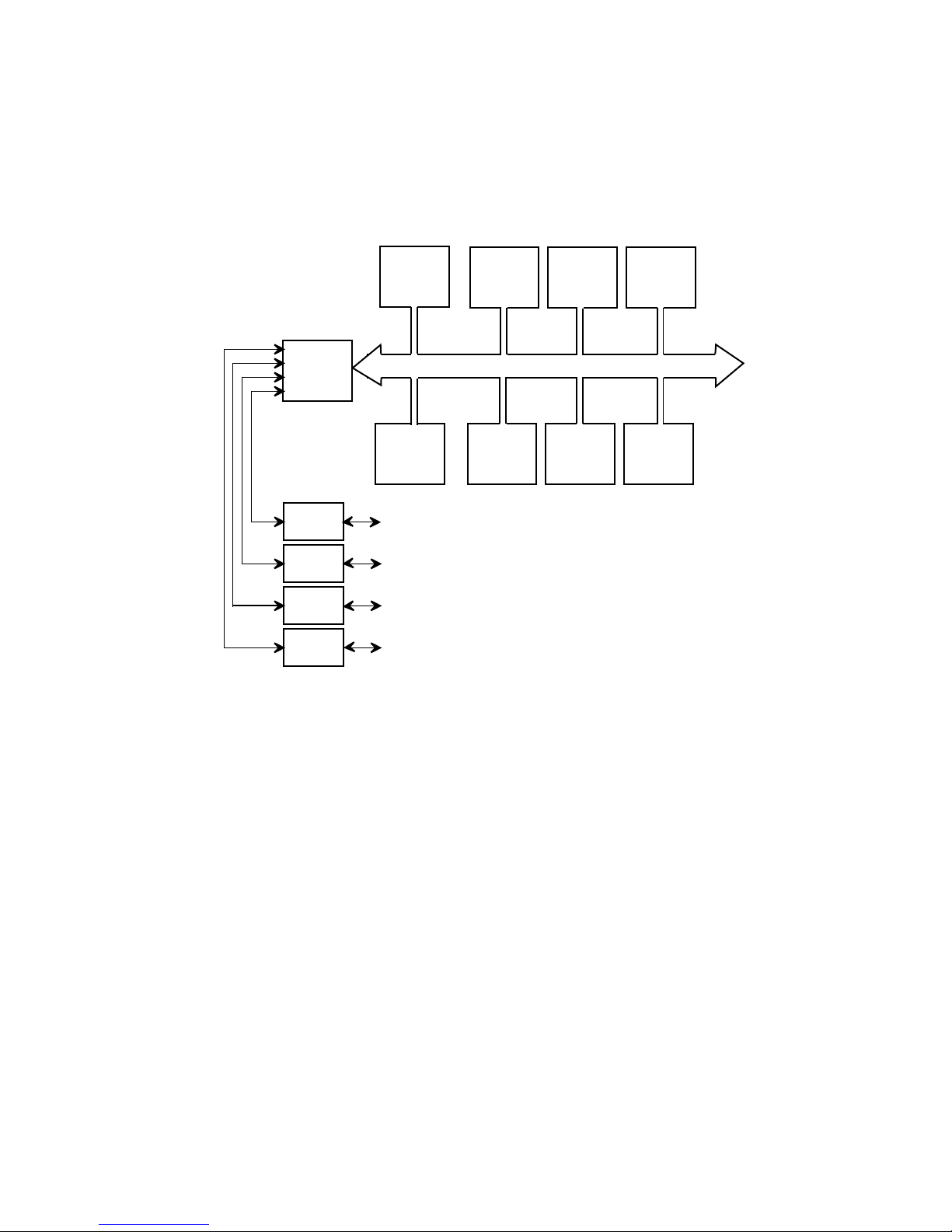
Futurebus+, or PCI bus. The local I/O options on the integrated I/O
port appear to software as a PCI bus connected to a hose.
Figure 1-1 shows a block diagram of the 8400 system.
Figure 1-1 AlphaServer 8400 System Block Diagram
TLSB I/O
Port
Module
XMI
Interface
FBUS+
Interface
XMI
Interface
PCI
Interface
CPU,
MEM, or
I/O Module
TLSB Bus; 40-bit address path, 256-bit data path
CPU or
MEM
Module
To/from XMI
To/from Futurebus+
To/from XMI
To/from PCI
CPU,
MEM, or
I/O Module
CPU or
MEM
Module
CPU,
MEM, or
I/O Module
CPU or
MEM
Module
CPU,
MEM, or
I/O Module
CPU or
MEM
Module
BXB0813.AI
1.2 Bus Architecture
The system bus, the TLSB, is a limited length, nonpended, pipelined synchronous bus with separate 40-bit address and 256-bit data buses. The
TLSB supports a range of cycle times, from 10 to 30 ns. At 10 ns, the
maximum bandwidth available is 2.1 Gbytes/sec.
The TLSB runs synchronously with the CPU clock, and its cycle time is an
integer multiple of the CPU clock. Memory DRAM cycle time is not synchronous with the TLSB clock. This permits memory access times to be
adjusted as the CPU clock is adjusted.
The TLSB supports nine nodes. One node (slot 8) is dedicated to I/O. This
node has special arbitration request lines that permit the node to always
arbitrate as the highest priority or the lowest priority device. This scheme
guarantees the node a maximum upper bound on memory latency. Any of
the other eight nodes can be a CPU or memory node. Four of these remaining nodes can be I/O ports.
Access to the address bus is controlled by a distributed arbitration scheme
implemented by all nodes on the bus. Access to the data bus is governed
by the order in which address bus transactions occur. Address and data
1-2 Overview
Page 23

bus transactions may be overlapped, and these transactions may be overlapped with bus arbitration. Arbitration priority rotates in a round-robin
scheme among the nodes. A node in the slot dedicated to I/O follows a special arbitration algorithm so that it cannot consume more than a certain
fraction of the bus bandwidth.
The TLSB supports a conditional write-update cache protocol. This protocol allows a node to implement a write-back cache while also offering a
very efficient method for sharing writable data. All bus data transfers are
naturally aligned, 64-byte blocks.
With this protocol, a CPU cache retains the only up-to-date copy of data.
When this data is requested, the CPU with the most recent copy returns it.
Memory ignores the transaction. Special TLSB signal lines coordinate this
operation.
The TLSB uses parity protection on the address bus. One parity bit protects the address, and one bit protects the command and other associated
fields.
The data bus is protected by ECC. An 8-bit ECC check code protects each
64 bits of data. The generator and ultimate user of the data calculate ECC
check codes, report, and correct any errors detected. TLSB bus interfaces
check (but do not correct) ECC to aid in error isolation. For example, an
I/O device calculates ECC when DMA data is written to memory. When a
CPU reads this data, the TLSB interface on the CPU module checks and
notes any errors, but the DECchip 21164 actually corrects the data prior to
using it.
The ECC check code corrects single-bit errors. It detects double-bit errors,
and some 4-bit errors, in each 64-bit unit of data.
1.3 CPU Module
The CPU module contains one or two DECchip 21164 microprocessors. In
dual-processor modules, each processor operates independently and has
its own backup cache. A single interface to the TLSB is shared by both
CPU chips. The interface to console support hardware on the CPU module
is also shared by both microprocessors. The main sections of the CPU
module are:
• DECchip 21164
• Backup cache
• TLSB interface
• Console support hardware
A simple block diagram of the CPU module is given in Chapter 3.
1.3.1 DECchip 21164
The DECchip 21164 microprocessor is a CMOS-5 (0.5 micron) superscalar,
superpipelined implementation of the Alpha architecture. A brief listing of
the DECchip 21164 features is given in Chapter 3. DECchip 21164 implements the Alpha architecture together with its associated PALcode. Refer
Overview 1-3
Page 24

to the DECchip 21164 Functional Specification for a complete description
of the DECchip 21164 and PALcode.
1.3.2 Backup Cache
Each backup cache (B-cache) is four Mbytes in size. In a dual-processor
module there are two independent backup caches, one for each CPU. Each
B-cache is physically addressed, direct-mapped with a 64-byte block and
fill size. The B-cache is under the direct control of the DECchip 21164.
The B-cache conforms to the conditional write-update cache coherency protocol as defined in the TurboLaser System Bus Specification.
The CPU module contains a duplicate copy of each B-cache tag store used
to maintain systemwide cache coherency. The module checks the duplicate
tag store on every TLSB transaction and communicates any required
changes in B-cache state to the DECchip 21164.
The CPU module also maintains a victim buffer for each B-cache. When
the DECchip 21164 evicts a cache block from the B-cache, the victim buffer
holds it. The DECchip 21164 writes the block to memory as soon as possible.
1.3.3 TLSB Interface
The CPU module uses six gate arrays to interface to the TLSB. The MMG
gate array orders requests from both DECchip 21164 processors. The ADG
gate array contains the TLSB interface control logic. It handles TLSB arbitration and control, monitors TLSB transactions, and schedules data movements with either processor as necessary to maintain cache coherency.
Four identical DIGA gate arrays interface between the 256-bit TLSB data
bus and the 128-bit DECchip 21164 processors. See Chapter 3 for brief
discussions of the gate arrays.
1.3.4 Console Support Hardware
The CPU module console support hardware consists of:
• Two Mbytes of flash EEPROM used to store console and diagnostics
software. A portion of this EEPROM is used to store module and system parameters and error log information.
• One UART used to communicate with the user and power supplies.
• Battery-powered time-of-year (TOY) clock.
• One green LED to indicate CPU module self-test status.
• A second console UART for each processor, for engineering and manu-
facturing debug use.
An 8-bit Gbus, controlled by the ADG gate array, is provided to access the
console support hardware.
1.4 Memory Module
Memory modules are available in the following sizes: 128 Mbytes, 256
Mbytes, 512 Mbytes, 1 Gbyte, and 2 Gbytes. Sizes up to 1 Gbyte are sup-
1-4 Overview
Page 25

ported by a single motherboard design. The 2-Gbyte memory option uses
a different motherboard and SIMM design.
A maximum of seven memory modules may be configured on the TLSB (in
a system with one CPU module and one I/O module). Thus, the maximum
memory size is 14 Gbytes, using 2-Gbyte modules.
Memory operates within the 10–30 ns TLSB cycle time range. To keep
memory latency low, the memory module supports three different DRAM
cycle times. As TLSB cycle time is decreased (slowed down), the memory
module cycle time can be increased (sped up) to ensure that data latency
remains relatively constant, independent of TLSB cycle time.
Each memory module is organized into two banks of independently accessible random memory. Bank interleaving occurs on 64-byte boundaries,
which is the TLSB data transfer size.
Different size memory modules can be interleaved together. For example,
four 128-Mbyte modules can be combined to appear as a single 512-Mbyte
module, and this set can be interleaved with a 512-Mbyte module. In this
case, the five modules are four-way interleaved.
Memory is protected by a 64-bit ECC algorithm. An 8-bit ECC check code
protects each 64 bits of data. This algorithm allows correction of single-bit
failures and the detection of double-bit and some nibble failures. The same
algorithm is used to protect data across the TLSB and within the CPU
module caches. ECC is checked by the memory when data is read out of
memory. It is also checked when data is received from the TLSB, prior to
writing data into the memory. Memory is designed so that a single failing
DRAM cannot cause an uncorrectable memory error.
The memory module does not correct ECC errors. If a data block containing a single-bit ECC error is written by a CPU or I/O device to memory, the
memory checks the ECC and signals a correctable error, but it does not
correct the data. The data is written to the DRAMs with the bad ECC
code. Only CPU and I/O port modules correct single-bit ECC errors.
Refer to Chapters 4 and 5 for a thorough discussion of the memory module.
1.5 I/O Architecture
The I/O system components consist of:
• I/O port module (KFTHA)
• Integrated I/O port module (KFTIA)
• XMI bus adapter (DWLMA)
• Futurebus+ adapter (DWLAA)
• PCI bus adapter (DWLPA)
• Memory Channel interface (RM in register mnemonics)
The KFTHA and KFTIA modules reside on the TLSB and provide the interface between the TLSB and optional I/O subsystems.
The KFTHA provides connections for up to four optional XMI, Futurebus+,
or PCI buses, in any combination, through a cable called a hose.
The KFTIA provides a connection to one optional XMI, Futurebus+, or PCI
bus through a hose. It also contains an on-module PCI bus with connec-
Overview 1-5
Page 26

tion to two 10BaseT Ethernet ports, one FDDI port, and three FWD and
one single-ended SCSI ports.
The DWLMA is the interface between a hose and a 14-slot XMI bus. It
manages data transfer between XMI adapters and the I/O port.
The DWLAA is the interface between a hose and a 10-slot Futurebus+ card
cage. It manages data transfer between Futurebus+ adapters and the I/O
port.
The DWLPA is the interface between a hose and a 12-slot, 32-bit PCI bus.
It manages data transfer between PCI adapters and the I/O port. The PCI
is physically implemented as three 4-slot PCI buses, but these appear logically to software as one 12-slot PCI bus. The PCI also supports the EISA
bus.
The Memory Channel interface connects a hose to a 100 MB/sec Memory
Channel bus. This bus is a memory-to-memory computer system interconnect, and supports up to 8 nodes. With appropriate fiber optic bridges, this
can be expanded to 64 nodes.
The TLSB supports up to three I/O ports of either type. The first (or only)
I/O port in the system is installed in the dedicated I/O TLSB slot (slot 8).
Any latency-sensitive devices should be configured to this I/O port. The
second I/O port, if present, should be installed in the highest number slot
accommodating an I/O port.
The I/O port uses mailbox operations to access CSR locations on the remote
I/O bus. Mailbox operations are defined in the Alpha System Reference
Manual. For PCI buses, direct-mapped I/O operations are also supported.
1.6 Software
1.6.1 Console
The system software consists of the following components:
• Console
• OpenVMS Alpha operating system
• Digital UNIX operating system
• Diagnostics
The following subsections provide brief overviews of the system software
components.
The console firmware supports the two operating systems as well as the
following system hardware:
• DECchip 21164 processor
• One or two processors per CPU module and up to 12 processors per
system
• Multiple I/O ports per system
• PCI I/O bus and peripherals
• Memory Channel
The console supports boot devices on the following I/O port adapters:
1-6 Overview
Page 27

• KDM70 – XMI to SI disk/tape
• KZMSA – XMI to SCSI disk/tape
• KFMSB – XMI to DSSI disk/tape and OpenVMS clusters
• CIXCD-AC – XMI to CI HSC disk/tape and OpenVMS clusters
• DEMNA – XMI to Ethernet networks and OpenVMS clusters
• DEMFA – XMI to FDDI networks and OpenVMS clusters
• DEFAA – Futurebus+ to FDDI networks and OpenVMS clusters
Booting is suported from PCI SCSI disk, Ethernet, and FDDI devices.
1.6.2 OpenVMS Alpha
OpenVMS Alpha fully supports the system. Symmetrical multiprocessing,
OpenVMS clusters, and all other OpenVMS Alpha features are available
on the system. OpenVMS Alpha is released only on CD-ROM, which is
supported for initial system load through a SCSI device.
1.6.3 Digital UNIX
The system fully supports the Digital UNIX operating system, which is released only on CD-ROM. CD-ROM is supported for initial system load
through a SCSI device.
1.6.4 Diagnostics
The system diagnostic software is composed of:
• ROM-based diagnostics
• The loadable diagnostic execution environment
• Online exercisers
1.6.4.1 ROM-Based Diagnostics
CPU module ROMs contain a complete set of diagnostics for the base system components. These diagnostics include CPU, memory, I/O port, and
generic exercisers for multiprocessing, memory, and disks.
The following diagnostics are included in the CPU module ROMs:
• CPU module self-test
• CPU/memory interaction tests
• Multiprocessor tests
• I/O port tests
• DWLMA tests
• DWLAA tests
• Futurebus+ bus exerciser (FBE) tests
• System kernel and I/O exerciser script
— Floating-point exerciser
Overview 1-7
Page 28

— Cache/memory exerciser
— I/O port/DWLMA loopback exerciser
— Disk/tape device exerciser
— Network exerciser
— FBE exerciser
— XCT (XMI bus exerciser) exerciser
• Manual tests
A subset of these diagnostics is invoked at system power-up. Optionally,
they may be invoked on every system boot. The subset can also be invoked
by the user through console command.
Note that any of the diagnostics listed above can be individually invoked
by the user through console command.
1.6.4.2 Loadable Diagnostic Execution Environment
The loadable diagnostic executive is essentially a loadable version of the
ROM-based diagnostic executive. It supports loading from any device for
which a console boot driver exists. Once loaded, diagnostics are run and
monitored using the same commands as for the ROM-based diagnostics.
The LFU firmware update utility is a loadable program. This utility updates CPU console and diagnostic firmware, and firmware on I/O adapters.
1.6.4.3 Online Exercisers
The VET online exerciser tool is available for the systems. This tool provides a unified exercising environment for the operating systems. This exerciser is on each operating system kit. It is invoked as a user-mode program.
The following VET exercisers are available:
• Load
• File
• Raw disk
• Tape
• Memory
• Network
1-8 Overview
Page 29

2.1 Overview
Chapter 2
TLSB Bus
This chapter provides a brief overview of the TLSB bus. For more detailed
discussions and timing diagrams for the various bus cycles, refer to the
TurboLaser System Bus Specification.
The TLSB bus is a limited length, nonpended, synchronous bus with a
separate address and data path. Ownership of the address bus is determined using a distributed arbitration protocol. The data bus does not require an arbitration scheme. The data bus transfers data in the sequence
order in which command/addresses occur. The combination of separate address and data paths with an aggressive arbitration scheme permits a low
latency protocol to be implemented.
Because the address and data buses are separate, there is maximum overlap between command issues and data return. The TLSB also assumes
that the CPU nodes run the module internal clock synchronous to the bus
clock, eliminating synchronizers in the bus interface and their associated
latency penalties. The TLSB provides control signals to permit nodes to
control address and data flow and minimize buffering.
The TLSB operates over a range of 10 to 30 ns clock cycles. This corresponds to a maximum bandwidth of 2.1 Gbytes/sec and a projected minimum latency of 170 ns with a 10 ns clock cycle. Memory latency is reduced
by improving the DRAM access time. Because the address bus and data
bus are separate entities, the slot for passing data on the data bus is variable and directly affected by the DRAM access time. Therefore, any decrease in DRAM access time is reflected in a decrease in memory latency.
The AlphaServer 8400 has nine physical nodes on the TLSB centerplane,
numbered 0–8. CPU and memory modules are restricted to nodes 0–7. I/O
ports are restricted to nodes 4–8. These five nodes are on the back side of
the centerplane. AlphaServer 8200 supports the five backplane nodes
only. I/O modules are restricted to nodes 6, 7, and 8. Node 8 in both models is dedicated to the I/O module and has the special property of both high
and low priority arbitration request lines that are used to guarantee that
memory latency is no worse than 1.7 µs. An I/O port in any other node
uses the standard arbitration scheme, and no maximum latency is specified.
TLSB Bus 2-1
Page 30

2.1.1 Transactions
2.1.2 Arbitration
A transaction couples a commander node that issues the request and a
slave node that sequences the data bus to transfer data. This rule applies
to all transactions except CSR broadcast space writes. In these transactions, the commander is responsible for sequencing the data bus. CPUs
and I/O nodes are always the commander on memory transactions and can
be either the commander or the slave on CSR transactions. Memory nodes
are slaves in all transactions.
Address bus transactions take place in sequence as determined by the winner of the address bus arbitration. Data bus transactions take place in the
sequence in which the commands appear on the address bus. All nodes internally tag the command with a four-bit sequence number. The number
increments as each command is acknowledged. To return data, the slave
node sequences the bus to start the transfer.
The address bus protocol allows aggressive arbitration where devices can
speculatively arbitrate for the bus and where the winner can no-op out the
command if the bus is not needed. The bus provides eight request lines for
the nodes that permit normal arbitration. Node 8 has high and low arbitration request lines that permit an I/O port to limit maximum read latency.
2.1.3 Cache Coherency Protocol
The TLSB supports a conditional write-update protocol that permits the
use of a write-back cache policy, while providing efficient handling of
shared data across the caches within the system.
2.1.4 Error Handling
The TLSB implements error detection and, where possible, error correction. Transaction retry is permitted as an implementation-specific option.
Four classes of errors are handled:
• Soft errors, hardware corrected, transparent to software (for example,
single-bit ECC errors).
• Soft errors requiring PALcode/software support to correct (for example,
cache tag parity errors, which can be recovered by PALcode copying
the duplicate tag to the main tag).
• Hard errors restricted to the failing transaction (for example, a doublebit error in a memory location in a user’s process. This would result in
the process being aborted and the page being marked as bad). The system can continue operation.
• System fatal hard errors. The system integrity has been compromised
and continued system operation cannot be guaranteed (for example,
bus sequence error). All outstanding transactions are aborted, and the
state of the system is unknown. When a system fatal error occurs, the
bus attempts to reset to a known state to permit machine check handling to save the system state.
2-2 TLSB Bus
Page 31

The TLSB implements parity checking on all address and command fields
on the address bus, ECC protection on the data field, and protocol sequence checking on the control signals across both buses.
2.1.5 TLSB Signal List
Table 2-1 lists the signals on the TLSB. Signal name, function, and default state are given. After initialization, the bus drives the default value
when idle.
Table 2-1 TLSB Bus Signals
Signal Name
TLSB_D<255:0>
TLSB_ECC<31:0>
TLSB_DATA_VALID<3:0>
TLSB_ADR<39:3>
TLSB_ADR_PAR
TLSB_CMD<2:0>
TLSB_CMD_PAR
TLSB_BANK_NUM<3:0>
TLSB_REQ8_HIGH
TLSB_REQ8_LOW
TLSB_REQ<7:0>
TLSB_HOLD
TLSB_DATA_ERROR
TLSB_FAULT
TLSB_SHARED
TLSB_DIRTY
TLSB_STATCHK
TLSB_CMD_ACK
TLSB_ARB_SUP
TLSB_SEND_DATA
TLSB_SEQ<3:0>
TLSB_BANK_AVL<15:0>
TLSB_LOCKOUT
TLSB_PH0
TLSB_NID<2:0>
TLSB_RSVD_NID<3>
TLSB_RESET
CCL_RESET L
TLSB_BAD L
TLSB_LOC_RX L
TLSB_LOC_TX L
TLSB_PS_RX L
Default
State Function
L
L
L
L
L
L
L
L
L
L
L
L
L
L
L
L
L
L
L
L
L
L
L
L
H
H
H
H
H
256-bit wide data bus
Quadword ECC protection bits
Data valid masks
Physical memory address
Address parity
Command field
Command and bank number parity
Encoded bank number
Slot 8 high priority bus request
Slot 8 low priority bus request
Normal bus requests
Data bus stall
Data bus error detected
Bus fault detected
Cache block is shared
Cache block is dirty
Check bit for shared and dirty
Command acknowledge
Arbitration disable
Send data
Sequence number
Bank available lines
Lockout
Clock
Node identification
Spare node identification
Bus reset
CCL reset
Self-test not successful
Local console receive data
Local console transmit data
Power supply receive status
TLSB Bus 2-3
Page 32

Table 2-1 TLSB Bus Signals (Continued)
Default
Signal Name
State Function
TLSB_PS_TX L
TLSB_EXP_SEL<1:0> L
TLSB_SECURE L
LDC_PWR_OK L
PIU_A_OK L
PIU_B_OK L
TLSB_RUN L
TLSB_CON_WIN L
ON_CMD
SEQ_DCOK
TLSB_DCOK L
EXT_VM_ENB
VM3
VM5
V3_OUT
V5_OUT
GB2CCLSPA
MFG_MODE L
SER_NUM_CLK
SER_NUM_DAT
H
H
L
L
L
L
H
H
L
Power supply transmit status
Expander select
Secure console
Local disk converter
I/O unit A power OK
I/O unit B power OK
System run indicator
Console win status
DC-DC converter power on enable
Module power OK
Driver output enable
Voltage margin control
Voltage margin control
Voltage margin control
Voltage margin control
Voltage margin control
CCL spare
Manufacturing test
Serial number access
Serial number access
2-4 TLSB Bus
Page 33

2.2 Operation
This section offers an overview of the TLSB bus operations. Topics include:
• Physical node identification
• Virtual node identification
• Address bus concepts
• Address bus arbitration
• Address bus cycles
• Address bus commands
• Data bus concepts
• Data bus functions
• Miscellaneous bus signals
The reader is referred to the engineering specification for more detail on
the topics covered in this chapter.
2.2.1 Physical Node ID
The AlphaServer 8400 features nine nodes (corresponding to the nine
physical connectors) on the TLSB. Each CPU, memory, or I/O port module
receives signals TLSB_NID<2:0> to identify its node number. The
TLSB_NID<2:0> signals are selectively grounded and are pulled up on the
module. Node 0 and node 8 receive TLSB_NID<2:0> equal to zero. Since
an I/O port module is not permitted in node 0 and is the only module type
permitted in node 8, an I/O adapter that receives TLSB_NID<2:0> equal to
zero knows it is in node 8. Table 2-2 identifies the nodes on the TLSB.
The AlphaServer 8200 has nodes 4 to 8 only. Node 4 must be a CPU module. Node 8 is dedicated to an I/O module.
Table 2-2 TLSB Physical Node Identification
Node/Slot
TLSB_NID<2:0>
000
001
010
011
100
101
110
111
000
Number Description
0
1
2
3
4
5
6
7
8
CPU or memory module
CPU or memory module
CPU or memory module
CPU or memory module
CPU, memory or I/O module
CPU, memory, or I/O module
CPU, memory, or I/O module
CPU, memory, or I/O module
I/O module
TLSB Bus 2-5
Page 34

2.2.2 Virtual Node Identification
TLSB system operation requires that certain functional units can be identified uniquely, independent of their physical location. Specifically, individual memory banks and CPUs must be uniquely addressable entities at the
system level. As multiple memory banks and CPUs are implemented on
single modules, a physical node ID is insufficient to uniquely address each
bank or each CPU. The AlphaServer 8400/8200 systems, therefore, employ
virtual node IDs, software-generated, dynamically stored IDs, to identify
its functional units. Note that CSR addresses are still managed on a node
basis within the system and are keyed off the physical node ID.
Virtual node IDs are set by writing the TLVID register fields with the
value required. The console is responsible for initializing the values at
power-up. A module can have multiple virtual node IDs associated with it;
for example, dual CPUs or memory controllers with multiple memory
banks. The maximum number of virtual IDs per TLSB module is eight.
The unused ID fields are not implemented, and a CSR read must return 0
in the unused fields. Virtual node IDs are identified by the type of module
they reside on. They are:
• CPUID, range 0–15
• MEMID, range 0–15. This corresponds to the memory bank number
MEM_BANKn (n = 0 to 15).
2.2.3 Address Bus Concepts
The TLSB implements separate address and data buses. The purpose of
the address bus is to signal a bus node (usually memory) with an address
so that it can transfer data as soon as possible. The TLSB uses the memory bank to control flow of addresses on the bus. Once a bank has been
addressed and it is busy, no other commander can use that bank until it
becomes free. An analysis of memory latency showed that the following
actions in the address propagation path directly contribute to latency:
• Cache tag lookup and compare
• Check for bank busy
• Bus arbitration
• Address bank decode in the memory
The TLSB attempts to address these issues to create a low latency system.
All memory is divided into banks. A bank is addressed by a unique 4-bit
bank number transmitted on the TLSB address bus. The CPU always has
to perform a bank decode to decide if it can issue the request. Therefore,
the CPU transmits the bank number along with the address and command
on the address bus. A compare of the bank’s virtual ID to the transmitted
bank number is performed in the memory bank controller. This simplifies
the memory address decoding and permits fast memory addressing.
On a TLSB CPU module a tag lookup and compare is permitted to take
place in parallel with bus arbitration. When the CPU performs a tag
probe, it passes a valid signal to the CPU memory interface to indicate
that the current address is being used in a cache lookup. This valid signal
can be used to initiate a bus request and gain early access to the address
bus. This means that a cache tag lookup that hits in the cache can potentially perform a request and win the bus. By the time the CPU has to
2-6 TLSB Bus
Page 35

drive the address and command, the outcome of the tag lookup can be
evaluated by the bus interface. If the lookup is a hit, then the CPU bus
interface nulls the TLSB command field and cancels the request. Although
this consumes potentially needed address bus slots, the address bus requires two cycles to initiate a command and the data bus requires three cycles per transaction. This means that there are surplus address bus slots
beyond the number required to keep the data bus busy. Therefore, the
penalty of a false arbitration on data bus bandwidth is minimized. The
pipelined nature of the bus means that there are potential bank conflicts
that can only be resolved by nulling the address command. The bank decode can also be hidden under the request and arbitration cycles.
Bus arbitration by the CPU under these aggressive conditions is called
"early arbitration." When the request has to be nulled due to bank conflict
or a cache hit, it is called "false arbitration."
All address bus commands (except nulled commands) require acknowledgment two cycles after the issue of the bank address on the bus, or no data
is transferred. This mechanism permits the commander node to determine
if a slave node will respond. On a normal transaction when a commander
issues a request, the sequencing of the data bus is the responsibility of the
slave node. All nodes must look for the acknowledgment; only acknowledged commands sequence the data bus.
The address bus permits flow control by use of the signal TLSB_ARB_SUP.
This signal permits commander nodes to stop address bus arbitration, thus
preventing further addresses from propagating to the bus.
All TLSB memory transactions take place on a cache block boundary (64
bytes). Memory is accessed with signals TLSB_ADR<39:5> on the address
bus. TLSB_ADR<39:6> addresses one block. TLSB_ADR<5> specifies the
first 32-byte subblock to be returned (wrapped). Use of TLSB_ADR<4:3>
is implementation specific. Figure 2-1 shows mapping of physical addresses to the address bus.
Figure 2-1 TLSB Memory Address Bit Mapping
39
Processor Byte Address
64-Byte Block Address
39
Two special address bus commands permit an I/O device to perform atomic
transactions on sizes under 64 bytes. The first command permits a 64-byte
read to put a special lock on a bank, and the second command permits the
subsequent write to unlock the bank. Because a busy bank cannot be accessed by another node, this command pair guarantees atomic access to
the cache block that needs to be modified.
6
56
Wrap
5
4
0
Address
Bus
Field
BXB0828.AI
TLSB Bus 2-7
Page 36

2.2.3.1 Memory Bank Addressing Scheme
The TLSB supports one terabyte of physical memory. The memory address space is accessed by a 40-bit byte address. The granularity of accesses on the TLSB is a 64-byte cache block. I/O adapters that need to manipulate data on boundaries less than 64 bytes require the commander
node to perform an atomic Read-Modify-Write transaction.
Physical memory on the TLSB is broken into banks. The commander decodes the 40-bit physical address into a memory bank number. TLSB supports a maximum of 16 memory banks in the system. Each commander
node contains eight memory mapping registers. Each mapping register
can decode two bank numbers.
A memory module can have multiple physical banks. Each bank is assigned a virtual bank number. The bank number is written in the TLVID
register. This register contains support for up to eight virtual IDs. For a
memory module these fields are named virtual bank numbers
MEM_BANKn, where n is in the range 0–15. This scheme, combined with
the address decoding scheme, permits flexible memory interleaving. When
an address is transmitted on the TLSB, the bank controllers on memory
nodes only need to perform a four-bit compare with the virtual ID to determine if the bank is being addressed. This decode is much quicker than a
full address decode. The address is propagated before the DRAM bank is
determined and RAS is asserted to the proper bank.
2.2.3.2 CSR Addressing Scheme
CSRs are accessed using two special command codes on the address bus.
Both local and remote CSRs can be accessed. Local CSRs exist on TLSB
nodes and can be directly accessed through the physical node ID. Remote
CSRs exist on I/O devices connected to I/O buses on I/O adapter nodes, and
must be accessed through the I/O node using its physical node ID. CSR
write commands can also be broadcast to all TLSB nodes in a single bus
transaction.
CSRs are accessed by the 37-bit address on the address bus. CSR accesses
to nonexistent nodes are not acknowledged. CSR accesses to a node that is
present in the system are always acknowledged on the address bus even if
the CSR does not exist. The node that acknowledges the address is responsible for sequencing the data bus where 64 bytes of data are transferred. If
a read is performed to a valid node, but to a CSR that is not implemented,
the return data is Unpredictable.
CSR write commands addressing broadcast space are acknowledged by the
commander. If the commander acknowledges the command, it also sequences the data bus and transmits data. All receiving nodes optionally
implement the write command. If the CSR does not exist, then the broadcast write is ignored. Receiving nodes may take action based on the broadcast space address even if the command is not acknowledged, if no data is
needed (for example, a decrement counter operation). A read in broadcast
space is illegal, and the commander should not issue such a command. If a
broadcast space CSR read is detected on the bus, all nodes ignore the command.
2-8 TLSB Bus
Page 37

2.2.3.3 Memory Bank Address Decoding
The minimum bank size for the TLSB address decode scheme is 64
Mbytes.
To address memory, a CPU or I/O node must perform a memory bank decode to test the status of the bank. The memory modules transmit the
status of each bank on the 16 TLSB_BANK_AVL lines. This permits a
node to sense the state of the bank from the bus. The TLSB early arbitration scheme allows a node to request the bus before the bank decode takes
place. If the bank is busy, or the previous address bus command made the
bank busy, the command will be nulled if the address bus is granted. If
the requester does not win the arbitration, the request is dropped. On the
TLSB the CPU or I/O node must decode the bank address prior to issuing
the command.
Each address bus commander (CPU or I/O) must implement the eight
memory mapping registers named TLMMRn, where n is in the range 0–7.
Each register decodes the bank number n, and may optionally decode the
bank number n+8. A total of 16 bank numbers can be decoded using these
eight registers. The bank decode registers are loaded by the console at
power-up after the memory configuration has been determined. See Chapter 7 for the description of the TLMMRn registers.
Since each memory module contains two banks, a single TLMMRn register
can be used for decoding bank numbers. Table 2-3 shows the values for
SBANK, INTMASK, and INTLV fields of the TLMMRn register.
Table 2-3 Interleave Field Values for Two-Bank Memory Modules
Interleave
Level
2-way
4-way
8-way
16-way
Number of
Modules
Interleaved
1
2
4
8
Figure 2-2 shows the address decode process.
TLMMRn
<SBANK>
0
0
0
0
TLMMRn
<INTMASK>
0
1
2
3
TLMMRn
<INTLV> Bank n Bank n+8
Not applicable
<0:1>
<0:3>
<0:7>
ADR<6>=0
ADR<7>=0
ADR<8>=0
ADR<9>=0
ADR<6>=1
ADR<7>=1
ADR<8>=1
ADR<9>=1
TLSB Bus 2-9
Page 38

Figure 2-2 Address Decode
39 26 25
Physical Address ADRMASK ADDRESS
Decode and Mask
Compare
861
0
10 8
Address Hit
PHAdr INTMASK INTLV
Mask
Mask
Compare
Valid
Interleave Hit
AND
12
Decode and Mask
Bank Hit
BXB0830.AI
When a physical address is presented to the bank decode logic, all valid address bits, as determined by the ADRMASK field, are compared with their
corresponding physical address bits. A match between all address bits and
their corresponding physical address bits indicates an address space hit.
All valid interleave bits, as determined by the INTMASK field, are compared with their corresponding physical address bits. A match between all
INTLV bits and their corresponding physical address bits indicates an interleave hit. If the compares of both address space and interleave result in
hits, and the Valid bit is set, then the bank associated with this register is
being addressed. The resulting bank hit signal is encoded into a 4-bit
TLSB bank number from the register number, or register number + 8.
For every physical memory bank, a memory bank number is set by the
console in the corresponding virtual node ID field in a node’s Virtual ID
register (TLVID). The console sets up the corresponding memory mapping
register TLMMRn in the commander nodes. If a bank number is generated for which no virtual memory ID exists, the operation will never complete.
NOTE: If two TLMMRn registers generate a bank hit while decoding an address,
the resulting bank number is Unpredictable. This is the result of improperly initialized registers and is considered a software error. Unexpected or
inconsistent behavior may result.
2-10 TLSB Bus
Page 39

2.2.3.4 Bank Available Status
TLSB_BANK_AVL indicates that a bank is available for use. When not
asserted, no requests except Write Bank Unlock can be issued to that
bank.
Each memory bank has one of the TLSB_BANK_AVL<15:0> signals assigned to it by the console. The number of the TLSB_BANK_AVL bit corresponds to the bank number assigned to that bank. TLSB_BANK_AVL is
deasserted two cycles after the command is driven on the bus, and is asserted four cycles before the bank is available to accept new commands.
The earliest the TLSB_BANK_AVL bit can be asserted is two cycles following the time when the shared and dirty status is available on the bus (that
is, TLSB_HOLD is deasserted). This is required so that CPUs have time
to update the tag status of the block before another command can be targeted at that block.
I/O devices can use bus commands Read Bank Lock and Write Bank Unlock to guarantee atomic Read-Modify-Write access to a block. The
TLSB_BANK_AVL bit is deasserted in response to a Read Bank Lock and
remains deasserted until a Write Bank Unlock is issued. An I/O device can
arbitrate for a busy bank, but only when the bank is busy because of a
Read Bank Lock that it issued. The I/O device must control the sequence
as follows:
• Read Bank Lock must be followed by a Write Bank Unlock as the next
operation to that bank.
• The earliest the I/O device can request the bus for the Write Bank Unlock command is two cycles following the time when the shared and
dirty status for the Read Bank Lock command is available on the bus
(that is, TLSB_HOLD is deasserted).
• The Write Bank Unlock must be issued as soon as possible after the
data from the Read Bank Lock command is received.
• Intervening commands to other banks may be issued.
2.2.3.5 Address Bus Sequencing
For the data bus to return data in order, each valid bus command must be
tagged in the slave and commander TLSB interface with a sequence number. A maximum of 16 outstanding transactions are allowed on the bus at
any one time. This requires a wrapping 4-bit count. The first command following a reset sequence must be tagged with a sequence number of zero.
When a command is acknowledged, the sequence number is held by the
slave and commander. When the data bus sequence counter matches the
tagged sequence, the data transfer takes place.
All nodes increment their address bus sequence counters on the receipt of
a command acknowledge. When a command is nulled (for example, due to
false arbitration or bank conflict), the sequence number is not incremented.
All nodes watch the data bus sequence. If a transaction is lost or incorrectly sequenced, the TLSB node interfaces will detect an illegal sequence.
Sequence errors are regarded as system fatal.
TLSB Bus 2-11
Page 40

2.2.4 Address Bus Arbitration
The TLSB bus has demultiplexed address and data buses. These buses operate independently and are related only in as much as a valid command
on the address bus will result in a data transfer on the data bus at some
later time.
2.2.4.1 Initiating Transactions
To initiate a bus transaction, a module must request the bus and arbitrate
for access to the bus with other requesting modules. Only when it wins arbitration can a device drive the command, address, and memory bank
number onto the bus. Only CPUs and I/O modules can initiate transactions.
2.2.4.2 Distributed Arbitration
The TLSB uses a distributed arbitration scheme. Ten request lines
TLSB_REQ8_HIGH, TLSB_REQ8_LOW, and TLSB_REQ<7:0> are driven
by the CPU or I/O modules that wish to use the bus. All modules independently monitor the request lines to determine whether a transaction
has been requested, and if so, which module wins the right to send a command cycle. Request lines are assigned to each node. Nodes 7–0 are assigned TLSB_REQ<7:0>, respectively. Node 8, the dedicated I/O port
node, is assigned TLSB_REQ8_HIGH and TLSB_REQ8_LOW. At powerup, or following a reset sequence, the relative priority of each of the request lines TLSB_REQ<7:0> is initialized to the device’s node ID. Node 7
has the highest relative priority and node 0 the lowest.
2.2.4.3 Address Bus Transactions
CPU and I/O modules can only perform transfers to or from memory banks
that are not currently in use, plus one transfer to or from a CSR. The
maximum number of memory banks in a system is 16. Consequently, the
maximum number of outstanding transactions possible on the bus at one
time is 17. However, due to the size of the sequence number tagged to
each transaction, a limit of 16 outstanding transactions must be enforced.
All CPU and I/O modules are required to assert TLSB_ARB_SUP to prevent arbitration for a 17th command. Individual modules may limit the
number of transactions on the bus to a lower number.
2.2.4.4 Module Transactions
There is no limit to the number of transactions that can be issued by one
module as long as each of the transactions meets the requirements of targeting a nonbusy bank and of requesting the bus separately for each transaction.
2.2.4.5 Address Bus Priority
Each commander node keeps track of the relative priorities of the request
lines TLSB_REQ<7:0>. When a device wins the bus and issues a data
transfer command, it becomes the lowest priority device. Any device whose
priority is below that of the winning device has its priority incremented.
2-12 TLSB Bus
Page 41

Consequently, the priority of any device will eventually bubble up to the
highest level. The no-op command is the only non-data transfer command;
it does not affect priorities.
TLSB_REQ8_HIGH and TLSB_REQ8_LOW are assigned to the I/O module in node 8. These lines represent the highest and the lowest arbitration
priorities. The I/O port uses the high-priority line to guarantee a worstcase latency. I/O ports residing in any node other than node 8 do not have
a guaranteed latency and arbitrate in the same manner as CPU modules,
using the request line assigned to that node.
2.2.4.6 Address Bus Request
A module may request the bus during any cycle. The mechanism for
granting the bus is pipelined. The request cycle is followed by an arbitration cycle and then by a cycle where the command, address, and bank
number are driven on the bus. A new command and address can be driven
in every second cycle.
Idle, request, and arbitration cycles differ as follows. An idle cycle is one
in which no request line is asserted and no arbitration is taking place. A
request cycle is the first one in which a request is asserted, and every second bus cycle after that in which a request is asserted until the bus returns to an idle state. An arbitration cycle is defined as the cycle following
a request cycle.
A device requests the bus by asserting its request line. In the next cycle
all devices arbitrate to see which wins the bus. The winner drives its command type, address, and bank number onto the bus and deasserts the request. The targeted memory module responds by asserting TLSB_CMD_
ACK and by deasserting the TLSB_BANK_AVL line for the targeted bank.
When a module wins arbitration for the bus, whether for real arbitration
or as a result of a false arbitration, it deasserts its request line in the following cycle even if the module has another outstanding transaction.
2.2.4.7 Asserting Request
On a busy bus, every second cycle is considered a request cycle. Request
lines asserted in nonrequest cycles are not considered until the next request cycle (one bus cycle later). Request lines asserted in nonrequest cycles do not get any priority over lines asserted in the request cycle.
When more than one device requests the bus simultaneously, the device
with the highest priority wins the bus. Note that a new address can be
driven only once every two bus cycles.
2.2.4.8 Early Arbitration
CPU modules on the TLSB are allowed to arbitrate for the bus in anticipation of requiring it. This mechanism is referred to as "early arbitration"
and is used to minimize memory latency. The bus protocol provides a
mechanism for a CPU to request the bus, win it, and subsequently issue a
no-op command. This mechanism is referred to as "false arbitration."
A device that implements early arbitration can assert its request line before it requires the bus. If it happens that the bus is not required, the device can deassert its request line at any time. If a request line is asserted
TLSB Bus 2-13
Page 42

in a request cycle, that CPU must take part in the following arbitration cycle even if the bus is no longer required. If the device wins the bus, it asserts a no-op on the bus command lines.
I/O devices in the dedicated I/O port node cannot use early arbitration.
2.2.4.9 False Arbitration Effect on Priority
Relative bus priorities are only updated when a data transfer command is
asserted on the bus. If a device false arbitrates and drives a no-op on the
bus, the bus priorities are not updated.
2.2.4.10 Look-Back-Two
To avoid the possibility of a low-priority device being held off the bus by
high-priority devices false arbitrating, a mechanism is provided that assigns a higher priority to requests that have been continuously asserted for
more than two cycles. This is referred to as the "look-back-two" mechanism.
A request line continuously asserted for more than two cycles must be a
real request (that is, not early, not false). Since bank decode and cache
miss are resolved after two cycles, real requests must be serviced before
newer, potentially false requests. When one or more requests have been
asserted continuously for more than two cycles, these requests have
higher priority than newer requests, and the arbiters consider only requests falling into that category. If the new requests are kept asserted for
longer than two cycles, they are included in the arbitration. The effects of
early arbitration, therefore, are noticed only on buses that are not continuously busy. Busy buses tend to have a queue of outstanding requests waiting to get the bus granted. Requests due to early arbitration are at a lower
priority and are not granted the bus.
If two devices request the bus at the same time, the higher priority device
wins the bus. If the losing device keeps its request line asserted, this is
understood to be a real request, and the device is assigned a higher priority than any newer (potentially false) requests. Note that only a device
continuously asserting its request line for more than two bus cycles is
treated in this manner. Devices must deassert their request line for at
least one cycle between consecutive requests.
NOTE: The I/O port request line TLSB_REQ8_HIGH always has the highest prior-
ity, even in the look-back-two situation.
2.2.4.11 Bank Available Transition
A device can only arbitrate for a bank that is not currently in use. The
TLSB_BANK_AVL<15:0> signals are used to indicate the busy state of the
16 memory banks. TLSB_BANK_AVL lines will be assigned in the memory by the virtual ID loaded by console software at power-up or after system reset. When a bank becomes free, the TLSB_BANK_AVL line associated with it is asserted. There is a window of time after the command is
asserted on the bus before the memory can respond by deasserting the
TLSB_BANK_AVL signal. Consequently, devices must monitor the bus to
determine when a bank becomes busy.
2-14 TLSB Bus
Page 43

CPUs can request the bus without first checking that the bank is busy. If
the bank does turn out to be busy, this is considered a false arbitration,
and the command is a no-op. The device can request the bus again when
the bank is free. To prevent lockout of devices that might have been waiting for the bank, CPUs early arbitrating for the bus cannot issue the command if they request in the cycle when <TLSB_BANK_AVL> asserts on
the bus, or in the subsequent cycle. If a CPU requests a bank before
<TLSB_BANK_AVL> is asserted, it drives a no-op.
2.2.4.12 Bank Collision
If two CPUs request the bus for access to the same bank, the higher priority device is granted the bus and drives the command, address, and bank
number. The lower priority device deasserts its request when it receives
the command and bank number. But if the request cannot be withdrawn
before it gets granted the bus, it must drive a no-op and request again
when the bank becomes free. This conflict is referred to as "bank collision."
Relative bus priorities are only updated when a valid data transfer command is asserted on the bus. If a bank collision occurs, the bus priorities
are not updated as a result of the no-op cycle.
2.2.4.13 Bank Lock and Unlock
I/O ports must merge I/O data into full memory blocks. Commands are
provided on the bus to allow the I/O port to read the block from memory,
merge the I/O data, and write the block back to memory as an atomic
transaction. These commands are the Read Bank Lock and Write Bank
Unlock. In response to a Read Bank Lock, memory deasserts
TLSB_BANK_AVL for that bank and keeps it deasserted until the I/O port
issues a Write Bank Unlock. This effectively denies any other device access to the same block as the bank appears busy.
2.2.4.14 CSR Bank Contention
Nodes arbitrate for CSR accesses in the same manner as they do for memory accesses. CSR accesses must follow the rules relating to early arbitration and look-back-two.
The TLSB protocol allows only one CSR access at a time. There is no explicit CSR bank busy line. Modules must monitor all transactions on the
bus to set an internal CSR busy status and check sequence numbers on return data to clear the CSR busy status. The duration of a CSR access is
from the assertion of the command on the bus to initiate the transaction
until two cycles following the time when the shared and dirty status is
available on the bus (that is, TLSB_HOLD is deasserted). A new request
can be asserted one cycle later. If the command is not acknowledged, the
CSR access ends two cycles after TLSB_CMD_ACK should have appeared
on the bus. A new request can be asserted one cycle later.
If two devices arbitrate for the bus for CSR accesses, the winner drives the
bus. If the second device cannot deassert its request line in time and wins
the bus, it drives a no-op and requests the bus again at a later time.
In the case of a write, a module may be busy writing the data into its CSR
registers after the data transaction on the bus. If this module is involved
TLSB Bus 2-15
Page 44

in subsequent CSR accesses, and it is not ready to source or accept data, it
can delay asserting TLSB_SEND_DATA, or it can assert TLSB_HOLD on
the bus.
2.2.4.15 Command Acknowledge
When a device asserts an address, bank number, and a valid data transfer
command on the bus, the targeted device responds two cycles later by asserting TLSB_CMD_ACK. This indicates that the command has been received and that the targeted address is valid. In the case of CSR broadcast
space writes, where there may be multiple targeted devices, the bus commander asserts TLSB_CMD_ACK.
If an acknowledge is not received, the data bus is not cycled for this command (that is, treated as a no-op). Two cases exist where no acknowledge
is not an error condition: (1) An I/O port does not respond to a CSR access
to a mailbox pointer register. This indicates that the mailbox pointer register is full and that the access should be retried later; (2) A broadcast
space register write, where the act of writing an address is meaningful, but
no data needs to be transmitted.
2.2.4.16 Arbitration Suppress
The commander module asserts TLSB_ARB_SUP to limit the number of
outstanding transactions on the bus to 16. This signal must be asserted in
the cycle following an arbitration cycle, that is in the cycle in which a command, address, and bank number are driven. TLSB_ARB_SUP is asserted
for one cycle, then deasserted for one cycle. This two-cycle sequence is repeated until arbitration can be permitted again. Multiple nodes may assert TLSB_ARB_SUP the first time and the same or fewer nodes may assert it every two cycles thereafter until finally it is not asserted. The cycle
in which it is not asserted is the next request cycle if any device request
signals are asserted at that time; otherwise it is an idle cycle.
Nodes must disregard the value of TLSB_ARB_SUP received during the
second of each two-cycle sequence, as it is Unpredictable. An assertion of
TLSB_ARB_SUP should be converted internally to look like a two-cycle assertion and ignore the value received in the second cycle. This entire sequence repeats every two cycles until it is received deasserted.
Modules may assert requests while TLSB_ARB_SUP is asserted, but no
arbitration is allowed. Priority of devices does not change while
TLSB_ARB_SUP is inhibiting arbitration cycles. Arbitration, when it resumes, follows the normal rules for priority levels and look-back-two.
TLSB_ARB_SUP may also be asserted in response to TLSB_FAULT.
2.2.5 Address Bus Cycles
A TLSB address bus cycle is the time occupied by two cycles of the TLSB
clocks. During the first clock cycle the address, bank, and command bus
signals are driven by the commanding node. The second clock cycle is used
for a dead cycle. This leads to a simpler electrical interface design and the
lowest achievable clock cycle time. There are two types of legal address
bus cycles:
• Data transfer command cycles
2-16 TLSB Bus
Page 45

• No-op command cycles
Two signals are used to provide parity protection on the address bus during all command cycles. TLSB_CMD_PAR is asserted to generate odd parity for the signals TLSB_CMD<2:0>, TLSB_BANK_NUM<3:0>,
TLSB_ADR<39:31>, and TLSB_ADR<4:3>. TLSB_ADR_PAR is asserted
to generate odd parity for the signals TLSB_ADR<30:5>.
When not in use, idle address bus cycles have a predictable value, called
the default bus value. The default value is given in Table 2-1.
2.2.6 Address Bus Commands
Table 2-4 lists the commands used by the TLSB.
Table 2-4 TLSB Address Bus Commands
TLSB_CMD
<2:0> Command Description
000
001
010
011
100
101
110
111
No-op
Victim
Read
Write
Read Bank Lock
Write Bank Unlock
CSR Read
CSR Write
Nulled command
Victim eviction
Memory read
Memory write, or write update
Read memory bank, lock
Write memory bank, unlock
Read CSR data
Write CSR data
No-op
The device that won arbitration has decided to null the command. No action is taken. Priority is not updated. The command is not acknowledged,
and the bus sequence number is not incremented. TLSB_ADR<39:5> and
TLSB_BANK_NUM<3:0> are not used and their contents are Unpredictable.
Victim
Write the block specified by the address and bank number into memory
only. Nonmemory devices do not need to do coherency checks.
Read
Read the block specified by the address and bank number and return that
data over the bus.
Write
Write the block specified by the address and the bank number. Any CPU
containing that block can take an update or an invalidate based on that
CPU’s update protocol.
Read Bank Lock
Used by an I/O port to do a Read-Modify-Write. Locks access to the bank
until followed by a Write Bank Unlock. This command reads the block
specified by the address and bank number, and locks the bank.
TLSB Bus 2-17
Page 46

Write Bank Unlock
Used by the I/O port to complete a Read-Modify-Write. Writes the data
specified by the address and bank number and unlocks the bank.
CSR Read
Read the CSR location specified by the address. Bank number specifies a
CPU virtual ID.
CSR Write
Write the CSR location specified by the address. Bank number specifies a
CPU virtual ID.
2.2.7 Data Bus Concepts
The TLSB transfers data in the sequence order that valid address bus commands are issued. The rule for gaining access to the data bus is as follows.
When the sequence count reaches the sequence number for which a slave
interface wishes to transfer data, the data bus belongs to the slave. The
sequencing of the data bus is controlled by the slave node that was addressed in the address bus command. The exception to this rule is the
CSR broadcast write, where the commander is responsible for data bus sequencing.
To cycle the bus through a data sequence, the slave node drives the control signals and monitors the shared and dirty status lines. The shared
and dirty status lines are driven by the CPU nodes. Shared and dirty permit all nodes to perceive the state of the cache block that is being transferred. Section 2.2.8.9 and Section 2.2.8.10 describe the effects of shared
and dirty on data transfers. Depending on the transaction type and the
status of dirty, either a CPU, the transaction commander, or the slave
drives data on the bus. Table 4-3 describes the TLSB actions in detail.
Moving shared and dirty status to the data bus sequence decreases the
load on a critical timing path. The path to look up the cache Duplicate Tag
Store (DTag) and have status ready still has conditions under which CPUs
might not be ready to return status when the slave node is ready for data
transfer. In addition, once the data transaction starts it cannot be halted
and the receiving node must consume the data. The protocol provides a
flow control mechanism to permit the bus to be held pending all nodes being ready to transmit valid cache block status and to drive or receive the
data.
2.2.7.1 Data Bus Sequencing
Data bus transfers take place in the sequence that the address bus commands were issued. When a valid data transfer command is issued, the
commander and slave nodes tag the current sequence count and pass the
sequence number to the data bus interface.
2.2.7.2 Hold
If a device is not ready to respond to the assertion of TLSB_SEND_DATA,
either because it does not yet know the shared and dirty state of the block
in its cache, or because data buffers are not available to receive or send the
data, it drives TLSB_HOLD to stall the transaction.
2-18 TLSB Bus
Page 47

2.2.7.3 Back-to-Back Return Data
Two memory read transactions are returned back to back as follows.
TLSB_SEND_DATA for the first transaction is asserted, and the shared
and dirty state is driven to the bus. Three cycles after the first
TLSB_SEND_DATA assertion, the second memory initiates its transfer.
The two transfers proceed normally, piped three cycles apart.
2.2.7.4 Back-to-Back Return with HOLD
TLSB_HOLD is asserted in response to the first TLSB_SEND_DATA. The
timing of TLSB_HOLD is such that there is no time to prevent the second
TLSB_SEND_DATA from being sent. The second device keeps asserting
TLSB_SEND_DATA through the no-Hold cycle. TLSB_SEND_DATA is ignored in any two-cycle period in which TLSB_HOLD is asserted and in the
no-Hold cycle.
2.2.7.5 CSR Data Sequencing
CSR data sequencing is similar to memory data sequencing except the
TLSB_SHARED and TLSB_DIRTY status signals are ignored. For normal
CSR transactions the slave node is responsible for data bus sequencing.
For CSR broadcast space writes the commanding node sequences the data
bus.
On CSR data transfers, the data bus transfers 32 bytes of CSR data in
each of two consecutive data cycles, beginning three cycles after the time
when TLSB_HOLD is not asserted. The timing is identical to memory
data transfers.
2.2.8 Data Bus Functions
The data bus consists of the returned data, the associated ECC bits, and
some control signals.
A TLSB data bus cycle is the time occupied by three cycles of the TLSB
clock. During the first two clock cycles the data bus signals are driven
with data. The third clock cycle is used for a tristate dead cycle. This
leads to a simpler electrical interface design and the lowest achievable
clock cycle time. There is only one cycle type on the data bus and it is the
data cycle.
2.2.8.1 Data Return Format
When a slave node is ready to transfer data, and it is its turn to use the
data bus, the device drives TLSB_SEND_DATA on the bus. Devices have
one cycle, or more than one cycle if TLSB_HOLD is asserted, to respond
with the shared and dirty state of the block.
For read transactions, if a CPU indicates that the block is dirty in its
cache, that CPU drives the data to the bus. In all other cases the slave
node drives the data. If a CPU has not yet determined the shared or dirty
state of the block in its cache, or if it knows that it is not ready to take part
in the data transfer, the CPU can drive TLSB_HOLD. TLSB_HOLD acts
as a transaction stall.
TLSB Bus 2-19
Page 48

If one CPU drives TLSB_HOLD while another drives TLSB_SHARED or
TLSB_DIRTY, the second keeps driving TLSB_SHARED and
TLSB_DIRTY. TLSB_HOLD, TLSB_SHARED, and TLSB_DIRTY are asserted for one cycle and deasserted in the next cycle. This two-cycle sequence repeats until TLSB_HOLD is not reasserted (the no-Hold cycle).
Receivers internally convert TLSB_HOLD to appear asserted in both cycles. The value received from the bus in the second cycle is Unpredictable.
Three cycles after the no-Hold cycle data is driven on the bus.
Another slave device could drive its TLSB_SEND_DATA as TLSB_HOLD
is being asserted for the previous transaction. TLSB_SEND_DATA assertions when TLSB_HOLD is asserted are ignored. The slave device must
keep driving TLSB_SEND_DATA.
2.2.8.2 Sequence Numbers
As TLSB_SEND_DATA is being driven, the slave device also drives
TLSB_SEQ<3:0> to indicate the sequence number of the request being
serviced. All commanders check the sequence number against the sequence number they expect next. A sequence number of zero is always expected with the first assertion of TLSB_SEND_DATA after a reset sequence. The sequence number increments in a wrapping 16 count manner
for each subsequent assertion of TLSB_SEND_DATA.
2.2.8.3 Sequence Number Errors
If the sequence numbers of data bus transactions do not match the expected sequence number, then an out-of-sequence-fault has occurred.
<SEQE> sets in the TLBER register. This is a system fatal error. All outstanding requests are aborted and the system attempts to crash.
2.2.8.4 Data Field
The data field (data bus) is 256 bits wide. A 64-byte block is returned from
memory in two bus cycles. A third cycle is added during which no data is
driven to allow the bus to return to an idle state.
2.2.8.5 Data Wrapping
Data wrapping is supported for memory access commands. The address
driven during the command/address cycle represents bits <39:5> of the 40bit physical byte address. Address bits <4:3> appear on the bus but are
ignored. TLSB_ADR<39:6> uniquely specify the 64-byte cache block to be
transferred. TLSB_ADR<5> specifies the 32-byte wrapping as shown in
Table 2-5. Data cycle 0 refers to the first transfer; data cycle 1 to the second. TLSB_ADR<5> is valid for all memory access transactions; both
reads and writes are wrapped.
2-20 TLSB Bus
Page 49

Table 2-5 TLSB Data Wrapping
TLSB_ADR<5> Data Cycle Data Bytes
0
0
1
1
2.2.8.6 ECC Coding
Data is protected using quadword ECC. The 256-bit data bus is divided
into four quadwords. Protection is allocated as follows:
• TLSB_D<63:0> is protected by TLSB_ECC<7:0>
• TLSB_D<127:64> is protected by TLSB_ECC<15:8>
• TLSB_D<191:128> is protected by TLSB_ECC<23:16>
• TLSB_D<255:192> is protected by TLSB_ECC<31:24>
Figure 2-3 shows the ECC coding scheme for TLSB_D<63:0> and
TLSB_ECC<7:0>. The same coding scheme is used for each of the other
three quadwords, and again for the four quadwords in the second data cycle.
0 0–31
1 32–63
0 32–63
1 0–31
Figure 2-3 64-Bit ECC Coding Scheme
DATA
BITS
XOR S7
XOR S6
XOR S5
XOR S4
XNOR S3
XNOR S2
XOR S1
XOR S0
HEX
SYNDROME
CHECK
BITS
XOR S7
XOR S6
XOR S5
XOR S4
XNOR S3
XNOR S2
XOR S1
XOR S0
HEX
SYNDROME
6666
3210
0000
1111
1111
1100
0011
1010
0001
1011
7766
50DB
7654
1000
0100
0010
0001
0000
0000
0000
0000
8421
0000
5555
9876
0000
1111
1111
0000
1000
0110-
0101
0100
6666
8742
3210
0000
0000
0000
0000
1000
0100
0010
0001
0000
8421
5555
5432
1111
0000
0000
1111
1110
1001
0101
1101
9999
DB87
5544
1098
1111
0000
0000
1100
0011
1001
0111
0001
9988
42AF
4444
7654
1111
0000
1111
1100
0011
1010
0001
1011
BBAA
50DB
4444
3210
1111
0000
1111
0000
1000
0110
0101
0100
AAAA
8742
3333
9786
0000
1111
0000
1111
1110
1001
0101
1101
5555
DB87
3333
5432
0000
1111
1111
1100
0011
1001
0111
0001
5544
42AF
3322
1098
1111
1111
1111
1100
0011
1010
0001
0100
FFEE
41CA
2222
7654
1111
1111
1111
0000
1000
0110
0101
1011
EEEE
9653
2222
3210
0000
0000
0000
1111
1110
1001
0101
0010
1111
CA96
1111
9876
0000
0000
0000
1100
0011
1001
0111
1110
1100
53BE
1111
5432
0000
0000
1111
1100
0011
1010
0001
0100
3322
41CA
11
1098
0000
0000
1111
0000
1000
0110
0101
1011
2222
9653
7654
3210
1111
1111
1111
1111
0000
0000
1111
1100
1110
0011
1001
1001
0101
0111
0010
1110
DDDD
DDCC
CA98
53BE
BXB0824.AI
TLSB Bus 2-21
Page 50

Check bits are computed by XORing all data bits corresponding to columns
containing a one in the upper table and inverting bits <3:2>. These check
bits are transmitted on the TLSB_ECC lines.
An error syndrome is computed by XORing all data and check bits corresponding to columns containing a one in both tables and inverting bits
<3:2>. A syndrome equal to zero means no error. A syndrome equal to one
of the hex syndromes in the tables indicates the data or check bit in error.
Any other syndrome value indicates multiple bits in error and is
uncorrectable.
2.2.8.7 ECC Error Handling
Single-bit errors are detected by the transmitter and all receivers of data
and result in setting an error bit in the TLBER register. <CWDE> sets
during memory write commands, and <CRDE> sets during memory read
commands. The TLSB_DATA_ERROR signal is also asserted, informing
all nodes that an error has been detected. The node that transmitted the
data sets <DTDE> in its TLBER register so the transmitter can be identified. All participating nodes preserve the command code, bank number,
and syndrome. The memory node preserves the address.
Memory nodes do not correct single-bit errors. So it is possible for data
containing single-bit errors to be written to the bus. The source of the error can be determined by checking the nodes that detected the error, the
type of command, and the node type that transmitted the data.
Double-bit errors and some multiple-bit data errors are detected by the
transmitter and all receivers of data, and result in setting <UDE> in the
TLBER register. Double-bit errors are not correctable.
Some nodes are not able to correct single-bit errors in CSR data transfers.
If such a node receives CSR data with a single-bit error, it sets <UDE> in
its TLBER register.
2.2.8.8 TLSB_DATA_VALID
The TLSB_DATA_VALID<3:0> signals are additional data values transmitted with data in each data cycle. The use of these signals is implementation specific.
2.2.8.9 TLSB_SHARED
The TLSB_SHARED signal is used by CPU nodes to indicate that the
block being accessed has significance to the CPU. It must be asserted if
the block is valid and is to remain valid in a CPU’s cache. A CPU does not
drive TLSB_SHARED in response to commands it initiates.
TLSB_SHARED is asserted two cycles after TLSB_SEND_DATA. If any
node asserts TLSB_HOLD at this time, TLSB_SHARED is asserted again
two cycles later.
Note that multiple nodes can drive the TLSB_SHARED wire at one time.
All nodes must assert the signal in the same cycle and deassert it in the
following cycle.
If the TLSB_SHARED state of the data is not available as a response to
TLSB_SEND_DATA, TLSB_HOLD must be asserted until the state is
available.
2-22 TLSB Bus
Page 51

2.2.8.10 TLSB_DIRTY
TLSB_SHARED is valid when driven in response to Read, Read Bank
Lock, Write, and Write Bank Unlock commands. Nodes may, therefore,
drive TLSB_SHARED in response to any command; the value of
TLSB_SHARED is only guaranteed to be accurate when TLSB_SHARED
is asserted in response to the commands named above.
The TLSB_DIRTY signal is used to indicate that the block being accessed
is valid in a CPU’s cache, and that the copy there is more recent than the
copy in memory. TLSB_DIRTY is valid only when driven in response to
Read and Read Bank Lock commands. Nodes may, therefore, drive
TLSB_DIRTY in response to any command; the value of TLSB_DIRTY is
only guaranteed to be accurate when TLSB_DIRTY is asserted in response
to Read and Read Bank Lock commands. On the bus, TLSB_DIRTY indicates that memory should not drive the data. TLSB_DIRTY is asserted
two cycles after TLSB_SEND_DATA. If any device asserts TLSB_HOLD
at this time, TLSB_DIRTY is asserted again two cycles later.
The cache protocol ensures that at most one node can drive TLSB_DIRTY
at a time in response to a Read or Read Bank Lock command. Multiple
nodes may drive TLSB_DIRTY in response to other commands. All nodes
must assert TLSB_DIRTY in the same cycle and deassert it in the following cycle.
If the TLSB_DIRTY state of the data is not available as a response to
TLSB_SEND_DATA, then TLSB_HOLD must be asserted until the state is
available.
2.2.8.11 TLSB_STATCHK
TLSB_STATCHK is an assertion check signal for TLSB_SHARED and
TLSB_DIRTY. These two signals present cache status to other nodes.
They are similar to data in that there is no way to predict their values or
otherwise verify they are functioning properly. TLSB_SHARED is particularly vulnerable because no bus-detected error results if a node receives a
wrong value of this signal (due to a hardware fault in a node). Yet data
integrity may be lost if two nodes update that data block. A failure of
TLSB_DIRTY leads to the wrong number of nodes driving data and error
bits are set indicating data errors.
TLSB_STATCHK is asserted by a node whenever the node is asserting
TLSB_SHARED or TLSB_DIRTY. All nodes participating in a data transfer compare the values received from TLSB_SHARED and TLSB_DIRTY
to TLSB_STATCHK. This compare is performed whenever
TLSB_SHARED, TLSB_DIRTY, or TLSB_HOLD is asserted on the bus in
all data bus transactions, even if the values of TLSB_SHARED or
TLSB_DIRTY are not valid because of the command code. Specifically, the
compare is performed two cycles after the assertion of TLSB_SEND_DATA
and every two cycles after TLSB_HOLD is asserted. If a node finds
TLSB_SHARED or TLSB_DIRTY asserted while TLSB_STATCHK is
deasserted, or finds TLSB_STATCHK asserted while both TLSB_SHARED
and TLSB_DIRTY are deasserted, <DSE> is set in the TLBER register and
TLSB_FAULT is asserted. This is a system fatal error. All outstanding
requests are aborted and the system attempts to crash.
TLSB Bus 2-23
Page 52

2.2.9 Miscellaneous Bus Signals
Several signals are required for correct system operation. They are:
• TLSB_DATA_ERROR — A hard or soft data error has occurred on the
data bus.
• TLSB_FAULT — A system fatal event has occurred.
• TLSB_RESET — Reset the system and initialize.
• TLSB_LOCKOUT — Lockout request to break deadlock.
TLSB_DATA_ERROR
The TLSB_DATA_ERROR signal is used to broadcast the detection of hard
and soft data errors on the data bus to other nodes.
In general, TLSB_DATA_ERROR is asserted for all data errors detected by
any node participating in the data transaction. The assertion of
TLSB_DATA_ERROR on correctable data errors can be disabled by setting
the interrupt disable bits in the TLCNR register of all nodes.
All nodes participating in a data transfer monitor TLSB_DATA_ERROR.
The <DTDE> status bit in the TLBER register is set by the node that
transmitted the data that resulted in TLSB_DATA_ERROR being asserted. These participating nodes must also latch the command and bank
number in the TLFADRn registers; the address should be latched if possible (required of memory nodes).
TLSB_FAULT
The TLSB_FAULT signal is used to broadcast the detection of a system fatal error condition that prevents continued reliable system operation. The
assumption is that the underlying protocol of the bus has failed and that
all nodes must reset to a known state to permit the operating software to
attempt to save state and save the memory image.
All nodes monitor TLSB_FAULT and immediately abort all outstanding
transactions and reset to a known state. All bus signals are deasserted.
All interrupt and sequence counters are reset. Timeout counters are canceled. All node priorities are reset. Status registers are not cleared. Also
not cleared are the contents of cache and memory.
TLSB_RESET
TLSB_RESET causes a systemwide reset. All nodes begin self-test. All
state prior to the reset is lost.
TLSB_LOCKOUT
TLSB_LOCKOUT may be used by CPU nodes to avoid certain deadlock
scenarios that might otherwise occur. The use of TLSB_LOCKOUT is implementation dependent.
CPU and I/O nodes monitor the TLSB_LOCKOUT signal and delay new
outgoing requests until TLSB_LOCKOUT is deasserted. I/O port nodes issuing a Read Bank Lock command must not delay the corresponding Write
Bank Unlock command. The delay of new requests reduces bus activity
2-24 TLSB Bus
Page 53

and allows the CPUs asserting TLSB_LOCKOUT to complete their bus access without interference.
TLSB_LOCKOUT is asserted for one cycle then deasserted for one cycle.
This two-cycle sequence may be repeated until the device is ready to
deassert TLSB_LOCKOUT. Multiple devices may assert this signal in any
of these two-cycle sequences.
Devices must disregard the value of TLSB_LOCKOUT received during the
second of each two-cycle sequence, as it is Unpredictable. An assertion of
TLSB_LOCKOUT should be converted internally to look like a two-cycle
assertion and ignore the actual value received in the second cycle. This entire sequence repeats every two cycles until it is received deasserted.
TLSB_LOCKOUT must be initially asserted in the cycle following an arbitration cycle, that is, at the same time that a command and address are
valid. Continued assertions must follow in successive two-cycle sequences,
independent of any additional arbitration cycles. Before asserting
TLSB_LOCKOUT, a device must check whether the signal is already being
asserted by another node and synchronize with the existing two-cycle sequence.
2.3 CSR Addressing
Two types of control and status registers (CSRs) can be accessed on the
TLSB. Local CSRs are implemented in the TLSB nodes in the system. Remote CSRs exist on I/O devices connected to I/O buses. They are accessed
through I/O nodes in the system.
There are two ways to access remote CSRs:
• Mailbox
• Window space
Mailbox access allows full software control of the communication with the
remote I/O device. Window space CSR access maps physical addresses to
registers in a remote I/O device. Window space access eliminates the need
for software to manipulate mailboxes and allows a single I/O space reference to read or write a remote CSR.
Two command codes are used on the system for CSR accesses: CSR write
and CSR read. The use of these special command codes allows full use of
the address and bank number fields on the address bus.
Figure 2-4 shows the address bit mapping of the TLSB CSRs.
TLSB Bus 2-25
Page 54

Figure 2-4 TLSB CSR Address Bit Mapping
39
2.3.1 CSR Address Space Regions
A total of 1 terabyte of physical address space can be mapped directly to
the TLSB. Physical address bit <39> normally indicates an I/O space reference from the CPU, so the first 512 Gbytes are reserved, and all address
bits can be mapped directly to the TLSB address bus. Physical address
bits <2:0> do not appear on the bus.
The CSR address space is divided into regions using address bits <39:36>
as shown in Table 2-6.
Processor Byte Address
CSR Address
0
23
339
BXB0827.AI
Address
Bus
Field
Regions 8 through C access an I/O node by the physical node ID 4 through
8, respectively. The node must be occupied to acknowledge this address.
The mapping within each region to individual remote CSRs is implementation specific.
Table 2-6 CSR Address Space Regions
TLSB_ADR
<39:36> Address Range Access
0–7
8
9
A
B
C
D–E
F
Reserved
Remote CSR Window Space on Node 4
Remote CSR Window Space on Node 5
Remote CSR Window Space on Node 6
Remote CSR Window Space on Node 7
Remote CSR Window Space on Node 8
Reserved
Local TLSB Node CSRs
Local CSRs are accessed within region F of the CSR address space. Local
CSRs are aligned on 64-byte boundaries. Bits TLSB_ADR<35:6> of the address field in a CSR read or write command are used to specify all local
CSR accesses. TLSB_ADR<5:3> are zero during local CSR commands and
should be ignored by all nodes receiving this address. Figure 2-5 shows
the TLSB CSR space map.
00 0000 0000 – 7F FFFF FFF8
80 0000 0000 – 8F FFFF FFF8
90 0000 0000 – 9F FFFF FFF8
A0 0000 0000 – AF FFFF FFF8
B0 0000 0000 – BF FFFF FFF8
C0 0000 0000 – CF FFFF FFF8
D0 0000 0000 – EF FFFF FFF8
F0 0000 0000 – FF FFFF FFF8
2-26 TLSB Bus
Page 55

Figure 2-5 TLSB CSR Space Map
Byte Address
F0 0000 0000
FF 87FF FFC0
FF 8800 0000
FF 883F FFC0
FF 8840 0000
FF 887F FFC0
FF 8A00 0000
FF 8A3F FFC0
FF 8A40 0000
FF 8DFF FFC0
FF 8E00 0000
FF 8E3F FFC0
FF 8E40 0000
FF FFFF FFC0
. . .
Node 0 CSRs: 64K CSR Locations
Node 1 CSRs: 64K CSR Locations
Reserved
. . .
Node 8 CSRs: 64K CSR Locations
Reserved
Broadcast Space: 64K CSR Locations
Reserved
BXB-0780A-94
All TLSB node CSRs are 32 bits wide, except the TLMBPR and TLRDRD
registers, which are wider. Data is always right justified on the data bus,
with bit <0> of the register transmitted on TLSB_D<0> in the first data
cycle. All bits above the defined register width must be considered Unpredictable.
Node private space is reserved for local use on each module. Nodes may
allocate additional reserved address space for local use. References to reserved addresses are serviced by resources local to a module.
Broadcast space is for write-only registers that are written in all nodes by
a single bus transaction. Broadcast space is used to implement vectored
and interprocessor interrupts.
Broadcast space register 0 (TLPRIVATE) is reserved for private transactions. Data written to this register is ignored by other nodes. Any data
values may be written.
Table 2-7 gives the TLSB node base addresses (BB) and shows what kind
of module can be in the slot.
TLSB Bus 2-27
Page 56

Table 2-7 TLSB Node Base Addresses
Node Number BB Address <39:0> Module
0
1
2
3
4
5
6
7
8
Table 2-8 shows the mapping of CSRs to node space and broadcast space
locations. Locations are given as offsets to a node base address, and the
broadcast space base address (BSB), which is FF 8E00 0000.
FF 8800 0000
FF 8840 0000
FF 8880 0000
FF 88C0 0000
FF 8900 0000
FF 8940 0000
FF 8980 0000
FF 89C0 0000
FF 8A00 0000
CPU, Memory
CPU, Memory
CPU, Memory
CPU, Memory
CPU, Memory, I/O
CPU, Memory, I/O
CPU, Memory, I/O
CPU, Memory, I/O
I/O
2-28 TLSB Bus
Page 57

Table 2-8 TLSB CSR Address Mapping
Address Name Mnemonic
Modules That
Implement
BB+000
BB+040
BB+080
BB+0C0
BB+200
BB+240
BB+280
BB+2C0
BB+300
BB+340
BB+380
BB+3C0
BB+600
BB+640
BB+680
BB+6C0
BB+700
BB+740
BB+A00
BB+A40
BB+A80
BB+AC0
BB+B00
BB+C00
1
BSB+000
BSB+040
BSB+100
BSB+140
BSB+180
BSB+1C0
BSB+200
BSB+400
BSB+440
BSB+480
BSB+4C0
BSB+500
BSB+600
BSB+640
BSB+800
BSB+840
BSB+1880
Device Register
Bus Error Register
Configuration Register
Virtual ID Register
Memory Mapping Register
Memory Mapping Register
Memory Mapping Register
Memory Mapping Register
Memory Mapping Register
Memory Mapping Register
Memory Mapping Register
Memory Mapping Register
TLSB Failing Address Register 0
TLSB Failing Address Register 1
TLSB Error Syndrome Register 0
TLSB Error Syndrome Register 1
TLSB Error Syndrome Register 2
TLSB Error Syndrome Register 3
Interrupt Level0 IDENT Register
Interrupt Level1 IDENT Register
Interrupt Level2 IDENT Register
Interrupt Level3 IDENT Register
CPU Interrupt Mask Register
Mailbox Pointer Register
Reserved for private transactions
IP Interrupt Register
I/O Interrupt Register
I/O Interrupt Register
I/O Interrupt Register
I/O Interrupt Register
I/O Interrupt Register
Window Space Decr Queue Counter Reg 4
Window Space Decr Queue Counter Reg 5
Window Space Decr Queue Counter Reg 6
Window Space Decr Queue Counter Reg 7
Window Space Decr Queue Counter Reg 8
Reflective Mem Decr Queue Counter Reg X
Reflective Mem Decr Queue Counter Reg 8
CSR Read Data Return Data Register
CSR Read Data Return Error Register
Memory Control Register
TLDEV
TLBER
TLCNR
TLVID
TLMMR0
TLMMR1
TLMMR2
TLMMR3
TLMMR4
TLMMR5
TLMMR6
TLMMR7
TLFADR0
TLFADR1
TLESR0
TLESR1
TLESR2
TLESR3
TLILID0
TLILID1
TLILID2
TLILID3
TLCPUMASK
TLMBPR
TLPRIVATE
TLIPINTR
TLIOINTR4
TLIOINTR5
TLIOINTR6
TLIOINTR7
TLIOINTR8
TLWSDQR4
TLWSDQR5
TLWSDQR6
TLWSDQR7
TLWSDQR8
TLRMDQRX
TLRMDQR8
TLRDRD
TLRDRE
TLMCR
CPU, Memory, I/O
CPU, Memory, I/O
CPU, Memory, I/O
CPU, Memory
CPU, I/O
CPU, I/O
CPU, I/O
CPU, I/O
CPU, I/O
CPU, I/O
CPU, I/O
CPU, I/O
CPU, Memory, I/O
CPU, Memory, I/O
CPU, Memory, I/O
CPU, Memory, I/O
CPU, Memory, I/O
CPU, Memory, I/O
I/O
I/O
I/O
I/O
I/O
I/O
2
None
CPU
CPU
CPU
CPU
CPU
CPU
CPU
CPU
CPU
CPU
CPU
CPU, I/O
CPU, I/O
CPU
CPU
Memory
1
Virtual CPU ID asserted on TLSB_BANK_NUM<3:0> to select one of 16 registers.
2
Data not to be recorded by another node.
TLSB Bus 2-29
Page 58

2.3.2 TLSB Mailboxes
CSRs that exist on external I/O buses connected to an I/O port (or another
I/O module implementing mailbox register access) are accessed through
mailbox structures that exist in main memory. Read requests are posted
in mailboxes, and data and status are returned in the mailbox. Mailboxes
are allocated and managed by operating system software (successive operations must not overwrite data that is still in use).
The I/O module services mailbox requests through a mailbox pointer CSR
(TLMBPR) located in the I/O module’s node space. When the CPU writes
this CSR, it must assert its virtual ID on TLSB_BANK_NUM<3:0>. The
I/O module provides a separate register for each CPU.
Software sees a single TLMBPR address with the CPU virtual ID selecting
one of the 16 registers. If all 16 TLMBPRs are implemented, one register
is accessed for each address. If the eight optional registers are not implemented, the I/O module must ignore TLSB_BANK_NUM<3> and access
one of the eight implemented registers.
Implementation of eight TLMBPRs implies that eight CPUs can uniquely
access remote CSRs. This implementation is sufficient to handle up to four
CPU nodes on the TLSB bus where each CPU node may be a dual CPU.
The way I/O modules map the 16 virtual IDs to the eight TLMBPRs allows
flexibility in CPU virtual ID assignments, that is, virtual IDs 8–15 can be
used provided each CPU maps to a unique TLMBPR. With more than
eight CPUs, registers are shared, with up to two CPUs accessing one register.
If a TLMBPR is in use when it is written to, the I/O module does not acknowledge it (TLSB_CMD_ACK is not asserted). Processors use the lack
of TLSB_CMD_ACK assertion on writes to the TLMBPR to indicate a busy
status. The write must be reissued at a later point. The mailbox pointer
CSR is described in Chapter 7.
TLMBPR points to a naturally aligned 64-byte data structure in memory
that is constructed by software as shown in Figure 2-6.
Figure 2-6 Mailbox Data Structure
63 48 47 40 39 32 31 012
QW 0
QW 1
QW 2
QW 3
QW 4
QW 5
QW 6
56 55
MBZ MBZ CMD
HOSE
2930
MASK
BW
RBADR <63:0>
WDATA <63:0>
UNPREDICTABLE
RDATA <63:0>
STATUS
UNPREDICTABLE
E
D
R
O
R
N
QW 7
2-30 TLSB Bus
UNPREDICTABLE
BXB-0174 C-94
Page 59

Table 2-9 describes the mailbox data structure.
Table 2-9 Mailbox Data Structure
QW Bit(s) Name Description
0
<29:0>
CMD
Remote Bus Command. Controls the remote bus operation and can include fields such as address only, address
width, and data width. See Alpha SRM.
<30>
B
Remote Bridge Access. If set, the command is a special
or diagnostic command directed to the remote side. See Al-
pha SRM.
<31>
<39:32>
W
MASK
Write Access. If set, the remote bus operation is a write.
Disable Byte Mask. Disables bytes within the remote bus
address. Mask bit <i> set causes the byte to be disabled;
for example, data byte <i> will NOT be written to the re-
mote address. See Alpha SRM.
<47:40>
<55:48>
MBZ
HOSE
Must be zero.
Hose. Specifies the remote bus to be accessed. Bridges can
connect to a maximum of 256 remote buses.
<63:56>
1
<63:0>
MBZ
RBADR
Must be zero.
Remote Bus Address. Contains the target address of the
device on the remote bus. See Alpha SRM.
2
<63:0>
WDATA
Write Data. For write commands, contains the data to be
written. For read commands, the field is not used by the
bridge.
3
4
<63:0>
<63:0>
RDATA
Unpredictable.
Read Data. For read commands, contains the data re-
turned. Unpredictable for write data commands.
5
<0>
DON
Done. For read commands, indicates that the <ERR>,
<STATUS>, and <RDATA> fields are valid. For all com-
mands, indicates that the mailbox structure may be safely
modified by host software.
<1>
ERR
Error. If set on a read command, indicates that an error
was encountered. Valid only on read commands and when
<DON> is set. This field is Unpredictable on write com-
mands. See Alpha SRM.
<63:2>
STATUS
Operation Completion Status. Contains information
specific to the bridge implementation. Valid only on read
commands and when <DON> is set. This field is Unpredict-
able on write commands.
6
7
<63:0>
<63:0>
Unpredictable.
Unpredictable.
The mailbox address is a 64-byte aligned memory location. The I/O module is required to update only the RDATA and STATUS fields in this
TLSB Bus 2-31
Page 60

structure. Software may choose to reuse mailboxes (for example, multiple
reads from the same CSR), or it may maintain templates that are copied to
the mailbox.
Byte masks may be needed by some hardware devices for correct operation
of a CSR read as well as a CSR write. A bit is set in the mailbox MASK
field to disable the corresponding byte location to be read or written. See
the Alpha SRM for more details on the use of the mailbox.
2.3.3 Window Space I/O
CSR read and write commands directed at addresses in regions 8 through
C of the TLSB CSR address space provide direct access to remote CSRs in
devices attached to I/O subsystems through the I/O nodes on the TLSB.
This is an alternate method of accessing remote CSRs.
Each I/O node determines if it should respond to a window space CSR access by comparing the CSR address space region to its physical node ID.
The I/O node acknowledges all addresses within the region, whether or not
the remote register exists. A CSR write command is a request to write the
remote CSR. A CSR read command is a request to read the remote CSR.
Mapping of the address to a remote CSR is implementation specific.
2.3.3.1 CSR Write Transactions to Remote I/O Window Space
A CSR write command to node 4 to 8 I/O window space causes the addressed I/O module to initiate a write to a remote CSR. The CPU can consider the write operation complete as soon as the write data is transferred
on the TLSB to the I/O node.
As soon as the I/O node consumes the address and data and can free the
buffer, it issues a CSR write command to a Window Space DECR Queue
Counter (TLWSDQRn) register in local CSR broadcast space, where n is
the physical node number of the I/O node. The I/O node is then ready to
receive another window space request. If the I/O node acknowledges the
CSR write command, it must also cycle the data bus and provide data with
good ECC. The data should be considered Unpredictable as the value has
no significance. The I/O node may choose not to acknowledge the command and save data bus cycles.
If the I/O node detects an error while writing the remote CSR, it sets a
node-specific error bit and generates an IPL17 interrupt to the TLSB.
2.3.3.2 CSR Read Transactions to Remote I/O Window Space
A CSR read command to node 4 to 8 I/O window space causes the addressed I/O module to initiate a read of a remote CSR. The virtual ID of
the CPU initiating the read transaction must be asserted in the bank number field on the address bus. Unpredictable data is returned by the I/O
node.
As soon as the I/O node consumes the address and can free the buffer, it
issues a CSR write command to a TLWSDQRn register in local CSR broadcast space, where n is the physical node number of the I/O node. The I/O
node is then ready to receive another window space request. If the I/O
node acknowledges the CSR write command, it must also cycle the data
bus and provide data with good ECC. The data should be considered Un-
2-32 TLSB Bus
Page 61

predictable as the value has no significance. The I/O node may choose not
to acknowledge the command and save data bus cycles.
The I/O node proceeds to read the selected remote CSR. When the data is
available and there are no errors reading the data, the I/O node issues a
CSR write command to a CSR Read Data Return Data (TLRDRD) Register
in local CSR broadcast space. During this transaction it asserts the virtual
ID of the CPU that initiated the read transaction in the bank number field
and returns the read data. The TLRDRD register format is shown in Figure 2-7. The size and format of the data is implementation specific.
Figure 2-7 TLRDRD Register
511 0
If an error is detected reading the remote CSR, the I/O node issues a CSR
write command to a CSR Read Data Return Error (TLRDRE) Register in
local CSR broadcast space. During this transaction it asserts the virtual
ID of the CPU that originated the read transaction in the bank number
field and returns Unpredictable data.
READ_DATA (64 Bytes)
BXB-0541h-94
2.4 TLSB Errors
A single CPU may not have more than one outstanding window space CSR
read transaction pending at any given time. The only identification that is
returned with the read data is the CPU virtual ID. Data for outstanding
read commands may be returned in any order.
If the read transaction fails to complete after several seconds, the CPU
aborts the transaction through an implementation-specific timeout mechanism.
The TLSB is designed to provide a high reliability electrical environment
for system bus operation. Consequently, error handling is biased toward
detection rather than correction. An attempt is made to retain state for
either PALcode or system software to determine the severity level and
recoverability of any error, and for hardware fault isolation to one module.
However, due to the deep pipelined nature of the protocol, the amount of
state saved is limited.
If there is any probability that the integrity of the system may have been
compromised, the bus interfaces immediately flag the processor to effect an
ordered crash, if possible. At any stage the bus error detection logic attempts to identify any single failure event that would otherwise go unnoticed and result in erroneous continued system operation.
The system is not designed to detect multiple error occurrences. The only
exception is the data bus ECC, which permits single-bit, double-bit, and
some multiple-bit error detection in the DRAM memory, data bus, and
cache subsystems.
TLSB Bus 2-33
Page 62

2.4.1 Error Categories
Error occurrences can be categorized into four groups:
• Hardware recovered soft errors
• Software recovered soft errors
• Hard errors
• System fatal errors
2.4.1.1 Hardware Recovered Soft Errors
Soft errors of this class are recoverable and the system continues operation. When an error occurs, a soft error interrupt is generated to inform
the operating system of the error. An example of this class of error is a
single-bit error in a data field that is ECC protected. The ECC correction
logic recovers the error without any software intervention.
2.4.1.2 Software Recovered Soft Errors
Soft errors of this class are recoverable and the system continues operation. When the error occurs, a soft error interrupt is generated to inform
the PALcode of the error. Software determines the severity of the error
and, if recovery is possible, fixes the problem and dispatches a soft error
interrupt. An example of this class of error is a tag store parity error that
required PALcode intervention to restore the tag field from the duplicate
tag store.
2.4.1.3 Hard Errors
A hard error occurs when the system detects a hard error that does not
compromise the integrity of the system bus or other transactions. An example is an ECC double-bit error. While this error results in a hard error
interrupt to the operating system, it does not impact other transactions
taking place on the bus. The action taken on this error is determined by
the operating system.
2.4.1.4 System Fatal Errors
A system fatal error occurs when a hard error takes place that cannot be
fixed by the commanding node and would result in a hung bus or loss of
system integrity. An example of this error is a node sequence error. In this
case one of the bus interfaces is out of sync with the other interfaces. This
means that the system can no longer continue operation. The bus will
hang at some point, and it is impossible for the failure to be circumvented
while not affecting other outstanding transactions. When an error of this
type is encountered, the node detecting the error asserts TLSB_FAULT.
This signal causes all bus interfaces to reset to a known state and abort all
outstanding transactions. Because outstanding transactions are lost, the
system integrity has been compromised and state is unknown. However,
all other hardware state including the error state within the interfaces is
preserved. The intent following the deassertion of TLSB_FAULT is to permit the operating software to save state in memory and crash, saving the
memory image.
2-34 TLSB Bus
Page 63

2.4.2 Error Signals
The TLSB provides two signals for broadcasting the detection of an error to
other nodes. All nodes monitor the error signals, TLSB_DATA_ERROR
and TLSB_FAULT (Section 2.2.9) , to latch status relative to the error.
Except for system fatal errors, only the commander (CPU or I/O node)
checks whether a command completes with or without errors. The commander monitors the error signals to determine if any error was detected
by another node. A commander node that cannot handle an error condition
alone (for example, an I/O node) is expected to use some other means of informing the responder CPU node of the error condition.
Error status is latched to allow software to collect state information and
determine a response. The CPU generates an appropriate interrupt to activate the status collection software. The software is responsible for clearing the error status in each node before the next error if the system is to
continue operating. Should a second error occur before previous status is
cleared, some status from the previous error may be overwritten. Multiple
errors are not handled. In such an occurrence, information may be lost.
2.4.3 Address Bus Errors
The TLSB address bus uses parity protection. All drivers on the TLSB
check the data received from the bus against the expected data driven on
the bus. This combination assures a high level of error detection.
All nodes monitor the address bus command fields during valid transactions. The state of the command fields during idle bus cycles is Undefined.
Good parity is not guaranteed.
Proper operation of the address bus is critical for ensuring system integrity. Distributed arbitration relies on all nodes seeing the same control
signals and commands to update node priorities and associate the commands with their respective data bus cycles. Consequently, most errors
detected on the address bus are system fatal.
2.4.3.1 Transmit Check Errors
A node must check that its bus assertions get onto the bus properly by
reading from the bus and comparing it to what was driven. A mismatch
can occur because of a hardware error on the bus, or if two nodes attempt
to drive the fields in the same cycle. A mismatch results in the setting of a
bit in the TLBER register and possibly the assertion of TLSB_FAULT.
There are two types of transmit checks:
• Level transmit checks are used when signals are driven by a single
node in specific cycles. The assertion or deassertion of each signal is
compared to the level driven. Any signal not matching the level driven
is in error. Level transmit checks are performed in specific cycles. For
example, TLSB_CMD<2:0> is level-checked when a node is transmitting a command on the bus. The value on all three signal wires should
be received exactly as transmitted.
• Assertion transmit checks are used on signals that may be driven by
multiple nodes or when the assertion of a signal is used to determine
timing. An error is declared only when a node receives a deasserted
value and an asserted value was driven. These checks are performed
TLSB Bus 2-35
Page 64

every cycle, enabled solely by the driven assertion value. For example,
TLSB_CMD_ACK is assertion checked to verify that if this node attempts to assert it, the signal is received asserted. If this node is not
asserting TLSB_CMD_ACK, possibly some other node is asserting it.
The following fields are level-checked only when the commander has won
the bus and is asserting a command and address:
• TLSB_ADR<39:3>
• TLSB_ADR_PAR
• TLSB_CMD<2:0>
• TLSB_CMD_PAR
• TLSB_BANK_NUM<3:0>
A mismatch sets <ATCE> and asserts TLSB_FAULT six cycles after the
command and address. Nodes must latch the address, command, and bank
number received in the TLFADRn registers upon setting this error.
The request signals driven by the node (as determined from
TLSB_NID<2:0>) are level-checked every bus cycle. A mismatch sets
<RTCE> and asserts TLSB_FAULT four cycles after the incorrect assertion.
TLSB_CMD_ACK is checked only when it is being asserted by the node. A
mismatch sets <ACKTCE> and asserts TLSB_FAULT four cycles after
TLSB_CMD_ACK should have asserted.
TLSB_ARB_SUP and TLSB_LOCKOUT are checked only when being asserted by the node. A mismatch sets <ABTCE> and asserts TLSB_FAULT
four cycles after the signal should have asserted.
The TLSB_BANK_AVL<15:0> signals driven by a memory node (as determined by virtual ID) are level-checked every bus cycle. A mismatch sets
<ABTCE> and asserts TLSB_FAULT four cycles after the incorrect assertion.
2.4.3.2 Command Field Parity Errors
Command field parity errors result in a system fatal error and the assertion of TLSB_FAULT six cycles after the command. Parity errors can result from a hardware error on the bus, a hardware error in the node sending the command, from no node sending a command, or from two nodes
sending commands in the same cycle. <APE> is set in the TLBER register
if even parity is detected on the TLSB_ADR<30:5> and TLSB_ADR_PAR
signals, or if even parity is detected on the TLSB_CMD<2:0>,
TLSB_BANK_NUM<3:0>, TLSB_ADR<39:31>, TLSB_ADR<4:3>, and
TLSB_CMD_PAR signals.
Nodes latch the address, command, and bank number in the TLFARn registers upon setting this error.
2.4.3.3 No Acknowledge Errors
A commander node normally expects to receive acknowledgment to all
commands it sends on the address bus. The acknowledgment is the assertion of TLSB_CMD_ACK by a slave node. There are conditions, however,
where no acknowledgment must be handled.
2-36 TLSB Bus
Page 65

When a commander node issues a CSR access command but does not receive acknowledgment, it sets <NAE> in the TLBER register. Only the
commander that issues the command detects this error and sets <NAE>.
The error is not broadcast and handling is node specific. The exception to
this rule is a CSR write to a Mailbox Pointer Register; no acknowledgment
is not regarded as an error and handling is node specific.
When a commander node issues a memory access command but does not
receive acknowledgment, it sets <FNAE> in the TLBER register. Only the
commander that issues the command detects this error and sets <FNAE>.
This is a system fatal error and results in TLSB_FAULT being asserted six
cycles after the command.
The commander latches the address, command, and bank number in the
TLFADRn registers upon setting either <NAE> or <FNAE>. <ATDE> is
also set.
All nodes must monitor TLSB_CMD_ACK. A data bus transaction follows
every acknowledged command. A node does not expect acknowledgment to
no-op commands.
2.4.3.4 Unexpected Acknowledge
Every node monitors TLSB_CMD_ACK every cycle and sets <UACKE> if
it detects TLSB_CMD_ACK asserted when it is not expected. This error
causes TLSB_FAULT to be asserted four cycles after TLSB_CMD_ACK.
A node expects TLSB_CMD_ACK only in a valid address bus sequence.
TLSB_CMD_ACK is not expected:
• When not in a valid address bus sequence
• In response to a no-op command
2.4.3.5 Bank Lock Error
When a Read Bank Lock command is issued to a memory bank, the memory initiates a counter to timeout the bank lock condition. The counter
starts when the read data is driven onto the bus, that is, after
TLSB_SEND_DATA is issued and TLSB_HOLD is deasserted. Each clock
cycle is counted except for each two-cycle sequence where TLSB_ARB_SUP
asserts. The count is 256 cycles. If the timeout expires before a Write
Bank Unlock command is received, the bank unlocks and the node sets
<LKTO>. The error is not broadcast. It is assumed this condition is the
result of an error in the node that issued the Read Bank Lock command.
This timeout can be disabled by software. TLCNR<LKTOD> prevents
<LKTO> from setting. It will not clear <LKTO> if already set.
2.4.3.6 Bank Available Violation Error
If a memory bank receives a memory access command while the bank is
not available, the memory node sets TLBER<BAE> and asserts
TLSB_FAULT six cycles after the command. The memory node sets TLBER<BAE> if a new command appears on the bus while TLSB_BANK_
AVL is deasserted for the bank or during the first four cycles when
TLSB_BANK_AVL is asserted. One exception is a Write Bank Unlock
command that can be issued while TLSB_BANK_AVL is deasserted; TL-
TLSB Bus 2-37
Page 66

BER<BAE> is set if the Write Bank Unlock command appears on the bus
before the second data cycle of the preceding Read Bank Lock command.
If any node receives a CSR access command (to any address) while a CSR
command is in progress, the node sets TLBER<BAE> and asserts
TLSB_FAULT six cycles after the command. A node sets TLBER<BAE> if
a new CSR command appears on the bus in or prior to the second data cycle of the preceding CSR command. A node also sets TLBER<BAE> if a
new CSR command appears on the bus sooner than seven cycles after a
previous CSR command that was not acknowledged.
Nodes latch the address, command, and bank number in the TLFADRn
registers upon setting this error.
2.4.3.7 Memory Mapping Register Error
A commander node translates a memory address to a bank number before
issuing every command. This translation is performed by examining the
contents of the TLMMRn registers in the node. The <MMRE> error bit is
set if no bank number can be determined from the memory address.
This error is not broadcast. Handling of the error within the commander is
implementation specific. If the address is issued on the bus, the command
must be no-op.
2.4.3.8 Multiple Address Bus Errors
Address bus errors are cumulative. Should a second error condition occur,
TLSB_FAULT may be asserted a second time. If the error is of a different
type than the first, an additional error bit sets in the TLBER register.
Software must ensure that no error bits are set after the receipt of
TLSB_FAULT by resetting all logic immediately.
2.4.3.9 Summary of Address Bus Errors
Table 2-10 shows all the address bus errors, which nodes are responsible
for detecting the errors, and what error signals are asserted.
2-38 TLSB Bus
Page 67

Table 2-10 Address Bus Error Summary
Error Description Who Detects Signal
ATCE
Address Transmit Check Error
Commander
TLSB_FAULT
APE
BBE
LKTO
NAE
FNAE
RTCE
ACKTCE
MMRE
UACKE
ABTCE
REQDE
1
All nodes set BBE for a CSR busy violation; only memory nodes set BBE for memory bank busy violations.
Address Parity Error
Bank Busy Violation Error
Bank Lock Timeout
No Acknowledge to CSR Access
No Acknowledge to Memory Access
Request Transmit Check Error
Acknowledge Transmit Check Error
Memory Mapping Register Error
Unexpected Acknowledge
Address Bus Transmit Check Error
Request Deassertion Error
All
1
All
Memory
Commander
Commander
Commander
Slave
Commander
All
All
Commander
TLSB_FAULT
TLSB_FAULT
None
None
TLSB_FAULT
TLSB_FAULT
TLSB_FAULT
None
TLSB_FAULT
TLSB_FAULT
TLSB_FAULT
2.4.4 Data Bus Errors
Data bus errors are either ECC-detected errors or control errors. In addition, all drivers of the TLSB check the data received from the bus against
the expected data driven on the bus.
The TLSB_D<255:0>, TLSB_ECC<31:0>, and TLSB_DATA_VALID<3:0>
signals are sliced into four parts, each containing 64 bits of data, 8 bits of
ECC, and one valid bit. Error detection on these signals is handled independently in each slice, setting error bits in a corresponding TLESRn register as shown in Table 2-11.
Table 2-11 Signals Covered by TLESRn Registers
Register TLSB_D TLSB_ECC TLSB_DATA_VALID
TLESR0
TLESR1
TLESR2
TLESR3
The contents of the four TLESRn registers is summarized in the TLBER
register. The most significant error type can be determined from the TLBER register. Broadcasting of the error and latching the TLFADRn registers are determined from the TLBER register.
<63:0>
<127:64>
<191:128>
<255:192>
<7:0>
<15:8>
<23:16>
<31:24>
<0>
<1>
<2>
<3>
TLSB Bus 2-39
Page 68

2.4.4.1 Single-Bit ECC Errors
A single-bit error on a memory data transfer is detected by a node’s ECC
checking logic. The decision to correct the data or not is implementation
specific. If a node detects a single-bit ECC error, it logs the error in the
TLESRn register by setting either <CRECC> or <CWECC>, depending on
whether a read or write command failed. If a memory node detects an ECC
error in a memory lookup, the memory flags the error by also setting
<CRECC>.
A single-bit error on a CSR data transfer is treated the same way except
when the data is being written into a register and the node has no way to
correct the data. In this case, the <UECC> error bit is set.
A CRECC error sets <CRDE> in the TLBER register. A CWECC error sets
<CWDE> in the TLBER register.
When a node detects a single-bit data error, it asserts TLSB_DATA_ ERROR to signal the other nodes of the error. The signaling is disabled if the
interrupt disable bit is set in the TLCNR register. Two interrupt disable
bits are used, allowing independent control of the signaling for read and
write commands.
2.4.4.2 Double-Bit ECC Errors
A double-bit error on a data transfer is detected by a node’s ECC checking
logic. The error is logged in the TLESRn register by setting <UECC>. If a
memory node detects a double-bit error in a memory lookup, the memory
passes the data and ECC directly to the bus. It sets its own <UECC> error
bit to reflect the error. A UECC error sets TLBER<UDE> and the node
asserts TLSB_DATA_ERROR.
2.4.4.3 Illegal Sequence Errors
An illegal sequence error occurs when the bus sequence value that is received with TLSB_SEND_DATA is different from the expected sequence
number. The occurrence of this error is system fatal and the
TLSB_FAULT signal is asserted four cycles after TLSB_SEND_DATA.
The <SEQE> bit is set in the TLBER register.
2.4.4.4 SEND_DATA Timeout Errors
When a data bus sequence slot is reached and a slave is expected to sequence the data bus, a timeout count begins. If TLSB_SEND_DATA has
not been received for 256 cycles, then a DTO error is logged in the TLBER
of the commanding node. This results in the assertion of TLSB_FAULT.
The commander node must activate the timer while waiting for
TLSB_SEND_DATA. Other nodes are not required to activate a timer, but
may do so.
It is the responsibility of the slave node to assure that the data bus is sequenced before the 256 cycle timeout. A node may assert
TLSB_SEND_DATA and then assert TLSB_HOLD if a longer time is
needed.
2-40 TLSB Bus
Page 69

This timeout can be disabled by software. The <DTOD> bit in the TLCNR
register prevents <DTO> from setting. It does not clear <DTO> if already
set.
2.4.4.5 Data Status Errors
The TLSB_STATCHK signal is used as a check on TLSB_SHARED and
TLSB_DIRTY. When TLSB_SHARED and TLSB_DIRTY are expected to
be valid on the bus, TLSB_STATCHK is read and compared with them. If
either TLSB_SHARED or TLSB_DIRTY are received asserted while
TLSB_STATCHK is deasserted or if TLSB_STATCHK is asserted while
TLSB_SHARED and TLSB_DIRTY are both deasserted, <DSE> is set in
the TLBER register and TLSB_FAULT is asserted four cycles after the incorrect signals.
2.4.4.6 Transmit Check Errors
All drivers on the TLSB check the data received from the bus against the
expected data driven on the bus. If there is a discrepancy between the
driven and received data, a transmit check error is logged in the TLBER.
Two types of transmit checks are used. They are described in Section
2.4.3.1.
The TLSB_D<255:0> and TLSB_ECC<31:0> fields are level-checked when
a node is driving data on the bus. A mismatch results in setting <TCE> in
a TLESRn register. Since ECC is checked on the data received from the
bus, a TCE error may also result in one of <UECC>, <CWECC>, or
<CRECC> bits being set. If <TCE> should set without any other error bit
(a case where other nodes receive this data and assume it is good), <FDTCE> sets in the TLBER register and the node asserts TLSB_FAULT ten
cycles after the second of the two data cycles in error.
TLSB_DATA_VALID<3:0> are level-checked when a node is driving data
on the bus. A mismatch results in setting <DVTCE> in a TLESRn register. The use of these signals is implementation specific and the error is
considered a soft error, allowing the implementation to provide data correction. Setting <DVTCE> in a TLESRn register results in either <CRDE>
or <CWDE> (depending on command code) being set in the TLBER register.
TLSB_SEND_DATA, TLSB_SHARED, TLSB_DIRTY, TLSB_HOLD,
TLSB_STATCHK, and TLSB_DATA_ERROR are checked only when each
is being asserted by the node. A mismatch sets <DCTCE> in the TLBER
register and asserts TLSB_FAULT four cycles after the signal should have
asserted.
TLSB_SEQ<3:0> are level-checked whenever a node asserts
TLSB_SEND_DATA. A mismatch sets <DCTCE> and asserts
TLSB_FAULT four cycles after the incorrect assertion.
2.4.4.7 Multiple Data Bus Errors
Hard and soft data bus errors are cumulative. Should a second error occur, TLSB_DATA_ERROR is asserted a second time. If the error is of a
different type than the first, an additional error bit is set in the TLBER
register.
TLSB Bus 2-41
Page 70

System fatal data bus errors are cumulative. Should a second system fatal
error occur, TLSB_FAULT is asserted a second time. If a fatal error is of a
different type than the first, an additional error is set in the TLBER register.
2.4.4.8 Summary of Data Bus Errors
Table 2-12 shows all the data bus errors, which nodes are responsible for
detecting the errors, and what error signals are asserted.
Table 2-12 Data Bus Error Summary
Error Description Who Detects Signal
UDE
Uncorrectable Data Error
All participants
TLSB_DATA_ERROR
CWDE
CRDE
FDTCE
DCTCE
SEQE
DSE
DTO
Correctable Write Data Error
Correctable Read Data Error
Fatal Data Transmit Check Error
Data Control Transmit Check Error
Sequence Error
Data Status Error
Data Timeout
2.4.5 Additional Status
In addition to the error bits in the TLBER and TLESRn registers, additional status is preserved on detection of errors.
• The TLESRn registers record an error syndrome (SYNDn) and
whether the node transmitted the data that was read with errors
(TDE).
• The TLBER register records which TLESRn registers contain error
status corresponding to a specific error occurrence (DSn).
• The TLBER register records which nodes detected errors on commands
issued by that node (ATDE).
All participants
All participants
Transmitter
All participants
All nodes
All participants
Commander
TLSB_DATA_ERROR
TLSB_DATA_ERROR
TLSB_FAULT
TLSB_FAULT
TLSB_FAULT
TLSB_FAULT
TLSB_FAULT
• The TLBER register records which node transmitted the data that resulted in assertion of TLSB_DATA_ERROR (DTDE). Software must
poll all nodes to find it.
• The TLFADRn registers record the address, command, and bank number from the command. Software must poll all nodes to find the recorded data.
These registers can only hold information relative to one error. It is, therefore, the responsibility of software to read and clear all error bits and
status. Even when errors occur infrequently there is a chance that a second error can occur before software clears all status from a previous error.
The error register descriptions specify the behavior of a node when multiple errors occur.
2-42 TLSB Bus
Page 71

Some errors are more important to software than others. For example,
should two correctable data errors occur, one during a write to memory
and the other during a read from memory, the error during the write
would be more important. The software can do no more than log the read
error as it should be corrected by hardware. But the memory location is
written with a single-bit data error. Software may rewrite that memory
location so every read of that location will not report an error in the future.
The priority of errors follows:
• <FNAE>, <APE>, <ATCE>, or <BAE> error bits in TLBER register —
highest priority
• <UDE> or <NAE> error bits in TLBER register
• <CWDE> error bit in TLBER register
• <CRDE> error bit in TLBER register
• Node-specific conditions — lowest priority
Status registers are overwritten with data only if a higher priority data error occurs. If software finds multiple data error bits set, the information in
the status registers reflects status for the highest priority error. If multiple errors of the same priority occur, the information is the status registers
reflects the first of the errors.
The node-specific conditions include, but are not limited to, receipt of
TLSB_DATA_ERROR when the node participates in the data transfer (as
commander or a slave).
2.4.6 Error Recovery
The behavior of a module, in response to detection of bits set in the TLBER
register, is largely module specific. Memory modules generally take no action. Processors take some appropriate action which may vary depending
on the type of processor and operating system, and so on.
The following subsections describe possible node behaviors and should not
be construed as requirements.
2.4.6.1 Read Errors
Read data operations involve up to three nodes. The commander issues
the command and receives the data. A memory node acknowledges as the
slave and prepares to read the data from storage and drive it on the bus.
The memory also provides the timing for the data transaction. All other
nodes check to see if the data is dirty in their cache. Only one node can
have dirty data. That node becomes the third node involved in the data
transfer by asserting TLSB_DIRTY and driving the data.
The commander knows if the data arrives with errors because error bits
are set in its TLBER register. If the data can be corrected, it is passed to
the requester. If the data cannot be corrected, the requester must be notified of the error. The CPU can determine the appropriate action to
uncorrectable read data by the mode in which the read was requested:
• A read in kernel mode results in crashing the system.
• A read in user mode results in the user’s process being killed.
TLSB Bus 2-43
Page 72

The CSR registers contain information about the error. The commander’s
TLBER register contains either correctable or uncorrectable error status,
and the TLFADRn registers contain the command code, bank number, and
possibly the address. If TLSB_DATA_ERROR asserted, the node that
transmitted the data will have set the <DTDE>. If <DTDE> is set in a
memory node, there were only two nodes involved in the data transfer. If
<DTDE> is set in a node with cache, this is the third node that transmitted dirty data. In this case <DTDE> is not set in the memory node. Error
bits in the node that transmitted the data will provide information about
where the error originated.
1. If the transmitting node has no error bits set, the data became corrupted either in the commander’s receivers or on the bus between the
two nodes.
2. If the transmitting node has CRDE (correctable read data error) or
UDE (uncorrectable data error) set in the TLBER register, the data
was corrupted at the transmitting node; but analysis of the TLESRn
registers is necessary to learn more. Which of the four TLESRn registers to look at can be determined by which DSn bits are set in the TLBER register. If <TCE> is set, the node failed while writing the data
to the bus. This is most likely a hardware failure on the module, but
could also be the result of another node driving data at the same time
or a bus failure.
3. If the transmitting node has <CRDE> or <UDE> set in the TLBER
register but not <TCE> in the TLESRn register, the data is most likely
corrupted in storage (cache or memory). If the transmitting node is a
memory, the address is definitely latched in the node’s TLFADRn registers and that physical address could be tested and possibly mapped
as bad and not used again.
Correctable read data error interrupts may be disabled. This is usually
done after the system has logged a number of these errors and may discontinue logging, but software prefers to continue collecting error information.
The system can continue to operate reliably while software polls for error
information because the data will be corrected and multiple-bit errors will
still cause interrupts. Excessive single-bit read data errors usually indicates a failing memory, which should eventually be replaced. The system
has probably already logged enough errors to identify the faulty memory
module.
Disabling correctable read data errors involves setting <CRDD> in the TLCNR register of all nodes in the system. The <CRDD> bit tells all nodes to
disable asserting TLSB_DATA_ERROR on correctable read data errors.
Commander nodes must also provide a means to disable any other actions
they would normally take to inform the data requester of the error, which
is usually an interrupt to a CPU.
Error detection is not disabled. Error bits will still set in the CSR registers
of all nodes that detect a correctable read data error. Memory nodes will
still latch the address of the first such error in the TLFADRn registers. A
CPU may poll these CSR registers to see if the errors are still occurring. If
a correctable data error occurs on a write, or any uncorrectable data error
occurs, the status registers are overwritten and the requester gets interrupted.
Double-bit error interrupts cannot be disabled.
2-44 TLSB Bus
Page 73

2.4.6.2 Write Errors
Write data operations involve a minimum of two nodes. The commander
issues the command and transmits the data. A memory node acknowledges as the slave, provides the timing for the data transaction, and receives the data. All other nodes check to see if their cache is sharing the
data and may assert TLSB_SHARED. Nodes that assert TLSB_SHARED
may also receive the data and check it for errors, or they may invalidate
the block in their cache.
Uncorrectable write errors are usually fatal to a CPU and result in a crash.
By the time the CPU learns of the write error, it has lost the context of
where the data came from. When a CPU writes data, the data is written
into cache. Sometime later the data gets evicted from the cache because
the cache block is needed for another address.
Correctable write errors should cause no harm to the system. But leaving a
memory location written with a single-bit error may result in an unknown
number of correctable read errors depending on how many times the location is read before it is written again. A CPU will most likely read and rewrite this data location to correct the data in memory. If write errors are
corrected, read errors from memory can be treated as memory failures.
A commander does not always set error bits due to a write error. The commander receives the TLSB_DATA_ERROR signal from one or more nodes
that received the data with errors. The assertion of TLSB_DATA_ERROR
tells the commander to set <DTDE> in its TLBER register, indicating that
it transmitted the data, and takes any other appropriate action to inform
the requester (for example, CPU). The error registers in all nodes must be
examined to determine the extent of the error.
1. If the commander has <CWDE> or <UDE> set in the TLBER register,
analysis of the TLESRn registers is necessary to learn more. Which of
the four TLESRn registers to look at can be determined by which DSn
bits are set in the TLBER register. If <TCE> is set, the commander
failed while writing the data to the bus. This is most likely a failure
on the module, but could also be the result of another node driving
data at the same time or a bus failure. If <TCE> is not set, the data
corruption happened in the commander node.
2. If no error bits are set in the commander, the transmit checks passed
on the data and check bits. This is a good indication that data corruption occurred somewhere on the bus or in a receiving node.
3. Each receiving node with <CWDE> set received the data with a singlebit error. A memory node wrote the data into storage and also latched
the address in the TLFADRn registers. The data can be rewritten. If
the commander has no error bits set, the receiving node most likely
has receiver problems.
4. Each receiving node with <UDE> set received the data with multiple
bit errors. A memory node wrote the data into storage and also
latched the address in the TLFADRn registers. If the commander has
no error bits set, the receiving node most likely has receiver problems.
Correctable write data error interrupts may be disabled. This is usually
done after the system has logged a number of these errors and may discontinue logging, but software prefers to continue collecting error information.
The system can continue to operate reliably while software polls for error
information because the data will be corrected and multiple bit errors will
TLSB Bus 2-45
Page 74

still cause interrupts. Interrupts for correctable read data errors should
also be disabled, as read errors will result from not correcting the singlebit errors in data that gets written into memory.
Disabling correctable write data errors involves setting <CWDD> in the
TLCNR register of all nodes in the system. The <CWDD> bit tells all
nodes to disable asserting TLSB_DATA_ERROR on correctable write data
errors. Commander nodes must also provide a means to disable any other
actions they would normally take to inform the data requester of the error,
which is usually an interrupt to a CPU.
Error detection is not disabled. Error bits will still set in the CSR registers
of all nodes that detect correctable data errors. A CPU may poll these CSR
registers to see if the errors are still occurring. If an uncorrectable data
error occurs, the status registers are overwritten and the requester gets interrupted.
Double-bit error interrupts cannot be disabled.
2-46 TLSB Bus
Page 75

The CPU module is a DECchip 21164 based dual-processor CPU module.
Each CPU chip has a dedicated 4-Mbyte module-level cache (B-cache) and
a shared interface to memory and I/O devices through the TLSB bus.
3.1 Major Components
The major components of the CPU module are:
• DECchip 21164 — One or two per module
• MMG — Address multiplexing gate array
• ADG — Address gate array
• DIGA — Data interface gate array
• B-cache — Backup cache
Chapter 3
CPU Module
• Gbus — General purpose bus shared by both CPUs on a module
• DTag — Duplicate tag store
Figure 3-1 shows a simple block diagram of the CPU module.
CPU Module 3-1
Page 76

Figure 3-1 CPU Module Simple Block Diagram
21164A
Data Bus
B-Cache Addr
Cache
CMD/Addr
21164A
Data Bus
B-Cache Addr
Cache
CMD/Addr
MMG
Data Buffer
DIGA DIGA DIGA DIGA
ADG
Data Buffer
TLSB Bus
BXB0825.AI
3.1.1 DECchip 21164 Processor
The DECchip 21164 microprocessor is a CMOS-5 (0.5 micron) superscalar,
superpipelined implementation of the Alpha architecture.
DECchip 21164 features:
• Alpha instructions to support byte, word, longword, quadword, DEC
F_floating, G_floating, and IEEE S_floating and T_floating data types.
It provides limited support for DEC D_floating operations.
• Demand-paged memory mangement unit which, in conjunction with
PALcode, fully implements the Alpha memory management architecture appropriate to the operating system running on the processor.
The translation buffer can be used with alternative PALcode to implement a variety of page table structures and translation algorithms.
• On-chip 48-entry I-stream translation buffer and 64-entry D-stream
translation buffer in which each entry maps one 8-Kbyte page or a
group of 8, 64, or 512 8-Kbyte pages, with the size of each translation
buffer entry’s group specified by hint bits stored in the entry.
• Low average cycles per instruction (CPI). The DECchip 21164 can issue four Alpha instructions in a single cycle, thereby minimizing the
average CPI. A number of low-latency and/or high-throughput features in the instruction issue unit and the on-chip components of the
memory subsystem further reduce the average CPI.
• On-chip high-throughput floating-point units capable of executing both
Digital and IEEE floating-point data types.
3-2 CPU Module
Page 77

3.1.2 MMG
• On-chip 8-Kbyte virtual instruction cache with seven-bit ASNs
(MAX_ASN=127).
• On-chip dual-read-ported 8-Kbyte data cache (implemented as two 8Kbyte data caches containing identical data).
• On-chip write buffer with six 32-bit entries.
• On-chip 96-Kbyte 3-way set associative writeback second-level cache.
• Bus interface unit that contains logic to access an optional third-level
writeback cache without CPU module action. The size and access time
of the third-level cache are programmable.
• On-chip performance counters to measure and analyze CPU and system performance.
• An instruction cache diagnostic interface to support chip and modulelevel testing.
At reset, the contents of a console FEPROM are loaded serially into the
DECchip 21164 I-cache to initiate module self-test and first-level bootstrap. The remaining boot and test code can be accessed from the Gbus.
Refer to the DECchip 21164 Functional Specification for a detailed discussion of the DECchip 21164 functions and the PALcode.
3.1.3 ADG
3.1.4 DIGA
The MMG gate array time-multiplexes the addresses to and from both
DECchip 21164s to the interface control chip (ADG). Two half-width (18bit) bidirectional address paths connect the MMG to the ADG. Two fullwidth (36-bit) bidirectional paths connect the MMG to the DECchip
21164s. In addition, the MMG supplies write data for the duplicate tag
store and is used to perform some Gbus addressing and sequencing functions.
The ADG, together with the DIGA, interfaces the CPU module to the
TLSB bus. The ADG gate array contains the interface control logic for
DECchip 21164, MMG, TLSB, and DIGA. Addresses are passed by the
MMG to the ADG. Commands are communicated directly between the
DECchip 21164s and the ADG. The ADG also handles coherency checks
required by the cache coherency protocol and schedules data movement as
required to maintain coherency.
The DIGA consists of four identical chips, DIGA0 to DIGA3. The DIGA
chips, together with the ADG, interface the CPU module to the TLSB bus.
The TLSB data bus is 256 bits wide with 32 associated ECC bits calculated
on a quadword basis. The DECchip 21164 interfaces support 128 bits of
data plus ECC. The DIGA supplies the 128 bits required by the cache and
CPU from the 256-bit TLSB transfer. On outgoing data moves, the DIGA
assembles the 256 bits of TLSB data. The DIGA also provides buffering
for incoming and outgoing data transfers as well as victim storage.
CPU Module 3-3
Page 78

3.1.5 B-Cache
To facilitate the multiplexing of the 256 bits of TLSB data to the 128 bits
required by the DECchip 21164 interface, longwords (0,4), (1,5), (2,6) and
(3,7) are paired together. This pairing is achieved by "criss-crossing" the
signals coming from the TLSB connector to the DIGA pins.
The DIGA transfers CSR data to/from the ADG and data path. It contains
registers to support I/O and interprocessor interrupts, and diagnostic functions. The DIGA also provides an access path to the Gbus logic and the
MMG.
The B-cache is a 4-Mbyte nonpipelined cache using 256Kx4 SRAMs.
Cache operations required to support bus activity are directed through the
DECchip 21164. The B-cache block size is 64 bytes. Each entry in the Bcache has an associated tag entry that contains the identification tag for
the block in the cache as well as the block’s status as required by the TLSB
cache coherency protocol.
A duplicate copy of the tag store is maintained to allow for TLSB coherency
checks. This is referred to as the DTag and is controlled by the ADG.
The B-cache cycle time from the DECchip 21164 is 6 CPU cycles. At a
clock rate of 3.3 ns, this translates to a 19.8 ns access time.
3.2 Console
The system console is the combined hardware/software subsystem that
controls the system at power-up or when a CPU is halted or reset. The
system console consists of the following components:
• The console program that resides and executes on each CPU module
• Console terminal
• A control panel with switches, indicators, and connectors
• Cabinet control logic that resides on its own module
• Console hardware that resides on each CPU module
Users can access the console through the local console terminal.
This section provides an overview of the console hardware that resides on
the CPU module. The console software user interface is described in detail
in the CPU Module Console Specification. The control panel and the cabinet control logic are described in detail in the CCL Specification.
Each CPU module provides console hardware for use by the console program. Major components of the console hardware include:
• An area of FEPROM accessed as a serial ROM shared between both
DECchip 21164s
• A shared set of FEPROMs for second-level console program storage
and miscellaneous parameter/log storage
• A shared set of UARTs that allow the console program to communicate
serially with a console terminal and the system power supplies
• A watch chip that provides the time of year (TOY) and the interval
timer needed by the console program and operating system software
3-4 CPU Module
Page 79

• A set of module-level parallel I/O ports for functions such as LED
• Two serial I/O ports connected to the serial ROM I/O of the DECchip
• Support for serial number loading
Communications to the UARTs, FEPROMs, watch chip, LED control registers, and other registers are accomplished over the 8-bit wide Gbus.
3.2.1 Serial ROM Port
Each DECchip 21164 chip provides a serial interface that allows the internal I-cache to be loaded serially from FEPROM following a reset. This allows bootstrap code to execute before anything else on the module is tested
or required. Both DECchip 21164s are loaded from a common area of
FEPROM in parallel. The MMG sequences FEPROM accesses and performs parallel to serial conversion of the FEPROM data.
Each DECchip 21164 has its I-cache loaded with a section of console code
that allows for DECchip 21164 testing and initialization and provides a
means to cause the balance of diagnostic and console code to be loaded
from the FEPROMs over the Gbus.
The DECchip 21164 also provides bits in the internal processor registers
(IPRs) that allow this serial interface to be used as a general purpose 1-bit
wide I/O port. A simple UART or more elaborate interface can be configured, all under software control.
status indicators and node identification
21164’s for manufacturing diagnostic use
3.2.2 Directly Addressable Console Hardware
Table 3-1 summarizes the implementation of the directly addressable
hardware in the processor’s Gbus space. Refer to the TurboLaser EV5
Dual-Processor Module Specification for a detailed discussion of the console hardware and the operation of its various components.
CPU Module 3-5
Page 80

Table 3-1 Directly Addressable Console Hardware
Console Hardware Address
FEPROM
FEPROM
Reserved
Reserved
UART chip
Watch chip
GBUS$WHAMI
GBUS$LED0
GBUS$LED1
GBUS$LED2
GBUS$MISCR
GBUS$MISCW
GBUS$TLSBRST
GBUS$SERNUM
GBUS$TEST
FF 9000 0000 - FF 93FF FFC0
FF 9400 0000 - FF 97FF FFC0
FF 9800 0000 - FF 9BFF FFC0
FF 9C00 0000 - FF 9FFF FFC0
FF A000 0000 - FF A100 00C0
FF B000 0000 - FF B000 0FC0
FF C000 0000
FF C100 0000
FF C200 0000
FF C300 0000
FF C400 0000
FF C500 0000
FF C600 0000
FF C700 0000
FF C800 0000
3.3 CPU Module Address Space
DECchip 21164 supports one terabyte (40 bits) of address space divided
into two equal portions: memory space and I/O space. Figure 3-2 shows the
physical address space map of the CPU module.
Figure 3-2 Physical Address Space Map
Byte Address
00 0000 0000
7F FFFF FFC0
80 0000 0000
DF FFFF FFC0
E0 0000 0000
FF 7FFF FFC0
FF 8000 0000
FF 8FFF FFC0
FF 9000 0000
FF EFFF FFC0
FF F000 0000
FF FFEF FFC0
FF FFF0 0000
FF FFFF FFC0
Memory Space
I/O Window Space
Reserved
TLSB CSR Space
CPU Module Gbus Space
Reserved
DECchip 21164A Private CSR Space
BXB-0781A-94
DECchip 21164 drives a physical address over ADDR<39:4>. Bit <5>
specifies the first 32-byte subblock to be returned to the DECchip 21164
3-6 CPU Module
Page 81

from cache or the TLSB as shown in Table 3-2. Bit <4> specifies which
16-byte portion of the 32-byte subblock is returned first from the DIGA or
cache. Bits <3:0> specify the byte being accessed.
Table 3-2 TLSB Wrapping
TLSB_ADR<5> Data Return Order
0
Data returned in order
Data Cycle 0 -> Hexword 0
Data Cycle 1 -> Hexword 1
1
Table 3-3 CPU Module Wrapping
DECchip 21164
ADDR<5:4> Data Return Order from Cache
00
01
10
Data returned out of order
Data Cycle 0 -> Hexword 1
Data Cycle 1 -> Hexword 0
Fill Cycle 0 -> Octaword 0
Fill Cycle 1 -> Octaword 1
Fill Cycle 2 -> Octaword 2
Fill Cycle 3 -> Octaword 3
Fill Cycle 0 -> Octaword 1
Fill Cycle 1 -> Octaword 0
Fill Cycle 2 -> Octaword 3
Fill Cycle 3 -> Octaword 2
Fill Cycle 0 -> Octaword 2
Fill Cycle 1 -> Octaword 3
Fill Cycle 2 -> Octaword 0
Fill Cycle 3 -> Octaword 1
3.3.1 Memory Space
Bit <39> differentiates between cacheable and noncacheable address
spaces. If bit <39> is zero, the access is to memory space; if it is one, the
access is to I/O space.
11
Fill Cycle 0 -> Octaword 3
Fill Cycle 1 -> Octaword 2
Fill Cycle 2 -> Octaword 1
Fill Cycle 3 -> Octaword 0
CPU Module 3-7
Page 82

3.3.2 I/O Space
The I/O space contains the I/O window space, TLSB CSR space, module
Gbus space, and DECchip 21164 private CSR space. It is selected when bit
<39> is one.
3.3.2.1 I/O Window Space
This space, defined by addresses in the range 80 0000 0000 to DF FFFF
FFC0 is used for PCI bus addressing. I/O window space support is discussed in Section 3.4.
3.3.2.2 TLSB CSR Space
All TLSB CSR registers (except TLMBPRx) are 32 bits wide and aligned
on 64-byte boundaries. (TLMBPR registers are 38 bits wide.) System visible registers are accessed using CSR read and write commands on the
bus.
Figure 3-3 shows how TLSB CSR space is divided.
Figure 3-3 TLSB CSR Space Map
Byte Address
FF 8000 0000
FF 87FF FFC0
FF 8800 0000
FF 883F FFC0
FF 8840 0000
FF 887F FFC0
FF 8A00 0000
FF 8A3F FFC0
FF 8A40 0000
FF 8DFF FFC0
FF 8E00 0000
FF 8E3F FFC0
FF 8E40 0000
FF 8FFF FFC0
Node 0 CSRs: 64K CSR Locations
Node 1 CSRs: 64K CSR Locations
Node 8 CSRs: 64K CSR Locations
Broadcast Space: 64K CSR Locations
Reserved
. . .
Reserved
Reserved
BXB-0780-94
Each CPU module on the TLSB is assigned 64K CSR locations to implement the TLSB required registers (errors registers, configuration registers,
and so on). In addition, a 64K broadcast region is defined, where all modules accept writes without regard to module number.
3-8 CPU Module
Page 83

3.3.2.3 Gbus Space
The Gbus is the collective term for the FEPROMs, console UARTs, watch
chip, and module registers. All Gbus registers are 1-byte wide, addressed
on 64-bytes boundaries. Figure 3-4 shows how local Gbus space registers
are assigned.
Figure 3-4 Gbus Map
Byte Address
FF 9000 0000
FF 93FF FFC0
FF 9400 0000
FF 97FF FFC0
FF 9800 0000
FF 9BFF FFC0
FF 9C00 0000
FF 9FFF FFC0
FF A000 0000
FF A000 03C0
FF A100 0000
FF A100 03C0
FF B000 0000
FF B000 0FC0
FF C000 0000
FF C100 0000
FF C200 0000
FF C300 0000
FF C400 0000
FF C500 0000
FF C600 0000
FF C700 0000
FF C800 0000
FPROM0: 1 MB Locations
FPROM1: 1 MB Locations
RSVD
RSVD
DUART0: 16 Locations
DUART1: 16 Locations
WATCH: 64 Locations
GBUS$WHAMI: 1 Location
GBUS$LEDS0: 1 Location
GBUS$LEDS1: 1 Location
GBUS$LEDS2: 1 Location
GBUS$MISCR: 1 Location
GBUS$MISCW: 1 Location
GBUS$TLSBRST: 1 Location
GBUS$SERNUM: 1 Location
GBUS$TEST: 1 Location
BXB-0778-94
NOTE: Each DECchip 21164 uses a 1-Mbyte address range from FF FFF0 0000 to
FF FFFF FFFF to access internal CSRs. These addresses are not used externally to the DECchip 21164, so there is no address conflict between the
two DECchip 21164s.
CPU Module 3-9
Page 84

3.4 CPU Module Window Space Support
CSRs that exist on some external I/O buses are accessed through window
space transactions. Rather than issuing a read command and waiting for
data to be returned to the CPU module from an external I/O bus, the CPU
module and I/O port have a protocol to permit disconnected reads. This allows a CPU module to access external I/O CSRs without holding the bus
for long periods of time.
To read or write a window space location, a CPU issues a read or write
command to a CSR space address.
3.4.1 Window Space Reads
When a CPU module issues a CSR read to window space, a CPU module
asserts the VID (virtual ID) value of the CPU involved in the transfer onto
the TLSB_BANK_NUM lines. The targeted I/O port latches the address
and the VID value. The I/O port cycles the data bus as if it were returning
data (the data returned at this stage is Unpredictable), allowing the data
bus to proceed. The CPU module ignores this returned data and waits for
a write to the CSR Read Data Return Data Register by the I/O port.
Upon receipt of a CSR read command to window space, the I/O port creates
a window read command packet and sends this down a hose to an external
I/O bus. Sometime later, when data is returned to the I/O port up the
hose, the I/O port issues a CSR write to the CSR Read Data Return Data
Register (BSB+800). The I/O port asserts the VID of the initiating CPU on
the TLSB_BANK_NUM lines. The write data associated with this CSR
write is the fill data that the CPU module requested. The CPU module
recognizes its data return packet based on the VID issued by the I/O port.
It then accepts the data as though it were CSR read data and completes
the fill to the CPU.
3.4.2 Window Space Writes
CSR writes to window space function like nonwindow space CSR reads.
Each time the DECchip 21164 issues a CSR write, it transfers 32 bytes accompanied by INT4_DATA_VALID bits that indicate which of the eight
longwords have been modified. The CPU module drives the 32 bytes of
data onto the TLSB in the first data cycle of its TLSB data transfer. It
drives the data valid bits in the second data cycle. The I/O port uses these
bits to assemble an appropriate Down Hose packet.
3.4.3 Flow Control
The I/O port has sufficient buffering to store up to four I/O window transactions. Flow control is maintained using the I/O window space queue
counters in the CPU module. Each CPU module increments its associated
I/O queue counter whenever it sees an I/O window space transaction on the
TLSB. When the I/O port empties a window write command packet from
its buffers to the hose (in the event of a write), it issues a CSR write command to its assigned Window Space Decrement Queue Counter register, as
shown in Table 3-4.
3-10 CPU Module
Page 85

Table 3-4 Decrement Queue Counter Address Assignments
I/O Port Slot Address Designation
4
5
6
7
8
BSB+400
BSB+440
BSB+480
BSB+4C0
BSB+500
TLWSDQR4 - Window Space DECR Queue Counter for slot 4
TLWSDQR5 - Window Space DECR Queue Counter for slot 5
TLWSDQR6 - Window Space DECR Queue Counter for slot 6
TLWSDQR7 - Window Space DECR Queue Counter for slot 7
TLWSDQR8 - Window Space DECR Queue Counter for slot 8
For window space reads, the I/O port issues the write to the Decrement
Queue Counter as soon as it has issued the window command read packet
down the hose.
CSR writes to the Decrement Queue Counter registers cause all CPU modules to decrement the associated counter. Note that the CSR write by the
I/O port to decrement its counters is not acknowledged and no data transfer takes place. No error is reported as a result of the unacknowledged
write.
3.4.4 PCI Accesses
The PCI bus is accessed through window space. Figure 3-5 shows the
physical address of a PCI device as seen by the programmer. Table 3-5
gives the description of the physical address.
Figure 3-5 PCI Programmer’s Address
36
35 34
38
39
313233
PCI_SPACE_TYP
HOSE
IOP_SEL
IO_SPACE
0
ADDRESS<31:0>
BXB-0783-94
CPU Module 3-11
Page 86

Table 3-5 PCI Address Bit Descriptions
Name Bit(s) Function
IO_SPACE
IOP_SEL
HOSE
PCI_SPACE_TYP
<39>
<38:36>
<35:34>
<33:32>
DECchip 21164 I/O space if set to 1.
Selects address space as follows:
Bits <38:36> Selected Space
000
001
010
011
100
Selects hose number on that module
Selects PCI address space type as follows:
Bits <33:32> PCI Address Space Selected
00
01
10
11
Node 4
Node 5
Node 6
Node 7
Node 8
Dense memory address space
Sparse I/O space address
Sparse I/O space address
Configuration space address
ADDRESS
ADDRESS
<31:05>
<4:3>
PCI address.
PCI address. When bits <33:32> = 01 or 10, the length
decode is as follows:
Bits <4:3> Length
00
01
10
11
Otherwise bits <4:3> are part of the longword address.
3.4.4.1 Sparse Space Reads and Writes
In PCI sparse space, 128 bytes of address are mapped to one longword of
data. Data is accessible as bytes, words, tribytes, longwords, or
quadwords.
Bits <4:3> of the address do not appear on the DECchip 21164 address
bus. They must be inferred from the state of the INT4 mask bits. For
sparse reads the CPU module generates and transmits the appropriate
bits <4:3> on the TLSB_ADR bus. For writes, the entire 32-byte block of
Byte
Word
Tribyte
Longword or quadword
3-12 CPU Module
Page 87

data issued by DECchip 21164 is transmitted on the TLSB, along with all
the INT4 mask bits. The I/O port pulls the appropriate longword out of the
32-byte block and packages it, along with address bits <4:3>, into a Down
Hose packet. Note that on sparse writes, the I/O port generates the <4:3>
value. These bits are driven as 00 by the CPU module.
The appropriate longword is selected by the state of bits <4:3>. If 00, the
first longword; if 01, the third longword; if 10, the fifth longword; if 11, the
seventh longword (counting from 1). This is a result of how DECchip
21164 merges the writes into its 32-byte merge buffer and of the address
bits chosen. Note that if multiple writes are done to the same PCI byte
address but with different length encodings, the largest length encoding
will be used.
For reads, the address is transmitted to the I/O port in the same way. The
I/O port creates a read Down Hose packet, sending down bits <4:3> of the
address. The PCI interface performs the transaction and returns the requested data to the I/O port. The I/O port aligns the data into the proper
longword using bits <4:3>. The I/O port then does a CSR write to its data
return register and returns the data.
Sparse addresses must be natually aligned according to TLSB_ADR<6:5>.
Valid values for address bits <6:5> and corresponding data lengths accessed are given in Table 3-6.
Table 3-6 Valid Values for Address Bits <6:5>
TLSB_ADR<6:5> Value Accessed Data Length
0, 1, 2, 3
0, 2
0, 1
0
3
3.4.4.2 Dense Space Reads and Writes
The entire 32-byte block is sent, along with the 32-byte aligned address, to
the I/O port. The eight INT4 mask bits are also transmitted with the data.
The I/O port converts this data into a Down Hose packet. The eight INT4
mask bits are converted into 32-byte enable bits and are included in the
packet. When the I/O port has successfully transmitted the packet down
the hose, the I/O port does a broadcast space write to its TLWSDQRn register. This frees the CPU module to do another write.
For reads, the 32-byte aligned address is transmitted to the I/O port, which
sends it down the hose. There are no mask bits needed in this case. The
PCI interface reads 32 bytes of data from the targeted device and sends it
back up the hose. The I/O port does a broadcast space write to a special
address (the same as for the sparse space read case above). The CPU module retrieves the data from the TLSB and presents it to the DECchip
21164. Note that the DECchip 21164 may have merged more than one
read before emitting the read command, so all 32 bytes of data must be
presented to DECchip 21164. DECchip 21164 sorts out which data to keep
and which to discard.
Byte
Word
Tribyte
Longword
Quadword
CPU Module 3-13
Page 88

Dense PCI memory space is longword addressable only. You cannot write
to individual bytes. You must do longword writes. You can do quadword
writes using the STQ instructions, if you want. To get at individual bytes,
you must use the sparse space access method.
Writes to dense PCI memory space will be merged up to 32 bytes and performed in one PCI transaction to the extent that the PCI target device can
deal with writes of this size.
Noncontiguous writes to longwords within the same 32-byte block will be
merged by DECchip 21164, and the longword valid bits issued by DECchip
21164 will be used to provide the corresponding PCI byte valid bits. Note
that this merging can be avoided as necessary by use of the MB or WMB
instructions.
Reads are done in 32-byte blocks and only the longword or quadword desired by DECchip 21164 is used; the rest of the data is ignored. No caching
of this extra data is done anywhere, either within DECchip 21164, the
CPU module, the I/O port, or the PCI interface.
3.5 CPU Module Errors
The CPU module detects and reacts to both TLSB specified and CPU specific errors.
3.5.1 Error Categories
CPU-detected errors fall into four categories:
• Soft errors
• Hard errors
• Faults
• Nonacknowledged CSR reads
3.5.1.1 Soft Errors
This class of errors includes recoverable errors that allow for continued operation of both the TLSB and CPU module. Soft errors are reported to the
DECchip 21164 through a soft error interrupt (IPL 14 hex - IRQ0). The
interrupt causes the DECchip 21164 to vector to the SCB system
correctable machine check entry point (offset 620 hex) when the DECchip
21164’s IPL drops below 14 hex.
On the CPU module, all errors in this class are data related. When a CPU
detects a soft error, it asserts TLSB_DATA_ERROR.
Soft errors include:
• Correctable Write Data Error (CWDE)
• Correctable Read Data Error (CRDE)
3.5.1.2 Hard Errors
This class of errors includes hard failures that compromise system results
or coherency, but allow for continued CPU/TLSB operation. Hard errors
3-14 CPU Module
Page 89

are reported to DECchip 21164 through system machine check interrupts
(IPL 1F hex - SYS_MCH_CHK_IRQ). The interrupt causes the DECchip
21164 to vector to the SCB system machine check entry point (offset 660
hex) when DECchip 21164’s IPL drops below 1F hex and DECchip 21164 is
not in PAL mode.
Hard errors may be either data or address related. The detection of data
related hard errors causes the CPU module to assert TLSB_DATA_ERROR. The detection of the other hard errors has no effect on TLSB_DATA_ERROR.
Hard errors include:
• Uncorrectable Data Error (UDE)
• No Acknowledge Error (NAE)
• System Address Error (SYSAERR)
• System Data Error (SYSDERR)
• Duplicate Tag Data Parity Error (DTDPE)
• Duplicate Tag Status Parity Error (DTSPE)
• ADG to DIGA CSR Parity Error (A2DCPE)
• DIGA to ADG CSR Parity Error (D2ACPE)
• DIGA to DIGA CSR Parity Error #0 (D2DCPE0)
3.5.1.3 Faults
• DIGA to DIGA CSR Parity Error #1 (D2DCPE1)
• DIGA to DIGA CSR Parity Error #2 (D2DCPE2)
• DIGA to DIGA CSR Parity Error #3 (D2DCPE3)
• DIGA to MMG CSR Parity Error (D2MCPE)
• ADG to MMG Address Parity Error (A2MAPE)
• Gbus Timeout (GBTO)
This class of errors includes hard failures that compromise the operation of
a CPU module or the TLSB and preclude either a CPU module or the
TLSB from continuing operation. In the event of a fault class error, either
the DECchip 21164 or the TLSB may be incapable of completing commands issued from DECchip 21164, causing DECchip 21164 and/or the
TLSB to hang. The response to a fault must, therefore, reset all TLSB
nodes and CPU DECchip 21164s to an extent that allows the DECchip
21164s to attempt an error log and orderly crash.
When a CPU module detects a fault class error, it asserts TLSB_FAULT.
In response to any assertion of TLSB_FAULT (including its own), the CPU
module reports an error to the DECchip 21164 through the CFAIL wire
(when CFAIL is asserted without CACK, DECchip 21164 interprets CFAIL
as an unmasked machine check flag). A CFAIL machine check causes the
DECchip 21164 to reset much of its cache subsystem and external interface and vector to the SCB system machine check entry point (offset 660
hex) immediately, regardless of the DECchip 21164’s current IPL.
Faults include:
CPU Module 3-15
Page 90

• Data Timeout Error (DTO)
• Data Status Error (DSE)
• Sequence Error (SEQE)
• Data Control Transmit Check Error (DCTCE)
• Address Bus Transmit Check Error (ABTCE)
• Unexpected Acknowledge Error (UACKE)
• Memory Mapping Register Error (MMRE)
• Bank Busy Error (BBE)
• Request Transmit Check Error (RTCE)
• Fatal No Acknowledge Error (FNAE)
• Address Bus Parity Error (APE)
• Address Transmit Check Error (ATCE)
• Fatal Data Transmit Check Error (FDTCE)
• Acknowledge Transmit Check Error (ACKTCE)
• DECchip 21164 to MMG Address Parity Error (E2MAPE)
• MMG to ADG Address Parity Error (M2AAPE)
3.5.1.4 Nonacknowledged CSR Reads
Nonacknowledged CSR read commands (NXM) are in a special class of errors. NXMs are used by the console and the operating system to size the
TLSB. In such applications, it is important that the nonacknowledged
read error be reported to the DECchip 21164 synchronous to the issuance
of the offending DECchip 21164 Read_Block command and in an unmasked fashion. Further, it is important that the NXM not result in a
fault that would cause much of the system to reset.
When a CPU module detects a nonacknowledged CSR read, it reports the
error to the DECchip 21164 through the FILL_ERROR signal. Specifically, the CPU lets the DECchip 21164 finish the fill cycle, but asserts
FILL_ERROR. This causes the DECchip 21164 to vector to the SCB system machine check entry point (offset 660 hex), regardless of the DECchip
21164’s current IPL.
3.5.2 Address Bus Errors
The following errors detected by the CPU module are related to the address bus:
• Transmit check errors
• Command field parity errors
• No acknowledge errors
• Unexpected Acknowledge Error (UACKE)
• Memory Mapping Register Error (MMRE)
3-16 CPU Module
Page 91

3.5.2.1 Transmit Check Errors
A node must check that its bus assertions get onto the bus properly by
reading from the bus and comparing it to what was driven. A mismatch
can occur because of a hardware error on the bus, or if two nodes attempt
to drive the fields in the same cycle. A mismatch results in the setting of a
bit in the TLBER register and the assertion of TLSB_FAULT.
There are two types of transmit checks:
• Level transmit checks are used when signals are driven by a single
node in specific cycles. The assertion or deassertion of each signal is
compared to the level driven. Any signal not matching the level driven
is in error. Level transmit checks are performed in cycles that are
clearly specified in the description.
• Assertion transmit checks are used on signals that may be driven by
multiple nodes or when the assertion of a signal is used to determine
timing. An error is declared only when a node receives a deasserted
value and an asserted value was driven. These checks are performed
every cycle, enabled solely by the driven assertion value.
The following fields are level-checked only when the commander has won
the bus and is asserting a command and address. A mismatch sets
<ATCE> and asserts TLSB_FAULT.
• TLSB_ADR<39:3>
• TLSB_ADR_PAR
• TLSB_CMD<2:0>
• TLSB_CMD_PAR
• TLSB_BANK_NUM<3:0>
The request signals (TLSB_REQ<7:0>) driven by the node (as determined
from TLSB_NID<2:0>) are level-checked every bus cycle. A mismatch sets
RTCE and causes TLSB_FAULT assertion.
TLSB_CMD_ACK is checked only when it is being asserted by the node. A
mismatch sets <ACKTCE>. This error is not broadcast.
TLSB_ARB_SUP is checked only when it is being asserted by the node. A
mismatch sets <ABTCE> and asserts TLSB_FAULT.
The TLSB_BANK_AVL<15:0> signals driven by a memory node (as determined by virtual ID) are level-checked every bus cycle. A mismatch sets
<ABTCE> and asserts TLSB_FAULT.
3.5.2.2 Command Field Parity Errors
Command field parity errors result in a hard error and the assertion of
TLSB_FAULT. Parity errors can result from a hardware error on the bus,
a hardware error in the node sending the command, or from two nodes
sending commands in the same cycle. <APE> is set in the TLBER register
if even parity is detected on the TLSB_ADR<30:5> and TLSB_ADR_PAR
signals, or if even parity is detected on the TLSB_ADR<39:31,4:3>,
TLSB_CMD<2:0>, TLSB_BANK_NUM<3:0>, and TLSB_CMD_PAR signals.
CPU Module 3-17
Page 92

3.5.2.3 No Acknowledge Errors
Whenever a commander node expects but does not receive an acknowledgment of its address transmission as an assertion of TLSB_CMD_ACK, it
sets an error bit in its TLBER register. For memory space accesses that
are not acknowledged, <FNAE> is set: for CSR accesses, <NAE> is set.
The exception to this rule is a CSR write to I/O mailbox registers; no acknowledgment is not regarded as an error. No acknowledgment of memory
space addresses is regarded as a fatal error and causes TLSB_FAULT to
be asserted. No acknowledgment of CSR reads causes a dummy fill to be
performed with the FILL_ERROR signal set to the DECchip 21164, and inititates the DECchip 21164 error handler.
I/O module generated broadcast writes to the counter decrement registers
for Memory Channel and window space accesses are not acknowledged.
These writes should not cause errors.
All nodes monitor TLSB_CMD_ACK. A data bus transaction follows every
acknowledged command.
3.5.2.4 Unexpected Acknowledge Error
Every node monitors TLSB_CMD_ACK every cycle and sets <UACKE> if
it detects an unexpected assertion of TLSB_CMD_ACK. This error results
in the assertion of TLSB_FAULT.
A node expects TLSB_CMD_ACK only in a valid address bus sequence
with no errors. TLSB_CMD_ACK is not expected:
• When not in a valid address bus sequence
• In response to a no-op command
3.5.2.5 Memory Mapping Register Error
A commander node translates a memory address to a bank number before
issuing every command. This translation is performed by examining the
contents of the TLMMRn registers in the node. The <MMRE> error bit is
set if no bank number can be determined from the memory address.
This error is not broadcast. A machine check is generated by the ADG. If
the address is issued on the bus, the command is a no-op.
3.5.3 Data Bus Errors
Data bus errors are either ECC-detected errors on data transfers or control
errors on the data bus. In addition, all drivers of the TLSB check the data
received from the bus against the expected data driven on the bus.
The TLSB_D<255:0> and TLSB_ECC<31:0> signals are sliced into four
parts, each containing 64 bits of data and 8 bits of ECC. Error detection on
these signals is handled independently in each slice, setting error bits in a
corresponding TLESRn register. The contents of the four TLESRn registers are summarized in the TLBER register. The most significant error
type can be determined from the TLBER register.
3-18 CPU Module
Page 93

3.5.4 Multiple Errors
The error registers can only hold information relative to one error. It is
the responsibility of software to read and clear all error bits and status.
Even when errors occur infrequently there is a chance that a second error
can occur before software clears all status from a previous error. The error
register descriptions specify the behavior of a node when multiple errors
occur.
Some errors are more important to software than others. For example,
should two correctable data errors occur, one during a write to memory
and the other during a read from memory, the error during the write
would be more important. The software can do no more than log the read
error as it should be corrected by hardware. But the memory location is
written with a single-bit data error. Software may rewrite that memory
location so every read of that location does not report an error in the future.
The following priority rules apply to multiple errors:
1. <FNAE>, <APE>, <ATCE>, or <BAE> error bits in TLBER register —
2. <UDE> and NAE error bits in TLBER register
3. <CWDE> error bit in TLBER register
4. <CRDE> error bit in TLBER register
highest priority
5. Node-specific conditions — lowest priority
Status registers are overwritten with data only if a higher priority data er-
ror occurs. If software finds multiple data error bits set, the information in
the status registers reflects status for the highest priority error. If multiple errors of the same priority occur, the information in the status registers reflects the first of the errors.
The address bus interface sets hard error bits only for the first address bus
sequence in error. Should a subsequent address bus sequence result in additional errors, the <AE2> bit is set but other bits are unchanged. This
should help to isolate the root cause of an error from propagating errors.
The error bits that are preserved in this case are <ATCE>, <APE>, TLBER<BAE>, <LKTO>, <FNAE>, <NAE>, <RTCE>, <ACKTCE>, and
<MMRE>.
System fatal address bus errors are cumulative. Should a second system
fatal error condition occur, TLSB_FAULT is asserted a second time. If the
fatal error is of a different type than the first, an additional error bit sets
in the TLBER register.
CPU Module 3-19
Page 94

Page 95

The memory subsystem consists of hierarchically accessed levels that reside in different locations in the system. The memory hierarchy consists of
three main parts:
• Internal Caches - These caches reside on the DECchip 21164.
• Backup Cache - This cache is external to the DECchip 21164 and re-
• Main Memory - Consists of one or more memory modules.
4.1 Internal Cache
The DECchip 21164 contains three on-chip caches:
• Instruction cache
Chapter 4
Memory Subsystem
sides on the CPU module.
• Data cache
• Second-level cache
4.1.1 Instruction Cache
The instruction cache (I-cache) is a virtually addressed direct-mapped
cache. I-cache blocks contain 32 bytes of instruction stream data, associated predecode data, the corresponding tag, a 7-bit ASN (Address Space
Number) field (MAX_ASN=127), a 1-bit ASM (Address Space Match) field,
and a 1-bit PALcode instruction per block. The virtual instruction cache is
kept coherent with memory through the IMB PAL call, as specified in the
Alpha SRM.
4.1.2 Data Cache
The data cache (D-cache) is a dual-ported cache implemented as two 8Kbyte banks. It is a write through, read allocate direct-mapped physically
addressed cache with 32-byte blocks. The two cache banks contain identical data. The DECchip 21164 maintains the coherency of the D-cache and
keeps it a subset of the S-cache (second-level cache).
A load that misses the D-cache results in a D-cache fill. The two banks are
filled simultaneously with the same data.
Memory Subsystem 4-1
Page 96

4.1.3 Second-Level Cache
The second-level cache (S-cache) is a 96-Kbyte, 3-way set associative,
physically addressed, write-back, write-allocate cache with 32- or 64-byte
blocks (configured by SC_CTL<SC_BLK_SIZE>; see DECchip 21164 Func-
tional Specification). It is a mixed data and instruction cache. The Scache is fully pipelined.
If the S-cache block size is configured to 32 blocks, the S-cache is organized
as three sets of 512 blocks where each block consists of two 32-byte
subblocks. Otherwise, the S-cache is three sets of 512 64-byte blocks.
The S-cache tags contain the following special bits for each 32-byte
subblock: one dirty bit, one shared bit, two INT16 modified bits, and one
valid bit. Dirty and shared are the coherence state of the subblock required for the cache coherence protocol. The modified bits are used to prevent unnecessary writebacks from the S-cache to the B-cache. The valid
bit indicates that the subblock is valid. In 64-byte block mode, the valid,
shared, and dirty bits in one subblock match the corresponding bits in the
other subblock.
The S-cache tag compare logic contains extra logic to check for blocks in
the S-cache that map to the same B-cache block as a new reference. This
allows the S-cache block to be moved to the B-cache (if dirty) before the
block is evicted because of the new reference missing in the B-cache.
The S-cache supports write broadcast by merging write data with S-cache
data in preparation for a write broadcast as required by the coherence protocol.
4.2 Backup Cache
The baseline design of the system supports two 4-Mbyte physically addressed direct-mapped B-caches per CPU module, one for each processor.
The B-cache is a superset of the DECchip 21164’s D-cache and S-cache. Icache coherency is handled by software.
4.2.1 Cache Coherency
TLSB supports a conditional write update protocol. If a block is resident in
more than one module’s cache (or in both caches on one module), the block
is said to be "shared." If a block has been updated more recently than the
copy in memory, the block is said to be "dirty." If a location in the directmapped cache is currently occupied, the block is said to be "valid." The
Shared, Dirty, and Valid bits are stored (together with odd parity) in the
tag status RAMs.
The DECchip 21164 supports a write invalidate protocol that is a subset of
the conditional write update protocol. A read to a block currently in another CPU’s cache causes the block to be marked shared in both caches. A
write to a block currently in the cache of two or more CPUs causes the data
to be written to memory and the block to be invalidated in all caches except in the cache of the CPU issuing the write.
4-2 Memory Subsystem
Page 97

4.2.2 B-Cache Tags
Many locations in memory space can map onto one index in the cache. To
identify which of these memory locations is currently stored in the B-cache,
a tag for each block is stored in the tag address RAMs. This tag together
with the B-cache index uniquely identifies the stored block. The tag address is stored in the tag RAMs with odd parity. Figure 4-1 shows the
mapping of block address to B-cache index (used to address the cache
RAMs) and B-cache tag (stored to identify which block is valid at that address). For comparison, Figure 4-2 and Figure 4-3 show the mapping for 1Mbyte and 16-Mbyte configurations.
Figure 4-1 Cache Index and Tag Mapping to Block Address (4MB)
4563839
0
Tag<38:22> B-Cache Index<21:6>
Processor Byte Address
21
22
638
Wrap Order
BXB0826.AI
Figure 4-2 Cache Index and Tag Mapping to Block Address (1MB)
0
Tag<38:20>
Processor Byte Address
19
20
B-Cache Index<19:6>
638
Wrap Order
BXB0823.AI
4563839
Memory Subsystem 4-3
Page 98

Figure 4-3 Cache Index and Tag Mapping to Block Address (16MB)
0
Tag<38:24>
Processor Byte Address
23
24
B-Cache Index<23:6>
638
Wrap Order
BXB0822.AI
4.2.3 Updates and Invalidates
If a block is shared, and a CPU wants to write it, the write must be issued
on the TLSB. Writes of a shared block cause the block to be invalidated in
the cache of all CPUs other than the one that issued the write.
4.2.4 Duplicate Tags
To determine whether a block is resident in a CPU’s cache, each TLSB address must be compared against the tag address of the block at that address. Checking the address in the B-cache tag stores would be inefficient
as it would interfere with DECchip 21164 access to the B-cache. To facilitate the check without penalizing DECchip 21164 cache access, a duplicate
tag store, called the DTag, is maintained.
4563839
The DTag contains copies of both tag stores on the module. Lookups in the
DTag are done over two successive cycles, the first for CPU0, the second
for CPU1. The results of the two lookups can be different (and in general
will be) as the two B-caches are totally independent.
4.2.5 B-Cache States
The B-cache state is defined by the three status bits: Valid, Shared, and
Dirty. Table 4-1 shows the legal combinations of the status bits.
From the perspective of the DECchip 21164, a tag probe for a read is successful if the tag matches the address and the V bit is set. A tag probe for
a write is successful if the tag matches the address, the V bit is set, and
the S bit is clear.
4-4 Memory Subsystem
Page 99

Table 4-1 B-Cache States
B-Stat
V S D State of Cache Line Assuming Tag Match
0X X
10 0
10 1
110
111
Cache miss. The block is not present in the cache.
Valid for read or write. This cache line contains the only cached copy of the
block. The copy in memory is identical to this block.
Valid for read or write. This cache line contains the only cached copy of the
block. The contents of the block have been modified more recently than the
copy in memory.
Valid block. Writes must be broadcast on the bus. This cache block may also
be present in the cache of another CPU. The copy in memory is identical to
this block.
Valid block. Writes must be broadcast on the bus. This cache line may also be
present in the cache of another CPU. The contents of the block have been
modified more recently than the copy in memory.
A block becomes valid when the block is allocated during a fill. A block becomes invalid when it is invalidated due to a write on the bus by some
other processor.
A block becomes shared when a DTag lookup (due to a TLSB read)
matches. The ADG informs the appropriate DECchip 21164 to set the Bcache tag Shared bit. A block becomes unshared when a Write Block is issued by the DECchip 21164. TLSB writes always leave the block valid, not
shared, not dirty in the cache of the originator, and invalid in all other
caches. In the event of a write to Memory Channel space that gets returned a shared status, the CPU module initiating the write causes the
block to transition back to the Shared state in the initiating CPU’s cache
and in the DTag.
A block becomes dirty when DECchip 21164 writes an unshared block. A
block becomes clean when that data is written back to memory. TLSB
memory accepts updates on writes or victims, but not on reads, so reads do
not cause the dirty bit to be cleared.
If a block is dirty, and is being evicted (because another block is being
read in to the same B-cache index), the swapped out block is referred to as
a victim. The CPU module allows for one victim at a time from each of the
two CPUs.
4.2.6 B-Cache State Changes
The state of any given cache line in the B-cache is affected by both processor actions and actions of other nodes on the TLSB.
• State transition due to processor activity
Table 4-2 shows the processor and bus actions taken in response to a
processor B-cache tag probe. Match indicates that the tag address comparison indicated a match.
Memory Subsystem 4-5
Page 100

4.2.7 Victim Buffers
The B-cache is a direct-mapped cache. This means that the block at a certain physical address can exist in only one location in the cache. On a read
miss, if the location is occupied by another block (with the same B-cache
index, but a different tag address) and the block is dirty (that is, the copy
in the B-cache is more up-to-date than the copy in memory), that block
must be written back to memory. The block being written back is referred
to as a "victim."
When a dirty block is evicted from the B-cache, the block is stored in a victim buffer until it can be written to memory. The victim buffer is a oneblock secondary set of the B-cache. Bus activity directed at the block
stored in the victim buffer must give the correct results. Reads hitting in
the victim buffer must be supplied with the victim data. Writes targeted
at the victim buffer must force the buffer to be invalidated.
• State transition due to TLSB activity
Table 4-3 shows how the cache state can change due to bus activity.
TLSB writes always clean (make nondirty) the cache line in both the
initiating node and all nodes that choose to take the update. They also
update the appropriate location in main memory. TLSB reads do not
affect the state of the Dirty bit, because the block must still be written
to memory to ensure that memory has the correct version of the block.
Victims are retired from the buffer to memory at the earliest opportunity,
but always after the read miss that caused the victim. One victim buffer is
supported per CPU. If the victim buffer for the CPU is full, further reads
are not acknowledged until the buffer is free.
4.2.8 Lock Registers
To provide processor visibility of a block locked for a LDxL/STxC (load
lock/store conditional), a lock register is maintained in the CPU module.
The lock register is loaded by an explicit command from the DECchip
21164. TLSB addresses are compared against this lock register address.
One lock register is maintained for each CPU. In the event of a lock regis-
ter match on a bus write, the lock bit for that CPU is cleared and the subsequent STxC from the processor fails.
If a TLSB address matches the address in the lock register, the module responds with its Shared bit set. This ensures that even if the locked block
is evicted from the cache, write traffic to the block will be forced onto the
TLSB and, in the event of a match, will cause the lock register bit to be
cleared.
4-6 Memory Subsystem
 Loading...