


CS8
Service Manual
Klark Teknik Building
Walter Nash Road
Kidderminster
Worcestershire
DY11 7HJ
Tel: +44 (0) 1562 741515
Fax: +44 (0) 1562 745371
Email: info@uk.telex.com
Website: www.ddaconsoles.com
CS8 Service Manual
Telex Communications (UK) Limited
In line with the company’s policy of continual improvement, specifications and function maybe subject
to change without notice. This Operator Manual was correct at the time of writing. E&OE.

2

Contents
INTRODUCTION ......................................................................................... 4
CS8 SPECIFICA TIONS ................................................................................. 9
OPTIONS ...................................................................................................... 9
CS8 DIMENSIONS AND WEIGHTS ........................................................ 10
DECLARA TION OF CONFORMITY ........................................................ 11
INST ALLA TION GUIDE............................................................................. 12
ATTENTION ............................................................................................... 13
CIRCUIT DESCRIPTIONS .......................................................................... 14
INPUT MODULE (CD1279) ..................................................................... 1 4
INPUT MODULE LINKS ........................................................................... 19
INPUT MODULE BLOCK DIAGRAM ..................................................... 20
THE STEREO INPUT MODULE (CD1302/3).......................................... 21
STEREO INPUT LINKS .............................................................................. 25
STEREO INPUT MODULE BLOCK DIAGRAM ..................................... 26
THE GROUP OUTPUTS (CD1280/CD1286) .......................................... 2 7
GROUP OUTPUT LINKS (MA TRIX)........................................................ 31
GROUP OUTPUT LINKS (RETURN) ....................................................... 32
GROUP OUTPUTS 1-6 BLOCK DIAGRAM ........................................... 33
GROUP OUTPUTS 7-8 BLOCK DIAGRAM ........................................... 34
THE MASTER MODULE........................................................................... 35
MASTER MODULE LINKS ....................................................................... 39
MASTER MODULE BLOCK DIAGRAM................................................. 41
THE BUS LINKING PORT......................................................................... 42
THE METERBRIDGE ................................................................................. 43
THE POWER SUPPL Y ............................................................................... 45
BUS CONNECTOR PIN OUT ................................................................... 47
CS8 MA TRIX CONNECTO R ..................................................................... 48
BUS LINK CONNECTOR .......................................................................... 49
CS8 P AR TS LISTING .................................................................................. 50
SER VICE INFORMA TION ......................................................................... 58
CS8 CIRCUIT DIAGRAMS ........................................................................ 60
The information in this manual has been carefully verified and is believed to be
correct, however, EVI Pro Audio reserves the right to modify the product
described in this manual at any time. This document may not be copied or
reproduced by any method whatsoever, whether in part or in whole, without
the written permission of EVI Pro Audio.
© Copyright 1997 EVI Pro Audio Group. All rights reserved.
Manual Version DOC03-CS12M/A.
3

INTRODUCTION
The CS8 console has been designed to provide the consultant,
contractor, installer and user with a cost effective system which
will perform to accepted professional standards, be simple for the
untrained user to operate, and be tolerant of wiring and installation
problems. There can be no excuse for a system which is over sensitive
to the wiring and installation conventions used, and hums at every
opportunity.
High quality balanced inputs and outputs are only part of the story.
Equally important is the way in which the console grounding system
works, because it is through the console ground that all the noisy
ground currents from the cable screens will flow. Any part of the
audio signal path which shares the cable screen to console ground
path within the console will effectively have the cable screen noise
added to that signal path. The current flowing in cable shields in
typical installations has be shown to be substantial (in the order of
100mA and above) and is caused by the difference in potential
between the ground connection at each end of the cable screens.
Of comparable importance to any system performance is the power
supply. Internal linear power supplies may be less expensive, but
are usually responsible for inducing noise into the audio and
generating substantial amounts of heat, making it uncomfortable
for the operator. Internal switch mode supplies may be cool running,
but are usually even more of a problem with regard to noise.
Another often overlooked point with internal power supplies is
how to provide auto-switchover between 2 supplies without
extensive modification thereby nullifying the warranty. Internal
supplies are also a potential problem from a maintenance point of
view.
Most service technicians can easily fault find and repair a linear
supply with commonly found components, but a switch mode supply
does not make use of common off the shelf components. Although
more expensive, a separate and generously rated linear power
supply is used with the CS8 keeping heat and noise away from the
console. Rack mounting ears are available for permanent
installations, and the supply is UL and CSA approved.
At this point it is useful to look at some of the features of the CS8.
PAN AND ROUTING
The pan pot can be switched between stereo panning mode, and
left/centre/right panning mode. Left-centre-right panning to the
master outputs provides much improved spatial positioning. The
technique has been used for many years in the film industry where
its benefits are well known.
4

In music systems the centre channel generates a more solid centre
image, especially for the “star” of the show, and helps to maintain
a stereo image across a wider sound stage. In mixed media
productions and in church applications the use of a speech optimised
centre cluster can improve intelligibility without compromising the
music system performance.
If only a stereo system is being run, and the pan pot is switched to
stereo mode, then the centre output is individually assignable from
each input or the from a sum of the left/right mix to provide a
separate mono output for broadcast/film feeds etc.
Another unique feature for a mixer in this class is individual sub
group routing instead of the inconvenient and inflexible paired
routing which always requires the use of the pan pot to route a
channel to a single sub group. There is always a crosstalk
performance compromise involved and it is done solely for economic
rather than for operational reasons, as it halves the number of
routing switches and removes the need for a pan in/out switch.
The CS8 allows routing to the sub groups either individually or in
pairs via the pan pot.
EQUALISATION
The CS8 input module has a 4 band equaliser with high and low
frequency boost/cut controls and two swept frequency middle
sections. There is more than two octaves of overlap between the
frequency ranges of the mid equalisers while the frequency span
extends to from 70Hz to 10kHz.
AUXILIARIES
The CS8 has 8 full time auxiliary send controls allowing easy session
setup. These are normally post fade but can be switched pre fade.
Normally the pre fade signal is pre fade post cut but byusing internal
links it can be changed to the pre equaliser signal. Auxiliaries 7 and
8 can be used in stereo where stereo foldback, for example, is
required.
CHANNEL CUT
The channel cut is a silent FET switch which can be remotely
controlled through a connector on the rear of each channel by a
simple connection to ground. In addition, when the channel cut
switch is pressed, another contact is grounded on the Mute Remote
connector. This can be used to control a Midi Mute controller, cue
lights, or even to control another channel on the mixer by linking
the mute out pin of one channel to the mute in pin of any other
channel(s). Such an application could be a podium switch which
would allow the speaker to override other channels for example.
5

SOLO/PFL MONITORING
While it is normal to find PFL/AFL on almost all mixers, the CS8
goes a step further. The input solo is arranged to have priority over
the output solo. This means that there is no need to de-select an
output solo when selecting one or more input solo controls, and
when the input solo is released, the output solo is re-established. A
master solo level trim control is located on the master module for
level matching, and the level of the solo signal is displayed on the
left mix bargraph.
An additional solo feature provided is Solo In Place. In this mode,
soloing any input channel will cause all other input channels to be
cut, thereby allowing only itself to be heard in the mix, correctly
panned and at the right level, along with any stereo effect return
channels. This is of great benefit during set-up and rehearsal and is
much more useful than the standard PFL. A switch on the master
module selects Solo In Place mode.
SIGNAL LED’s
The value of effective metering of signal levels throughout the
signal path cannot be overestimated. Signal present and 0dB LED’s
on all input channels give confidence to the operator while peak
overload LED’s indicate when the channel is being driven close to
clipping. However, it is unusual to find a peak overload LED at the
very place where it is most needed, at the summing bus mix
amplifiers, operating independently of the output meters. If the
mix amplifier is overloaded and starts to clip, the only thing that
can be done to rectify the situation is to pull down all input faders.
On the CS8, there are overload warning LED’s on each of the sub
group mix amplifiers as well as on the left, centre and right mix
amplifiers. When the output meters are switched to observe the
matrix outputs the bus peak leds also monitor the matrix bus.
INSERTS
Inserts are used to patch in external pieces of equipment such as
equalisers, limiters etc. and are provided on all channels, group
outputs, mix outputs and auxiliary outputs. To be useful and
useable, the inserts should be at a level which is compatible with
this external equipment. Sadly, this is often not the case. Some
mixers have inserts at odd levels which will preclude their efficient
use because of the noise penalty. All inserts on the CS8 are at a
consistent level which is at the internal operating level of 0dBu.
AUXILIARY INSER TS
In most installations, it is quite normal to place an equaliser in the
stage monitor sends, but this is normally external to the mixer. This
of course means that the only way of listening to the monitor sends
(internal to the mixer) is via the solo system.
6

Herein lies a problem. The operator does not hear the effect of the
external equalisation. Also, any noise introduced by the external
device is constant and not proportional to the setting of the send
control. The ideal place to insert an external device is pre the send
master control and this is the case in the CS8.
EQUALISER CUR VES
The following graphs illustrate the equalisation and filtering
responses of the CS8 console.
CS8HFLF HF/LF EQUALISER RESPONSE
CS8MID MID FREQUENCY EQUALISER BANDWIDTH
ADJUSTMENT
CS8MID1 MID FREQUENCY EQUALISER AMPLITUDE
ADJUSTMENT
CS8MID2 MID FREQUENCY EQUALISER FREQUENCY
ADJUSTMENT
CS8HP HIGH P ASS FIL TER RESPONSE
7

AUDIO PRECISION CS8HFLF vs 11 APR 97 11:31:21
20 100 1k 10k 20k
FREQ(Hz)
-20.00
-15.00
-10.00
-5.000
0.0
5.0000
10.000
15.000
20.000
AMPL(dBr)
AUDIO PRECISION CS8HPF vs 11 APR 97 11:43:15
20.000
15.000
10.000
5.0000
0.0
-5.000
-10.00
-15.00
-20.00
20 100 1k 10k 20k
AMPL(dBr)
FREQ(Hz)
THE HIGH AND LOW
FREQUENCY EQUALISER
RESPONSE
AUDIO PRECISION CS8HIMID vs 11 APR 97 11:37:11
20.000
15.000
10.000
5.0000
0.0
-5.000
-10.00
-15.00
-20.00
20 100 1k 10k 20k
AUDIO PRECISION CS8LOMID vs 11 APR 97 11:41:51
20.000
15.000
10.000
5.0000
0.0
-5.000
-10.00
-15.00
-20.00
20 100 1k 10k 20k
AMPL(dBr)
AMPL(dBr)
FREQ(Hz)
FREQ(Hz)
THE HI-MID FREQUENCY
EQUALISER RESPONSE
SHOWING FREQUENCY
RANGE
THE LO-MID FREQUENCY
EQUALISER RESPONSE
SHOWING FREQUENCY
RANGE
THE HIGH PASS FILTER
RESPONSE.
8

CS8 SPECIFICA TIONS
Nominal Operating Level +4dBu with a unity gain structure.
Frequency Response 20Hz - 20kHz +/-0.5dB any input to any output
at a gain < 50dB.
EQ range
HF +/-15dB @ 10kHz shelving
LF +/-15dB @ 100Hz shelving
Hi Mid +/-15dB 470Hz - 15kHz, Q = 1.4
Lo Mid +/-15dB 70Hz - 2.2kHz, Q = 1.4
Channel Routing Attenuation > 90dB @ 1kHz
Channel Mute Attenuation > 95dB @ 1kHz
Channel Fader Attenuation > 85dB @ 1kHz
Distortion
0.005% @1kHz any input to any output at a gain < 50dB.
Noise: -82dBu (24 channels routed and cut)
EIN: -127.5dBu ref 200 ohms
EIN: -128.7dBu ref 150 ohms
Maximum output level: +20dBu into a bridging load
Output impedance: <75R
Maximum input level: +30dBu
Phono connector levels: Nominal -10dBV
Signal present threshold: -21dBu
Peak led threshold: 3dB below clipping
Power consumption: < 600 Watts
OPTIONS
Input transformers Multipole connectors
Output transformers Bus linking cable
LED Meterbridge Flight case
VU Meterbridge Spare power supply with auto
Flight Case switchover
9

CS8 DIMENSIONS AND WEIGHTS
48 CHANNEL 1930.50mm(76.00")
40 CHANNEL 1681.50mm(66.20")
32 CHANNEL 1432.50mm(56.40")
MASTER AND
OUTPUT SECTION
4
STEREO
MODULES
16 CHANNEL 934.50mm(36.70")
24 CHANNEL 1183.50mm(46.60")
Meterbridge Widths:
VU 46.6 inches/1183.5mm (This cannot be fitted to a 16 input console)
LED As per corresponding console width.
Console weights (packed):
16 26.4kg/58lbs LED m/b 4.7kg/10.4lbs Combined 31.1kg/68.4lbs
24 36kg/80lbs LED m/b 6.0kg/13.3lbs Combined 42.0kg/93.3lbs
32 45.6kg/100lbs LED m/b 7.4kg/16.3lbs Combined 53.0kg/116.3lbs
40 55.2kg/122lbs LED m/b 8.6kg/19.0lbs Combined 63.8kg/141lbs
48 64.8kg/143lbs LED m/b 10.0kg/22.0lbs Combined 74.8kg/165lbs
VU Meterbridge 6.5kg/14.5lbs (Add to weight without LED meterbridge)
These weights assume a fully fitted console. Meterbridges are shipped in with
the console but not mounted on the console.
Power Supply Weight (packed): 7.8kg(17.2lbs)
Dimensions: 2U Rack Mounting with a depth of 265mm(10.43")
DIMENSIONS AND WEIGHTS
10

Declaration of Conformity
The Manufacturer of the Products covered by this Declaration is
Klark Teknik Building, Walter Nash Road, Kidderminster,
Worcestershire, DY11 7HJ.
The Directives Covered by this Declaration.
89/336/EEC Electromagnetic Compatibility Directive, amended by 92/31/EEC & 93/68/EEC
73/23/EEC Low Voltage Equipment Directive, amended by 93/68/EEC.
The Products Covered by this Declaration.
Model CS3 Mixing Console.
Model CS8 Mixing Console.
Model CS12M Mixing Console.
The Basis on which Conformity is being Declared
The products identified above comply with the protection requirements of the EMC Directive and with the principal elements of the safety objectives of the Low Voltage Directive, and the manufacturer has applied the following standards:
EN 55013 : 1990
Limits and methods of measurement of radio disturbance characteristics of Broadcast
Receivers and Associated Equipment.
EN55020 : 1988
Sound and Television Broadcast Receivers and Associated Equipment, Electromagnetic
Compatibility.
EN 60065 : 1994
Safety requirements for mains operated electronic related apparatus for household
and similar general use.
The technical documentation required to demonstrate that the products meet
the requirements of the Low Voltage Directive has been compiled by the
signatory below and is available for inspection by the relevant enforcement
authorities. The CE mark was first applied in 1996
Signed: ................................ G.M.Squires
Authority: Product Support Manager.
Date: 1st, January 1997.
Attention
The attention of the specifier, purchaser, installer, or user is drawn to special
measures and limitations to use which must be observed when these products
are taken into service to maintain compliance with the above directives.
Details of these special measures and limitations to use are available on
request, and are also contained in product manuals.
11

INST ALLA TION GUIDE
There are a number of points to consider when installing a mixing
console. Many of these points will have been addressed before the
console is even unpacked but it is worth repeating them again.
POSITION
The console should be located in a convenient space commensurate
with the use to which the console is being put. Ideally a cool area is
preferred not in close proximity to power distribution equipment
or other potential sources of interference. Provision should be made
for some flat surface surrounding the console to prevent people
using it as a table top. One of the worst fates that can befall a
console is for a cup of coffee to be tipped into it by someone resting
it on the control surface!
POWER
The power supply should be located as far from the console as the
connecting cable will allow, a 5 metre power cable is supplied with
the console. It should be set for the appropriate line voltage and
plugged into the mains outlet using the supplied cable. If the power
supply is rack mounted then be sure to leave space above for
ventilation - 2U is suggested.
SLEEVE TIPRING
TIP CO NN EC TI ON
RING CON N ECTION
SLEEV E CONNECTION AND CABLE CLAM P
1/4 INCH TRS 'A' GAUGE JA C K PLUG
FEM A LE XLR-3MALE XLR-3
12
3
12
3
PHONO SO CK ETS
PHONO PLU G
12

WIRING
The console uses four different connector styles:TRS jack sockets, XLR male connectors, XLR female connectors and
phono connectors.
The cables used should be of as high a quality as possible. Many
installation problems can be traced back to poor or faulty cables
and connectors.
There are two different conventions for the wiring of XLR
connectors. The international convention uses pin 2 as the hot pin
while the older American convention uses pin 3 as the hot pin.
When going from balanced input to balanced output this is of little
consequence but when unbalanced signals such as those found on
the insert points are used then phase reversal can result. The CS8
and all DDA products are wired PIN 2 HOT.
ATTENTION
CABLES
This product should only be used with high quality, screened twisted
pair audio cables, terminated with metal bodied 3-pin XLR
connectors. The cable shield should be connected to Pin 1. Any
other cable type or configuration for the audio signals may result
in degraded performance due to electromagnetic interference.
ELECTRIC FIELDS
Should this product be used in an electromagnetic field that is
amplitude modulated by an audio frequency signal (20Hz - 20kHz),
the signal to noise ratio may be degraded. Degradation of up to
60dB at a frequency corresponding to the modulation signal may
be experienced under extreme conditions (3V/m, 90% modulation).
No permanent damage or degradation of performance will be
caused by these conditions.
13

CIRCUIT DESCRIPTIONS
The following gives a brief description of each module as an aide
to understanding the signal flow within the console. Many
references are made to the circuit diagrams with the reference
number for the appropriate diagram being given at the beginning
of each module. The master module uses two circuit boards
requiring four circuit diagrams.
INPUT MODULE (CD1279)
The input module contains eight input channels mounted on a
common set of metalwork. The channels are identical and a console
is constructed by using 2 or more input modules together with an
output module and a master module within a frame.
THE INPUT ST AGE (CD1279)
The same input stage is used for both the microphone and the line
input. CON2, an XLR style connector, is used for the microphone
input which is wired to the inner contacts of CON3, the line input
TRS jack. With nothing inserted into the jack socket the signal
connects to the normal contacts and is then fed to an attenuator
which is activated by selection of the line input. Resistors R2 and
R3 feed phantom power to the microphone input and this is DC
blocked from the line input amplifier by C2 and C3. SP1, SP2 and
SP6 are filters providing protection from high frequency signals
entering the inputs. Additional filtering is carried out by capacitors
C37, C38, C39 and C40. CON9 (optional) is wired in parallel with
the XLR which allows for wiring the input to a multipole connector
mounted on the console frame.
Resistors R7, R8 and R9 form an attenuator when the line input is
selected, reducing the input signal by 30dB. C45 and C46 again
provide DC isolation and there is provision at this point for the
insertion of an input balancing transformer. Note that if a
transformer is fitted R14 should be changed to 1k. Where a
transformer is not fitted two 10R resistors (R10, R11) carry the signal
through to the input amplifier. D1, D2, D3 and D4 provide clamping
for excessive input voltages and the signal is applied to the bases
of transistors Tr5 and Tr7. VR1 is the front panel gain control and
this is connected through the MIC/LINE switch such that in the MIC
position the gain range is 20 to 70dB while in the LINE position it is
-10 to 20dB.
Signal is taken from the collectors of Trs 5 and 7 and applied
differentially to the input of IC1A. The output from here is fed
back to the emitters of the input transistors through 56k resistors
with one side being phase inverted by IC1B. The phase reverse
14

switch, SW3, selects either the normal or the phase inverted signal
and feeds it to the high pass filter stage. This is a three pole high
pass filter operating at 80Hz giving a roll off of 18dB per octave.
When not required this can be completely bypassed by SW4. The
output of SW4 after buffering by IC8B is known as PRE1 and is the
pre equaliser signal. PRE1 is a source for the auxiliary sends which
will be referred to later.
THE EQUALISER
The signal is presented to the equaliser which is a four band design.
The high and low frequency sections are built around IC2B with
VR7 providing low frequency boost and cut while VR2 provides
high frequency boost and cut. The middle frequency sections are
built around IC3 and use a Wein bridge as the frequency
determining network. VR3 selects the frequency of operation and
VR4 determines the amount of boost or cut given to the hi mid
signals while VR5 alters the frequency and VR6 the boost or cut for
the lo mid signals. The output from the equaliser connects to SW5
the EQ IN/OUT switch where either the pre equaliser sinal or the
equalised signal can be selected to be passed to the insert send.
CON5, a Tip, Ring and Sleeve jack, is used for the insert point with
the Tip being used as the send. SP3 and SP4 are filters preventing
noise from entering the console. The insert return signal is buffered
by IC7A and is then presented to the channel fader. The output
from the fader feeds the channel cut circuit.
The pre fader signal feeds the auxiliary cut circuit, the solo bus
when a solo is requested and finally the 3 led signal meter which is
driven from IC6, a quad comparator. There are SIGNAL PRESENT,
0dB and PEAK indicators which are powered from a current source
built around Tr8. The auxiliary cut allows the creation of a PRE
FADE POST MUTE signal, which can be defeated if required, in
addition to the POST FADE POST MUTE signal.
THE MUTE CIRCUIT
Tr1 is the CHANNEL MUTE fet which is buffered by IC4A and
following this the signal is known as POST. This signal routes to the
groups when panning is not used and also feeds the auxiliary sends
when selected as POST. The pre fade signal goes through a second
AUXILIARY MUTE circuit built around Tr2 to give a PRE FADE POST
MUTE signal called PRE2. LK1 is normally installed allowing the
PRE FADE signal to be muted when the channel mute is operated.
By removing LK1 and installing LK2 the PRE FADE signal will not
mute with operation of the channel mute switch.
15

In order to improve the attenuation of the mute circuits a small
amount of signal is fed forward to cancel with any residual from
the output of the fets. Resistors R140, R141 and R142 perform the
feed forward for the channel signal while R99, R100 and R101 are
used for the auxiliary cut circuit.
The mute circuit can be remotely controlled either through the
external remote connector or from the four mute groups provided.
A SAFE button allows the mute groups to be disabled on the
module. When the local mute button is pressed a ground is placed
onto the remote control connector. This can be used to operate
external equipment such as a midi sequencer or it could be
connected to other channels so that when one channel is muted
others will also mute. Led 1 indicates a MUTE whether it is local or
remote. In every case a MUTE request grounds the base of Tr6
causing it to switch off and hence its collector to go high. This is
applied to the gates of Tr1 and Tr2 causing them to switch off since
they are P channel fets. Tr4 will also turn off causing Tr3 to turn off
allowing led 1 to indicate the mute condition.
THE P AN CIRCUIT
The POST signal next goes to the pan circuit. This circuit can be
switched between stereo (L/R) and left/centre/right (LCR) modes
using SW15. The output of the pan pot can be routed to the mix or
the groups. If panning to groups is not selected then the groups
receive the POST signal while, with panning selected, they receive
the output of the pan pot (PANL and PANR). If LCR panning is
selected then assigning to mix (SW13) will send signal to the left
centre and right buses.
If L/R mode is selected no signal will appear on the centre output
except by pressing the MONO button (SW27) when the POST signal
will be routed to the centre bus. The groups can only use the left
and right pan pot outputs and therefore if LCR panning is selected,
panning to groups will not function in the expected manner.
The pan pot is built around VR16, a dual pot, and IC5. When in L/R
mode only one section of the pot (VR16A) is used and it simply
reduces the resistance to ground of the left or right signal
depending upon the direction of rotation. This reduces the
amplitude of the signal on one side while increasing it on the other
to create the panning effect.
When LCR mode is selected the input signal is fed to a centre tap
on VR16A. Signal can thus only appear on the left or right output
of this section of the pan circuit (but not both together) with the
amplitude depending again on the rotation of the pan pot.
16

The centre output is derived from the same input signal and VR16B
is used to control its amplitude by decreasing the resistance to
ground when the pot is rotated away from its central position.
IC5B buffers the centre signal.
THE AUXILIARY SENDS
The auxiliary sends can use the following three signals :PRE1, PRE2 and POST.
PRE1 is the pre equaliser signal, PRE2 is the pre fader post mute
signal and POST is the post fader post mute signal.
All auxiliaries will normally receive the POST signal, however, there
are PRE switches associated with the auxiliaries allowing the pre
fader signal to be selected. The default condition is that PR2 shall
be the pre signal although links allow this to be changed to the
PRE1 signal. Only one link of a pair should ever be inserted.
Auxiliaries 1, 2, 3
Link 4 PRE1
Link 3 PRE2
Auxiliaries 4, 5, 6
Link 5 PRE1
Link 6 PRE2
Auxiliaries 7, 8
Link 7 PRE1
Link 8 PRE 2
THE SOLO FUNCTION
SW22 is the solo or PFL switch. When operated it places DC onto
the IPCUEDC bus which is detected by the master module. The audio
signal INS_RET is fed onto the IPCUE bus and fed to the monitoring
system on the master module. If Solo In Place mode is selected
then the module initiating the solo will have its solo switch
depressed and the incoming SIP signal will have no effect. If the
module did not originate the solo in place the solo switch will not
be depressed and the SIP signal will cause the channel to mute.
THE DIRECT OUTPUT
The direct output is available at CON5, a jack connector. The signal
is unbalanced, at a nominal level of 0dBu and by default is the
POST signal. SW28 allows the PRE1 signal to be used.
17

Switches 9, 10, 11, 12, 23, 24, 25 and 26 route the signal to the
groups. Switch 27 routes signal to the MONO (CENTRE) bus and
SW13 routes to the stereo MIX bus.
ROUTING AND MUTE GROUPS
Switches 18, 19, 20 and 21 select the mute group buses. They are
combined through diodes D11 through D14 and then go to the
SAFE switch SW17 before combining with the local and remote
MUTE signals.
GROUNDING
All routing to buses is through 10k resistors. All connectors are
grounded to the metalwork (chassis) ground. This is connected to
0V by a 100R resistor in parallel with a 10n capacitor. BUSREF is
taken from 0V through a 10k resistor.
There is provision for an external meter output on CON8 (option).
18

INPUT MODULE LINKS
INPUT MODULE PC1394
LIN K FU N CTION
1AUXILIARY CUT ENA BL E YES
2AUXILIARY CUT DISA BLE
3PRE FA D ER TO AUX 1-3YES
4PRE EQ TO AUX 1-3
5PRE EQ TO AUX 4-6
6PRE FA D ER TO AUX 4-6YES
7PRE EQ TO AUX 7-8
8PRE FA D ER TO AUX 7-8YES
9N/A
10 N /A
11 PRE EQ TO DIR OUT YES
12 PO ST EQ TO DIR OUT
FI TTED AS
SU PPLI ED
NOTES
INSTALL
ONLY ONE
LINK
INSTALL
ONLY ONE
LINK
INSTALL
ONLY ONE
LINK
INSTALL
ONLY ONE
LINK
INSTALL
ONLY ONE
LINK
19

MONO
MIX RIGHT
MIX LEFT
INPUT MODULE BLOCK DIAGRAM
MUTE GROUP 4
MUTE GROUP 3
MUTE GROUP 2
MUTE GROUP 1
PFL
AFL
AUXILIARY 8
AUXILIARY 7
AUXILIARY 6
AUXILIARY 5
AUXILIARY 4
AUXILIARY 3
AUXILIARY 2
AUXILIARY 1
GROUP 8
GROUP 7
GROUP 6
GROUP 5
GROUP 4
GROUP 3
GROUP 2
GROUP 1
56
12
34
ROUTING
78
TO GROUPS
PAN
+/-
15dB
freq.
4 BAND EQUALISER
HI
LO
GAIN
20 to 70dB
-10 to20dB
GAIN
OPTIONAL TX
INPUT
OPTION:
INPUT
MULTIPOLE CONNECTOR
MONO
EQ
HFLF
HI
MID
LO
MID
HPF
PHASE
LK11
LK12
48V
MIX
SIS
PAN
FADER
OUTPUT
EXTERNAL METER
PRE
DIR
SIS
+10dB
PEAK
0dB
DIRECT OUTPUT
LK1,2
SIGNAL PRESENT
1
PRE
LK3
PFL
EXTERNAL MUTE IN/OUT
CHANNEL
1
INSERT POINT
2
LK4
MUTE
3
SAFE
3
PRE
6
4
7
5
8
PRE
LK6
LK5
LK8
LK7
123
4
MUTE GROUP 1
MUTE GROUP 3
MUTE GROUP 2
MUTE GROUP 4
20

THE STEREO INPUT MODULE (CD1302/3)
THE INPUT ST AGE
The same input stage is used for both microphone and line inputs.
Looking at the left signal path, CON2, an XLR style connector, is
used for the microphone input which is wired to the inner contacts
of CON3, the line input TRS jack. With nothing inserted into the
jack socket the signal connects to the normal contacts and is then
fed to an attenuator which is activated by selection of the line
input. Resistors R2 and R3 feed phantom power to the microphone
input and this is DC blocked from the line input amplifier by C2
and C3. SP1, SP2 and SP3 are filters providing protection from high
frequency signals entering the inputs. Additional filtering is carried
out by capacitors C37, C38, C39 and C40.
Resistors R7, R8 and R9 form an attenuator when the line input is
selected, reducing the input signal by 30dB. C45 and C46 again
provide DC isolation and there is provision at this point for the
insertion of an input balancing transformer. Note that if a
transformer is fitted R14 (R214) should be changed to 1k. Where a
transformer is not fitted two 10R resistors (R10, R11) carry the signal
through to the input amplifier. D1, D2, D3 and D4 provide clamping
for excessive input voltages and the signal is applied to the bases
of transistors Tr4 and Tr5. VR1A is the front panel gain control and
this is connected through the MIC/LINE switch such that in the MIC
position the gain range is 20 to 70dB while in the LINE position it is
-10 to 20dB.
Signal is taken from the collectors of Trs 4 and 5 and applied
differentially to the input of IC1A. The output of IC1A is fed back
to the emitters of the input transistors through 27k resistors with
one side being phase inverted by IC1B. The phase reverse switch
SW28 (located in the left signal path only) selects the normal or
phase inverted signal and passes it to the high pass filter formed
around IC2A. This is a three pole high pass filter operating at 80Hz
giving a roll off of 18dB per octave. When not required this can be
completely by-passed by SW3. The output of SW3 passes through
SW19, the MONO R switch to become PRE-L1 which is the pre
equaliser signal (left). It is a source for the auxiliary sends which
will be referred to later.
SUMMING AMPLIFIER
IC11A sums the left and right signals together to create a mono
signal which has its polarity restored by IC11B before being
presented to switches SW19 and SW20 (the left and right signal
cut switches). When Mono R (switch 19) is pressed the left signal is
cut and replace by the right signal. Similarly when Mono L (switch
20) is pressed the right signal is cut and replaced by the left signal.
If both switches are pressed the output of IC11B (a mono signal) is
fed to both left and right signal paths.
21

THE EQUALISER
PRE1 L1 is presented to the equaliser which is a four band design.
The high and low frequency sections are built around IC9A with
VR6 providing low frequency boost and cut while VR2 provides
high frequency boost and cut. The lo middle frequency section is
built around IC8/IC202A. VR15 selects the frequency of operation
and VR14 determines the amount of boost or cut given to a signal.
The hi middle frequncy section is built around IC15B and IC16A.
VR17 determines the frequency of operation while VR18 determines
the amount of boost or cut. The equaliser output feeds the EQ IN/
OUT switch, SW29 allowing the pre or post equaliser signal to be
selected.
IC7A buffers the equaliser output and feeds it to the fader. The
equaliser output is also used to derive the PFL signal and to drive
the SIGNAL PRESENT, 0dB and PEAK indicators.
THE CUT CIRCUIT
The signal path splits at this point to go through two cut circuits.
This allows the creation of a PRE FADE POST MUTE signal (which
can be defeated if required) in addition to the POST FADE POST
MUTE signal. Tr1 is the CHANNEL MUTE fet and the post cut signal
is buffered by IC4A. The signal leaving IC4A is the POST FADE signal
which is then fed through a pan pot that can be routed to the
groups or the L/R mix. The pre fade signal goes through an
AUXILIARY MUTE circuit built around Tr2 to give a PRE FADE POST
MUTE signal called PRE2. LK1 is normally installed allowing the
PRE FADE signal to be muted when the channel mute is operated.
By removing LK1 and installing LK2 the PRE FADE signal will be
unaffected by operation of the channel mute switch. IC12A is used
to combine the left and right post fade signals for sending to the
auxiliaries. IC12B is used to combine the left and right pre fade
signals for sending to the auxiliaries.
As with the input module a small amount of signal is fed forward
to cancel any residual from the fets to improve the mute
attenuation.
THE BALANCE CIRCUIT
The post fade signal next goes to the balance circuit. The output of
the balance pot can be routed to the mix or the groups. The groups
normally receive the mono post fade signal but with the PAN switch
depressed they will receive the outputs of the balance pot built
around VR16. By default the balance control works as a pan pot
with full attenuation of the unwanted side. A more limited range
of adjustment can be obtained by changing the circuit as follows :-
22

Move R140 to R141 and R341 to R340 leaving the positions for
R140 and R341 blank.
Make R142 and R342 both 10k (they are 0R links).
This will then give a balance range of +3/-6dB.
PEAK AND SIGNAL PRESENT LEDS
A PEAK indicator and a SIGNAL PRESENT indicator are driven from
the post equaliser signal. IC14 is used as a voltage comparator and
directly drives leds 5 and 6. A reference voltage is applied to pins 5
and 7 while audio is applied to pins 3 and 5. The PEAK led comes
on 3dB before clipping while the SIGNAL PRESENT led comes on
with a signal level higher than -18dBu.
THE AUXILIARIES
With the exception of auxiliaries 7 and 8 the auxiliaries work in
mono using mixed left and right signals which are derived either
pre or post fade. The following three signals are available :PRE1, PRE2 and POST.
PRE1 is the pre equaliser signal, PRE2 is the pre fader post cut signal
and POST is the post fader post cut signal.
When PRE is selected the PRE2 signal is the factory default setting.
Links enable the default settings to be changed.
AUX 1-3
Remove link 3 and install link 4 for PRE1.
AUX 4-6
Remove link 6 and install link 7 for PRE1.
AUX 7-8
Remove link 11 and install link 12 for PRE1.
Auxiliaries 7 and 8 may be used as a stereo pair by depressing SW22,
the STEREO switch.
23

THE CUT CIRCUIT LOGIC
SW6 is the mechanically latching CUT switch which when operated
places a ground on the cathode of D15 causing the base of Tr3 to
go low and therefore the collector to go high. D9 will now stop
conducting enabling LED1 to illuminate indicating a cut. The
collector of Tr3 is applied via R118 and R98 to the gate of Tr1, an P
channel FET, causing it to stop conducting hence muting the signal.
D10 is used to create different on and off switching times for the
FET.
As the attenuation of the FET is not perfect a feedforward technique
is used to cancel any residual signal. A small fraction of the channel
signal is fed to the non inverting input of IC4A where it will sum
with the residual but in anti-phase to it thus cancelling it completely.
The operation of the AUXILIARY CUT is similar to that of the
CHANNEL CUT. Links 1 and 2 exist to disable the auxiliary cut if
required. In this case Link 1 should be removed and Link 2 installed.
An external input and output are available for the CUT function.
The external cut output simply extends a ground onto the connector
when the cut switch is depressed. The external cut input requires
to ground the cathode of D7 which then has the same effect as the
cut switch grounding D6. A simple latching switch contact is
sufficient.
THE SOLO FUNCTION
SW18 is the solo or PFL switch. When operated it places DC onto
the IPCUEDC bus which is detected by the master module enabling
it to replace the selected monitor signal with signal from the solo
bus (IPCUE). The equaliser outputs are mixed to mono for use as
the solo signal. If Solo In Place mode is selected then the module
initiating the solo will have its solo switch depressed and the
returned SIP signal from the master module will have no effect. If
the module did not originate the solo in place the solo switch will
not be depressed and the SIP signal will cause the channel to mute.
Thus only the module initiating the solo will be left uncut. In this
mode no change takes place on the master module and only the
module initiating the solo in place will be heard through the
monitoring system.
There is provision for an external meter on connector CON4 (option).
ROUTING AND GROUNDING
All routing to buses is through 10k resistors. All connectors are
grounded to the metalwork (chassis) ground. This is connected to
0V by a 100R resistor in parallel with a 10n capacitor. BUSREF is
taken from 0V through a 10k resistor.
24

STEREO INPUT LINKS
STEREO INPUT MODULE PC1418
LINK FU NCTION
1
2
3
4
6
7
11
12
AUXILI ARY CUT
ENA BLE (LEFT)
AUXILI ARY CUT
DISA BLE (LE F T )
PRE FA D ER MONO
TO AUX 1-3
PRE EQ MONO TO
AUX 1-3
PRE FA D ER MONO
TO AUX 4-6
PRE EQ MONO TO
AUX 4-6
PRE FA D ER MONO
TO AUX 7-8
PRE EQ MONO TO
AUX 7-8
FI TTED AS
SU PPLI ED
YES
YES
YES
YES
NOTES
INSTA LL ONLY
ONE LINK
INSTA LL ONLY
ONE LINK
INSTA LL ONLY
ONE LINK
INSTA LL ONLY
ONE LINK
17
18
21
22
201
202
PRE EQ LEFT TO
AUX 7-8
PRE EQ RIGHT TO
AUX 7-8
PRE FA D ER LEFT
TO AUX 7-8
PRE FA D ER RIGHT
TO AUX 7-8
AUXILI ARY CUT
ENA BL E (RIGHT)
AUXILI ARY CUT
DISA BLE (RIGHT)
25
FI T AS A PA IR
YES
FI T AS A PA IR
YES
YES
INSTA LL ONLY
ONE LINK

STEREO INPUT MODULE BLOCK DIAGRAM
MUTE GROUP 4
MUTE GROUP 3
MUTE GROUP 2
MUTE GROUP 1
PFL
AFL
AUXILIARY 8
AUXILIARY 7
AUXILIARY 6
AUXILIARY 5
AUXILIARY 4
AUXILIARY 3
AUXILIARY 2
AUXILIARY 1
GROUP 8
GROUP 7
GROUP 6
GROUP 5
GROUP 4
GROUP 3
GROUP 2
GROUP 1
MONO
MIX RIGHT
MIX LEFT
8
1234567
FADER
ROUTING
+/-
15dB
freq
4 BAND EQUALISER
R BOTH
HI
LO
GAIN
20 to 70dB
-10 to20dB
GAIN
INPUT
OPTION:
MULTIPOLE CONNECTOR
HI
LO
HPF
MID
MID
LF HF
PHASE
EQ
STER
MIX
MONO
7
3
1
2
6
4
5
8
HI
LO
MID
MID
LF HF
L BOTH
PRE
HPF
PRE M1
BALANCE
PRE
POST M
PRE M2
PRE
STEREO
GAIN
PEAK
123
PRE L1
PRE R1
PRE L2
PRE R2
SIGNAL
OdB
MUTE
SAFE
4
PFL
LEFT INPUT
48V
RIGHT INPUT
INPUT
OPTION:
MULTIPOLE CONNECTOR
26
OUTPUT
OPTION:
EXTERNAL METER
EXTERNAL MUTE IN/OUT
1
3

THE GROUP OUTPUTS (CD1280/CD1286)
There are two different kinds of output module. Numbers 1 - 6
carry a matrix section and auxiliary output while numbers 7 and 8
carry a stereo return section and an auxiliary output in addition to
the group output stage.
THE GROUP OUTPUT (CD1286)
Links 1, 2, 3, 4, 14, 15, 24 and 25 determine which of the group
buses will be assigned to the output. Only one link should ever be
installed. IC7B mixes the bus signals and presents them to IC7A
which simply phase inverts the signal before feeding the group
insert point, CON4. This is unbalanced and the send signal is applied
to the tip of the jack. When no plug is inserted the signal is
normalled through the RING contact and sent to the group fader.
This is followed by a buffer (IC8A) with 10dB of gain in order that
the fader can be run with 10dB of gain in hand.
A BUS PEAK indicator is fed from the pre insert signal to give
warning of high signals on the group bus. D5 half wave rectifies
the audio signal which is then presented to IC11B. This is used as a
voltage comparator and drives LED13 when the signal exceeds the
voltage on pin 6 of IC11B. Any signal greater than 3dB below
clipping level will cause an indication.
An AFL feed to the solo system is taken from the output of the
fader buffer. It is fed to the OPCUE bus through switch SW9 which
also applies DC to the OPCUEDC bus.
The group signal goes to the MUTE switch, SW8, from where it
splits off to the meter, the group output, and the sub mix circuitry.
The balanced output stage built around IC10 will simulate a
transformer so that it may be used into unbalanced loads without
any ill effect. Links 7 and 8 are used to bypass the output transformer
connector (CON10) and must be removed if a transformer is used.
CON15 may optionally be fitted where the output is to be wired to
a multipole connector.
The meter is built around IC12, a BA683A, giving a 12 segment
display with a range of +12dB to -21dB. PR1 is used to calibrate the
0dB point while PR2 is used to set the DC offset for the low end of
the scale. SW1 selects the group or the matrix signal to the meter.
Note that the BUS PEAK indicator is also switched between the
group and the matrix.
CON17 may optionally be fitted to provide signals for a meterbridge.
CON17 is switched by SW1 to carry the group or the matrix meter
signals.
27

There is a feed to an matrix connector (CON7) and links 5 and 6
determine whether the signal is pre or post fade. Link 5 is normally
installed giving a POST FADER signal to the matrix. Link 13 is used
to select the matrix bus.
The group can be sub mixed onto the main L/R and centre buses of
the console. A pan control is required to pan the mono group signal
onto the L/R and centre buses and this is constructed around VR15,
a dual pot, and IC9. When in L/R mode only one section of the pot
is used and it simply reduces the resistance to ground of the left or
right signal depending upon the direction of rotation. This reduces
the amplitude of the signal on one side while increasing it on the
other to create the panning effect. When LCR mode is selected the
input signal is fed to a centre tap on the pot. Signal will thus only
appear on the left or right output of this section of the pan circuit
with the amplitude depending again on the rotation of the pan
pot.
The centre output is derived from the same input signal as the left
and right outputs. VR15B is used to control the amplitude of the
centre signal and it is buffered by IC8B. The output of IC8B is fed to
the centre bus of the console when LCR mode is selected and the
MIX switch, SW6, is pressed. The POST signal may be fed to the
centre output of the console by pressing SW5 (MONO) which will
over ride the centre output of the pan pot in LCR mode.
AUXILIARY MASTER (CD1286)
Links 9, 10, 11, 12, 20, 21, 22 and 23 determine which of the auxiliary
buses will be sent to the output. Only one link should ever be
installed. IC4B mixes the bus signals and presents them to IC4A
which simply phase inverts the signal before feeding the auxiliary
insert point CON11. This is unbalanced and the send signal is applied
to the TIP of the jack through SUP11. With no plug inserted the
signal is normalled through the RING contact and sent to the
auxiliary master level control, VR1. This is followed by a buffer
(IC11A) with 10dB of gain in order that the level control can be run
with 10dB of gain in hand. An AFL feed to the solo system is taken
from the output of the buffer. It is fed to the OPCUE bus through
switch SW2 and DC is applied to the OPCUEDC bus.
The buffer output feeds the balanced output stage built around
IC6. This stage will simulate a transformer so that it may be used
into unbalanced loads without any ill effect. Links 18 and 19 are
used to bypass the output transformer connector (CON2) and must
be removed if a transformer is used. Components labelled SUP are
provided for the purposes of interference suppression and are fitted
to all input and output connections.
28

CON16 may be optionally fitted to feed a meterbridge.
THE MATRIX SECTION (CD1286)
A 12 by 6 matrix is formed by output modules 3 through 8. The
groups account for eight of the inputs with remainder being used
by the left, centre and right mixes and an external input.
CON12, a TRS jack, is used as the external input feeding IC1A which
unbalances the signal and feeds VR2, the level control. The output
of VR2 is combined with the group and mix inputs to the matrix at
IC2A with IC2B being used to phase invert the group/mix signals
which are simply brought in through level control pots VR3-VR10.
The combined signal goes to the matrix insert point, CON3, before
going through the matrix output level control, VR14. This is followed
by a buffer with 10dB of gain allowing the fader to be used with
10dB of gain in hand. The output of the MUTE switch is used to
feed the AFL switch, SW4, in addition to feeding the balanced
output stage built around IC3.
This stage will simulate a transformer so that it may be used into
unbalanced loads without any ill effect. Links 16 and 17 are used
to bypass the output transformer connector (CON9) and must be
removed if a transformer is used. Components labelled SUP are
provided for the purposes of interference suppression and are fitted
to all input and output connections.
STEREO INPUT (CD1280)
The stereo input is a line level stereo input which can be routed to
the group, auxiliary and mix outputs of the console. Note that if a
mono input is available then only the left input need be used as it
will be normalled to the right signal path if no jack is inserted into
the right input. IC1 forms the stereo balanced input from where
the signal goes through a gain control stage using IC2 and VR1
followed by the two band equaliser using IC3. The output of the
equaliser is summed to mono to create the PRE-M signal used to
feed PFL through SW8 and the auxiliaries. When SW8 is operated
DC is fed onto the IPCUEDC bus to signal the master module that a
solo has been requested and audio is placed on the IPCUE bus.
The equaliser is followed by the MUTE switch, SW14, and from
there the signal goes through a stereo fader. This is followed by a
buffer stage with 10dB of gain in order that the fader can work
with 10dB of gain in hand.
29

The post fader stage is presented to a balance control constructed
around VR4 and is mixed to mono to create the POST-M signal
used to feed the auxiliaries. The balance control is buffered by IC5
giving unity gain with the control in its central position. With the
control rotated to the right, for example, the right signal will
increase by 3dB while the left signal will be fully attenuated.
The output of the buffer is fed to the MIX switch, SW2 and the
group routing switches, SW4 through SW7. The feed to the mono
bus is through SW3 using the POST-M signal. Auxiliaries 5 through
8 can be accessed by the stereo input.
The PRE switch, SW1, allows the auxiliaries to be sent pre fade
mono signal rather than the post fade mono signal. The STEREO
switch, SW13, allows auxiliaries 7 and 8 to be used as a stereo
auxiliary using either the pre or post fade stereo signals.
THE GROUP OUTPUT (CD1280)
Links 1 and 2 determine which of the group buses will be assigned
to the output. Only one link should ever be installed. IC7B mixes
the bus signals and presents them to IC7A which simply phase inverts
the signal before feeding the group insert point. This is unbalanced
and the send signal is applied to the TIP of the jack. When no plug
is inserted the signal is normalled through the RING contact and
sent to the group fader. This is followed by a buffer with 10dB of
gain in order that the fader can be run with 10dB of gain in hand.
A BUS PEAK indicator is fed from the pre insert signal to give
warning of high signals on the group bus. D5 half wave rectifies
the audio signal which is then presented to IC11B. This is used as a
voltage comparator and drives LED18 when the signal exceeds the
voltage on pin 6 of IC11B. Any signal greater than 3dB below
clipping level will cause an indication.
An AFL feed to the solo system is taken from the output of the
fader buffer. It is fed to the OPCUE bus through switch SW12 which
also applies DC to the OPCUEDC bus. The group signal then goes to
the CUT switch SW10 from where it splits off to the meter, the
group output, and the sub mix circuitry.
The balanced output stage built around IC10 will simulate a
transformer so that it may be used into unbalanced loads without
any ill effect. Links 7 and 8 are used to bypass the output transformer
connector (CON5) and must be removed if a transformer is used.
30

GROUP OUTPUT LINKS (MA TRIX)
GROUP MOD U LE 1-6 PC1398
LINK FUNCTION
1BUS 3 SELEC T
2BUS 4 SELECT
3BUS 5 SELECT
4BUS 6 SELECT
5MATRIX PO ST FA D ER Y ES
6MATRIX PRE FA D ER
7
8
9AUX 3 SELECT
10 AUX 4 SELECT
11 AU X 5 SELECT
12 AUX 6 SELECT
13 M ATRIX ASSIGN
14 N /A
GROUP OUTPUT
TRAN SF O RM ER BYPASS
GROUP OUTPUT
TRAN SF O RM ER BYPASS
FITTED AS
SU PPLIED
YES
YES
NOTES
M ODULE PO SITION
D EPEN DEN T
REM OVE IF AN
O UTPU T
TRA N SFORM ER IS
FITTED
M ODULE PO SITION
D EPEN DEN T
15 N /A
16
17
18
19
20 AU X 1 SELECT
21 AUX 2 SELECT
22 AU X 7 SELECT
23 AU X 8 SELECT
24 BU S 1 SELECT
25 BU S 2 SELECT
MATRIX OUTPUT
TRAN SF O RM ER BYPASS
MATRIX OUTPUT
TRAN SF O RM ER BYPASS
AUXILI ARY OUTPUT
TRAN SF O RM ER BYPASS
AUXILI ARY OUTPUT
TRAN SF O RM ER BYPASS
31
YES
YES
YES
YES
REM O VE IF
TR A N SFO RM ERS
ARE USED
M ODULE PO SITION
D EPEN DEN T

GROUP OUTPUT LINKS (RETURN)
GROUP MODULE 7-8 PC1395
LINK FUNCTION
1BUS 7 SELECT
2BUS 8 SELECT
3
4
5MATRIX PO ST YES
6MATRIX PRE
7
8
MATRIX GROUP 7
ASSIGN
MATRIX GROUP 8
ASSIGN
TRA NSF ORM ER
BYPASS
TRA NSF ORM ER
BYPASS
FITTED AS
SU PPLI ED
YES
YES
NOTES
MODULE PO SI TION
DEPENDENT
MODULE PO SITION
DEPENDENT
INSTALL ONLY ONE
LINK
REM OVE BOTH
WHEN AN OUTPUT
TRA N SFO RM ER IS
USED
32

GROUP OUTPUTS 1-6 BLOCK DIAGRAM
MIX LEFT
MIX RIGHT
MONO
GROUP 1
GROUP 2
GROUP 3
GROUP 4
GROUP 5
GROUP 6
GROUP 7
GROUP 8
AUXILIARY 1
AUXILIARY 2
AUXILIARY 3
AUXILIARY 4
AUXILIARY 5
AUXILIARY 6
AUXILIARY 7
AUXILIARY 8
BUS
PEAK
AFL
PFL
GROUP FADER
GROUP OUTPUT
AUXILIARY
OUTPUT
EXTERNAL INPUT
TO METER
MUTE
AFL
EXT
1
2
3
4
5
6
7
8
L
R
C
TX OPTION
PAN
TX OPTION
AFL
TO METER
TO METER
MATRIX OUTPUT
GROUP INSERT
POINT
OPTION:
MULTIPOLE CONNECTOR
OUTPUT
GROUP OUTPUT
MIX
SIS
AUXILIARY INSERT
POINT
OPTION:
MULTIPOLE CONNECTOR
AUXILIARIES 1-6
BUS
MATRIX INSERT
PEAK
MUTE
TX OPTION
AFL
MONO
OUTPUT
POINT
GROUP SUMMING
AMPLIFIER
MATRIX SUMMING
AMPLIFIER
AUXILIARY
MULTIPOLE CONNECTOR
GROUP
MATRIX
OPTION:
OUTPUT
GROUP
MATRIX
BUS PEAK
METER
EXTERNAL METER
OUTPUT
33

N
GROUP OUTPUTS 7-8 BLOCK DIAGRAM
I
SIS
OUTPUT
EXTERNAL METER
METER
TX OPTION
MUTE
PAN
AFL
BUS PEAK
GROUP FADER
GROUP OUTPUT
PFL
AFL
AUXILIARY 8
AUXILIARY 7
AUXILIARY 6
AUXILIARY 5
AUXILIARY 4
AUXILIARy 3
AUXILIARY 2
AUXILIARY 1
GROUP 8
GROUP 7
GROUP 6
GROUP 5
GROUP 4
GROUP 3
GROUP 2
GROUP 1
MONO
MIX RIGHT
MIX LEFT
1/2
3/4
5/6
ROUTING
7/8
MIX
MONO
POST L
MUTE
STEREO INPUT FADER
EQUALISER
BALANCE
6
5
STEREO
PRE
POST R
PRE MONO
PRE L
STEREO INPUT
7
POST MONO
PRE R
8
PFL
LEFT/MONO
34
RIGHT

THE MASTER MODULE
The Master Module supports a number of functions including the
main mix outputs, two auxiliary outputs, a tape return input and
the monitoring system. Two circuit boards are used with signals
passing between them when required.
AUXILIARY SENDS (CD1281)
Auxiliaries 7 and 8 are located on the master module and their
function is identical to the auxiliary masters located on the group
modules.
Looking at Auxiliary 7 IC1A mixes the auxiliary 7 bus signals and
presents them to IC1B which simply phase inverts the signal before
feeding the auxiliary insert point. This is unbalanced and the send
signal is applied to the TIP of the jack. When no plug is inserted the
signal is normalled through the RING contact and sent to the
auxiliary master level control, VR1. This is followed by a buffer with
10dB of gain in order that the level control can be run with 10dB
of gain in hand. An AFL feed to the solo system is taken from the
output of the buffer. This is fed to the OPCUE bus through switch
SW1 and DC is applied to the OPCUEDC bus.
The output of the buffer feeds the balanced output stage built
around IC3. This stage will simulate a transformer so that it may be
used into unbalanced loads without any ill effect. Links 1 and 2 are
used to bypass the output transformer connector (CON13) and must
be removed if a transformer is used.
LEFT , CENTRE AND RIGHT MIX (CD1281/2)
IC4A mixes the left bus signals and presents them to IC4B which
simply phase inverts the signal before feeding the auxiliary insert
point. This is unbalanced and the send signal is applied to the TIP
of the jack. An unbalanced feed to a tape recorder is also taken
from this point and is suitable for machines operating at -10dBV. A
feed of the CENTRE or MONO mix is also summed with the left and
right signals for sending to the tape recorder outputs. When no
plug is inserted in the insert jack the signal is normalled through
the RING contact and sent to the master fader. A BUS PEAK indicator
is fed from the pre insert signal to give warning of high signals on
the master bus. D11 half wave rectifies the audio signal which is
then presented to IC7A used as a voltage comparator to drive LED13.
Any signal greater than 3dB below clipping level will cause an
indication.
35

The master fader is followed by a buffer with 10dB of gain in order
that the fader can be run with 10dB of gain in hand. The output of
the buffer feeds the balanced output stage built around IC8. This
stage will simulate a transformer so that it may be used into
unbalanced loads without any ill effect. Links 3 and 4 are used to
bypass the output transformer connector (CON14) and must be
removed if a transformer is used. A feed of the fader buffer output
is also used to feed the centre output of the console when SW8 is
depressed.
The signal paths for the RIGHT and CENTRE signals are identical to
that described for the left signal.
MONITORING
There are left, centre and right outputs for speakers, a stereo
headphone output and 3 master meters. Solo audio is automatically
switched on to the monitor outputs when a solo is active and there
is an external tape input which can be assigned as a monitor source
or to the left and right outputs of the console.
T APE PLA Y INPUT (CD1283)
The external tape input is unbalanced and buffered by IC5 having
a non inverting gain of 5.5dB. The signal passes through CON11
(CD1283) to CON10 (CD1282) and from there to the level control
VR2. The inputs to the level control are also taken to the TAPE
switch SW6. The outputs of the level control feed IC13 which has
6dB of gain before being presented to switches SW2 and SW3 which
route it the L/R and MONO outputs of the console. The signals are
applied to the fader buffers and hence the master faders will not
affect the level of the tape signal when assigned to the mix outputs
of the console. This means that a tape can be played through the
console outputs with the main faders closed to suppress other signal
sources and is known as an intermission playback facility.
In addition to the TAPE switch the monitor path has a MIX TO MON
switch (SW4) and a CENTRE TO MON switch (SW5). The selected
source is applied to fets Tr1, Tr2 and T18 which will normally pass
the signal. If a solo is active then Tr1, Tr2 and Tr18 will cease to
conduct and Tr3, Tr4 and Tr19 will conduct to allow the solo bus to
be fed to the monitor outputs of the console. LMON, RMON and
CMON are the signals presented to the monitor outputs.
SOLO LOGIC (CD1282)
There are two solo DC buses, IPCUEDC and OPCUEDC which allow
input and output solos to be treated differently.
If an input solo is requested the IPCUEDC bus will go high causing
Tr7 to turn on and hence its collector to go low.
36

This switches off Tr8 which allows Led 16 to turn on indicating an
input solo. The collector of Tr7 is connected through SW7 (the SIP
switch) to the gate of Tr6, causing Tr6 to switch off.
The effect of this is to disable any output solo audio that is active,
giving the console input solo priority. The cathode of D7 is now
low causing Trs 1, 2, 12 and 18 to turn off. Tr11 inverts the output
of Tr7 causing Trs 3, 4, 13 and 19 to turn on.
Thus the normal monitor source is silenced while the solo audio is
allowed onto the monitor outputs in addition to the left meter
now showing solo audio level instead of the left mix signal. The
operation of an output solo is very similar other than for the fact
that it cannot disable input solos. During a solo the centre and
right meters are muted by fets Trs 5 and 6 (CD1283). Solo audio is
mixed by IC11B and this is where the solo meter feed is derived.
Signal can be adjusted in level by VR3 before going to the monitor
system without affecting the meter readings.
A Solo In Place mode can also be selected and when this is the case
the output of Tr7 feeds Tr14 causing it to turn on and therefore
Tr15 to turn on. This causes a logic low to be placed on the SIP bus
which mutes any input module not having its solo switch depressed.
The master meters are built around BA683A ICs, giving a 12 segment
display with a range of +12dB to -21dB.
Auxiliary 8 and the centre output are as for auxiliary 7 and the left
output description previously given.
THE MONITOR OUTPUTS (CD1284)
The selected monitor signals LMON, RMON and CMON are fed to a
volume control VR4 which is buffered by IC10/11. A PHONES switch
(SW14) selects the headphone or loudspeaker outputs. The
loudspeaker outputs are built around IC12, IC13 and IC14 and are
similar to the balanced outputs used for the main outputs of the
console. Transformer balancing is not available for the monitor
outputs.
The headphones outputs are designed to feed a low impedance
load and have a transistor output stage. IC17, transistors 1 through
4 and associated components form the stereo headphone amplifier.
TALKBACK
IC15 is the talkback microphone amplifier with gain being
adjustable by VR3. Link 1 may be installed if a phantom powered
microphone is to be used. When the talkback key is pressed Rs 114,
115 and 116 connect with the monitor signals to form a DIM circuit
of around 15dB.
37

Talkback can be routed to the auxiliaries, the mix or the groups.
There are also sine and pink noise generators. They can be switched
on using SW7 and the appropriate source selected by SW6. The
routing for these generators is as for the talkback. VR2 is a level
control for the selected oscillator.
Pink noise is generated from diodes D16 and D17 which are
differentially applied to IC7A. The output from IC7 is taken through
the ON switch, SW7, and then applied to IC7B for amplification
before filtering by resistors R86—R91 and capacitors C45—C49. The
output of the filter is buffered and amplified by IC6B from where
it goes to the SINE/PINK selector switch, SW6.
A 1kHz sine wave is generated by IC16 with D18 and D19 being
used to stabilise the amplitude.
IC16A along with C53, C54 and R97 form a bandpass filter
determining the frequency of oscillation.
38

MASTER MODULE LINKS
MASTER MODULE PC1396
LINK FUNCTION
AUXILI ARY 1
1
2
3
4
5
6
TRA NSF ORM ER
BYPASS
AUXILI ARY 1
TRA NSF ORM ER
BYPASS
LEFT MIX
TRA NSF ORM ER
BYPASS
LEFT MIX
TRA NSF ORM ER
BYPASS
RIGHT MIX
TRA NSF ORM ER
BYPASS
RIGHT MIX
TRA NSF ORM ER
BYPASS
FI TTED AS
SU PPLIED
YES
YES
YES
YES
YES
YES
NOTES
REM OVE WHEN
FI TTING AN
OUTUT
TRA NSF ORM ER
REM OVE WHEN
FI TTING AN
OUTUT
TRA NSF ORM ER
REM OVE WHEN
FI TTING AN
OUTUT
TRA NSF ORM ER
CENTRE MIX
7
8
9METER ENA BLE YES
TRA NSF ORM ER
BYPASS
CENTRE MIX
TRA NSF ORM ER
BYPASS
YES
YES
39
REM OVE WHEN
FI TTING AN
OUTUT
TRA NSF ORM ER
REM OVE WHEN
M ETERBRIDGE IS
FITTED

COM M S MODULE PC1397
LINK FUNCTION
TALKBACK
1
MICROPHONE
PHA NTO M PO W ER
AUXILI ARY 2
2
TRANSFORM ER
BYPASS
AUXILI ARY 2
3
TRANSFORM ER
BYPASS
FI TTED AS
SU PPLI ED
YES
YES
NOTES
REM OVE WHEN
FITTING OUTPUT
TRA NSF ORM ERS
40

MASTER MODULE BLOCK DIAGRAM
LEFT/SOLO METER
OUTPUT
EXTERNAL METER
R POST
L POST
C POST
AUX
OUTPUT
OPTION:
MULTIPOLE CONNECTOR
AUXILIARY OUTPUT 1
PHONES
MONITOR LEVEL
OUTPUT
LPOST
OPTION:
MULTIPOLE CONNECTOR
MIX OUTPUT LEFT
LOCAL MONITOR L
-
+
MIX TAPE
LOCAL MONITOR R
-
+
C
CENTRE
RPOST
LOCAL MONITOR C
-
+
TALKBACK
CENTRE METER
OUTPUT
OPTION:
MULTIPOLE CONNECTOR
MIX OUTPUT RIGHT
HEADPHONES
INPUT
TALKBACK MICROPHONE
AUX 1-3
AUX 4-6
AUX 7-8
MIX
BUS
SINE
OUTPUT
OPTION:
MULTIPOLE CONNECTOR
MIX OUTPUT CENTRE
ON
PINK
SOLO LOGIC
TX
OPTIONAL
+
INSERT POINT
BUS PEAK
TX
OPTIONAL
-
MUTE
CUT
-
+
L/R
TO CENTRE
TAPE LEVEL
INSERT POINT
BUS PEAK
L
AUXILIARY OUTPUT 2 IS SIMILAR TO AUXILIARY 1
AUX 1
TAPE
SEND RET
L
L+R TO
CENTRE
L/R
OPTIONAL
INSERT POINT
41
TX
MUTE
BUS PEAK
R
TX
OPTIONAL
-
+
-
+
MUTE
SOLO LEVEL
INSERT POINT
BUS PEAK
C
INPUT SOLO
OUTPUT SOLO
R
C
I/P SOLO
O/P SOLO
IPCUEDC
OPCUEDC
SIP
THE BUS LINKING POR T
The bus linking port enables two consoles to be used together in a
master slave configuration. The bus structure is broken between
the input modules and the group modules although in normal use
a shielded connector is used to join the two sections. If the console
is to be used as a master the connector is removed and the master
end of a link cable put in its place. This retains the link between
the buses and connects the input modules of the slave console to
the buses of the master console. If the console is to be used as a
slave the slave end of the link cable is used which breaks the link
between the buses and feeds the input modules over to the master
console. This of course means that the group and master modules
of the slave console are not used as only one master per function
can be allowed access to the bus.
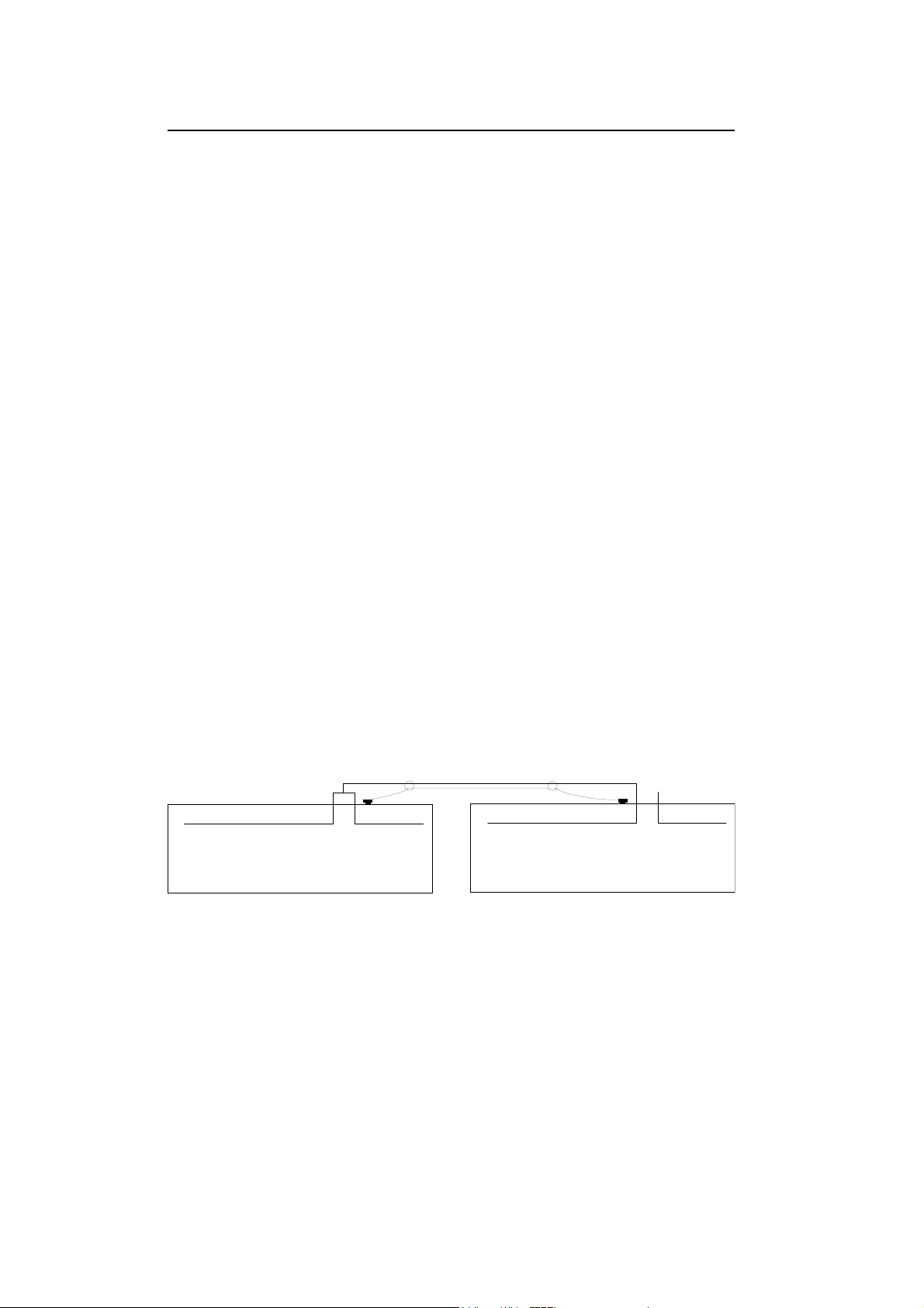
During unlinked operation a blanking plug must be inserted to
connect the input and output buses.
CD1308
This shows the Bus Link Blanking Plug.
CD1306
This shows the Bus Link PCB. There are two input connectors to
allow consoles where the master modules are located in the centre.
and one output connector. The output and input connectors are
connected by the blanking plug during normal (unlinked)
operation.
GROUND
STU D
BUS LINK PORT
BUS LINK PORT
GROUND
INPUT BUS OUTPUT BUS
MASTER CONSOLE
STU D
INPUT BUS OUTPUT BUS
SLA V E CONSO LE
42

THE METERBRIDGE
VU METERBRIDGE (CD1310)
The VU Meterbridge carries 11 meters indicating the three main
console outputs in addition to either the matrix, group or auxiliary
outputs of the console.
Signal selection is carried out by switches SW1 — SW3 while C1
ensures that on power up the GROUP signals will be displayed.
IC1 is a dual SR Flip Flop and normally the Reset input will be held
low by the pull down resitor R3. The Set input is wired to Vss and is
thus always low. When SW1 is pressed, or C1 is charging immediately
after switch on, Vdd is connected through D1 and R3 to Vss. Current
therefore flows and a voltage is created across R3 which is enought
to make the Reset input if IC1a see a logic high. The Q output is
thus set to a logic low while the Qbar output will be a logic high. A
similar situation will arise on IC1b and therefore the A and B control
inputs of the 4052 multiplexers will both be low allowing the X0
and Y0 input signals through which are the group signals. IC12a
also reads the control lines. As both are low and the IC is connected
as an invertor the output will go high causing LED1 to illuminate.
If neither or only one of the control lines is low the output will not
go high enough to turn on LED1.
If the matrix output is required then SW2 should be pressed. This
will cause C2 to charge through R1 creating a +ve pulse on the
clock input of IC1A. Assuming that we are in GROUP mode the
Data input will see the logic high from the Qbar output and this
will be clocked through to the Q output. The A control line now
goes high while the B control line stays low causing the multiplexers
to allow through the signals on the X1 and Y1 inputs which are the
matrix signals.
If the auxiliary outputs are required then SW3 should be pressed.
IC1B is clocked by a +ve going pulse from C3. Again the Data input
which is high will be clocked through to the Q output causing the
B control line to go high. The multiplexers will now allow through
signals connected to the X3 and Y3 inputs which are the auxiliary
output signals. The B control line is connected through to the RESET
pin of IC1A and when the auxiliary signal is selected a pulse will be
created through C6 causing IC1A to reset. When the auxiliary signals
are deselected the B control line will go low causing a -ve going
pulse. To prevent this from causing damage to the circuit
components it is clamped by D3 and thus prevented from driving
the reset pin more than 0.6V below ground. C7 and D4 perform
similar functions on IC1B.
43

When the A control line is high the output of IC11b will go low
causing the MATRIX indicator to illuminate while if the B control
line is high the output of IC12b will go low causing the Auxiliary
indicator to illuminate.
The outputs of the multiplexers are fed through buffer amplifiers
with some gain adjustment to allow for calibration of the meters.
Resistors attenuate the signal input to the multiplexers when a
signal is not selected in order to prevent breakthrough of any high
level audio signals. The signals for the left, centre and right mixes
do not travel through any multiplexers and are permanently
selected. There are of course only 6 matrix outputs and meters 7
and 8 will therefore not indicate during the period that the
meterbridge is being used to indicate MATRIX signals.
LED METERBRIDGE OUTPUT SIGNAL PROCESSING (CD1312)
The signal input to the led meterbridge output section is identical
to that of the VU meterbridge. Selection can be made between the
group, matrix and auxiliary signals. In this case the outputs from
the multiplexers are fed to quad comparator ICs of the type LM2901.
These rectify the audio signals and define the ballistics of the
resulting signal that is fed to the display board (CD1311).
LED METERBRIDGE OUTPUT DISPLA Y BOARD (CD1311)
Each meter is identical and is constructed from 3 quad comparator
ICs of the type LM2901 creating a 12 segment meter. A resistor
chain is used to set the threshold voltage for each comparator and
this determines the point at which an led will switch on. The leds
are driven from constant current sources formed from transistors
TR1 through TR8.
LED METERBRIDGE INPUT DISPLA Y BOARD (CD1307)
The meteres are identical to those used on the output display board
(CD1311). There is no need for a ballistics and rectifier section in
the meterbridge as the signal is taken from after the ballistics and
rectifier section of the meter driver on the module. Further LM2901
ICs (IC25 and IC26) are used to buffer the module signals before
being presented to the meters.
44

THE POWER SUPPL Y
The power supply is a linear type supplying +/-18 volts and +48
volts DC to the console. It may be rack mounted and a space of 2U
above the unit is recommended for ventilation.
The positive and negative rail regulators are identical in operation
thus only the positive rail is described.
Diodes D11 through D14 rectify the incoming AC from the
transformer and feed the main reservoir capacitors C9 and C10. A
small plug in module contains the series pass transistor and
associated regulating circuit. Q002 is the series pass transistor and
is driven from Q001 which in turn receives a control signal from
IC001, a 723. The output from the series pass transistor is passed
directly to the power supply output. D15 indicates that the supply
is functioning.
Diodes D1 through D4 rectify the AC used for the phantom voltage
supply. This is smoothed by C1, C2 and C4 from where it is fed to a
TL783C, the regulator. R1, R2 and R4 are used to derive a
programming voltage which is applied to the TL783C. D5 and D6
will protect the regulator from inverse voltages that may be applied
to it. C5 and C15 smooth the regulated output which is applied to
the output connector of the power supply. D7 indicates that the
phantom supply is working.
There is a delayed output from the power supply which may be
used to activate relays in a console. This facility is not used when
connected to the CS8 console.
There is no connection within the power supply between 0V and
mains earth (chassis). There is a ground lift switch which, when
operated, will allow the console to float completely free from
ground. If the ground is lifted then the console chassis is connected
to 0V Audio in the power supply.
DC Pinout
1 Not connected
2 +18 Volts
3 -18 Volts
4 0 Volts
5 +48 Volts
6 Chassis
The PSI2860 power supply is completely tested in accordance with
IEC65, 5th edition 1985 amendment number 1 and EMKO-TUE(12BSEC) 205/91.
45
Always connect the power supply to the console and the electricity
supply before switching on.
Fusing: 240/230/220V CSM02-0006 T3.15A
120/100/90V CSM02-0007 T6.3A
IMPORTANT: ALWAYS DISCONNECT THE POWER SUPPLY
FROM THE MAINS SUPPLY BEFORE OPENING.
REFER SERVICING TO A QUALIFIED PERSON OR DEALER
The PSI2860 will be factory set to the correct line voltage
although it may be changed altering the switches within the
unit.
240V
230V
220V
120V
100V
90V
POWER WIRING ONTO THE MASTER MODULE
1 BROWN +18v
2 N/C
3 GREEN 0V
4 BLUE -18v
5 GREEN/YELLOW CHASSIS
6 ORANGE PHANTOM
The chassis wire is bonded to the frame and also to a large
ground post on the rear panel of the console. In accordance with
current good practice pin 1 of the XLR connectors is taken to
chassis ground as is the sleeve connection from jack sockets.
46
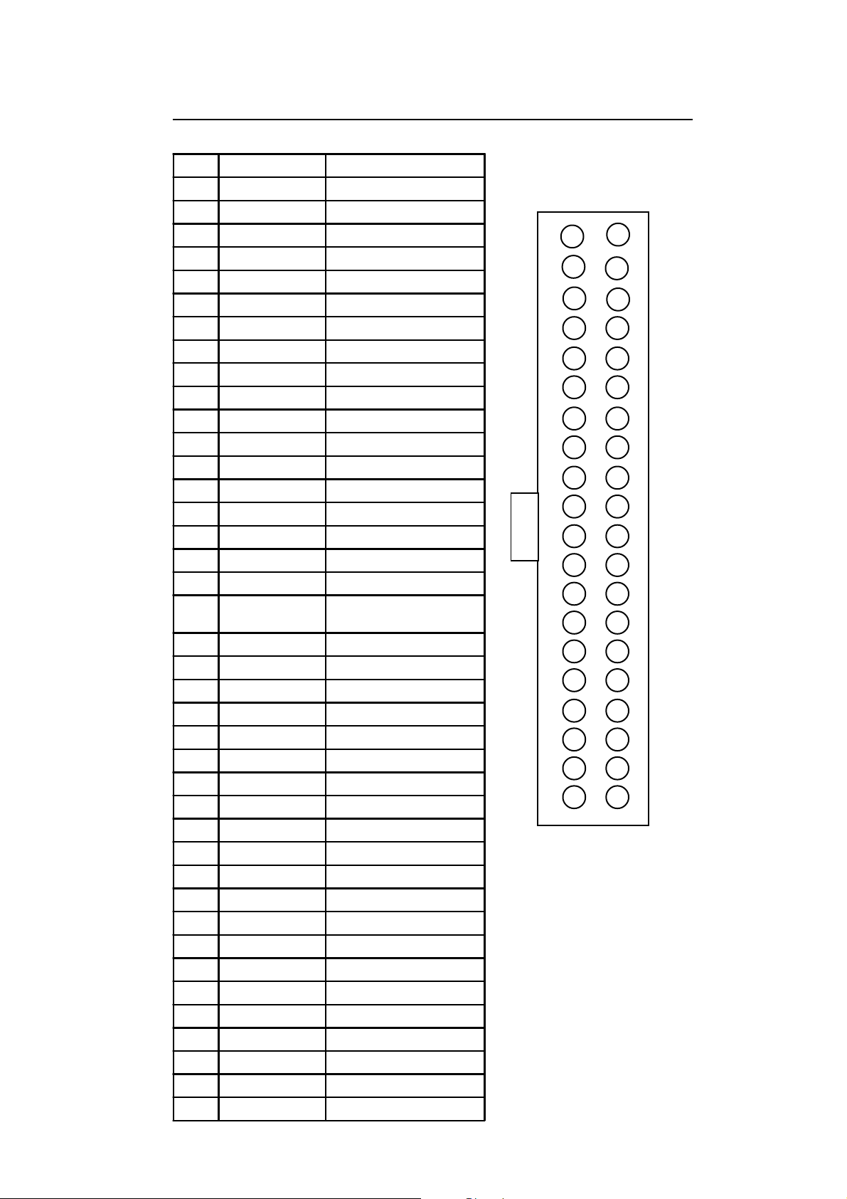
BUS CONNECTOR PIN OUT
PINSIGNAL DESCRIPTION
1BUS 8GROUP 8 BUS
2MUTE 1MUTE GROUP 1 BUS
3BUS 7GROUP 7 BUS
4MUTE 2MUTE GROUP 2 BUS
5BUS 6GROUP 6 BUS
6MUTE 3MUTE GRO UP 3 BUS
7BUS 5GROUP 5 BUS
8MUTE 4MUTE GROUP 4 BUS
9BUS 4GROUP 4 BUS
10 IPCU E INPUT CUE AUDIO
11 BU S 3GROUP 3 BUS
12 IPCUEDC INPUT CUE CO NTRO L
13 BUS 2GROUP 2 BUS
14 O PCUE O UTPU T CUE AUDIO
15 BU S 1GROUP 1 BUS
16 O PCU ED C O UTPUT CUE CO N TRO L
17 M IX RMIX RIGHT BUS
18 SIPSOLO IN PL ACE
19 M IX C
20 BU SREF BU S REF ERENCE
21 M IX LLEFT MIX BUS
22 +18V +18 VOLTS
23 AU X 8AUXILIARY 8 BUS
24 +18V +18 VO LTS
25 AU X 7AUXILIARY 7 BUS
26 +18V +18 VOLTS
27 AU X 6AUXILIARY 6 BUS
28 0V A U D IO GROUND
29 AU X 5AUXILIARY 5 BUS
30 0V A U DIO GROUND
31 A UX 4AUXILI ARY 4 BUS
32 0V A UDIO GRO UND
33 AU X 3AUXILIARY 3 BUS
34 -18V -18 VOLTS
35 AU X 2AUXILIARY 2 BUS
36 -18V -18 VOLTS
37 A U X 1AUXILIARY 1 BUS
38 -18V -18 VOLTS
39 M W KGRO UN D CHA SS IS
40 +48V PHA NTO M PO W ER
CENTRE OR MONO MIX
BUS
39
1
40
2
VIEW OF BUS RIBBON
CONNECTOR LOOKING
INTO THE CONSOLE
47

CS8 MA TRIX CONNECTO R
PINSIGNAL DESCRIPTION
1MTX 4MATRIX 4 BUS
2 M YX 5MATRIX 5 BUS
3MTX 3MATRIX 3 BUS
4MTX 6MATRIX 6 BUS
5MTX 2MATRIX 2 BUS
6MTX 7MATRIX 7 BUS
7MTX 1MATRIX 1 BUS
8MTX 8MATRIX 8 BUS
9MTX RMATRIX RIGHT BUS
10 REC-C CENTRE RECORD FEED
11 M TX CMATRIX CENTRE BUS
12 CM ON CENTRE MONITO R FEED
13 M TX LMATRIX LEFT BUS
1 4 GND AUDIO GR OUND
13
1
14
2
VIEW OF BUS RIBBON
CONNECTOR
LOOKING INTO THE
CONSOLE
48

BUS LINK CONNECTOR
DIN 41612 CO NN ECTO R
SIGNAL A B SIGNAL
BU S 81 1BUS 8
BU S 72 2BUS 7
BU S 63 3BUS 6
BU S 54 4BUS 5
BU S 45 5BUS 4
BU S 36 6BUS 3
BU S 27 7BUS 2
BU S 18 8 BUS 1
MIX R9 9MIX R
MIX C10 10MIX C
MIX L11 11MIX L
AUX 812 12AUX 8
AUX 713 13AUX 7
AUX 614 14AUX 6
AUX 515 15AUX 5
AUX 416 16AUX 4
AUX 317 17AUX 3
AUX 218 18AUX 2
AUX 119 19AUX 1
IPCU E 20 20 IPCU E
IPCU E DC 21 21 IPCU E DC
SIP2222SIP
BUS REF 23 23 BUS REF
0V 24 24 0V
0V 25 25 0V
0V 26 26 0V
0V 27 27 0V
MUTE 128 28MUTE 1
MUTE 229 29MUTE 2
MUTE 330 30MUTE 3
MUTE 431 31MUTE 4
MWK 32 32 MWK
49

CS8 P AR TS LISTING
This listing contains all the parts used in the assembley of a CS8 console. Where
possible both a DDA part number and an EVI part number are given and ultimately all
part numbers should be of the EVI type.
DDA No. DESCRIPTION EVI AUDIO P AR T NUMBER
ACBL17-005 .EART H LOOM ACBL17-1446-3
ACBL17-006 .EART H LOOM ACBL17-1447-3
ACBL17-009 .MASTER/COMMS WFM ACBL17-1450-3
ACBL17-010 .PSU XLR WFM ACBL17-1437-3
ACBL17-011 .LITTLITE XLR WFM ACBL17-1438-2
ACBL17-012 .HEADPHONE WFM ACBL17-1439-2
ACBL17-017 ..FADER W F M ACBL17-017-3
ACBL24-006 . M A TRIX LOOM ACBL24-1479-1
ACBL24-007 .MASTER/COMMS LINK WFM ACBL24-1440
ACBL24-008 .LITTLITE XLR’S WFM ACBL24-1504
ACBL24-010 ..F ADER W F M ACBL24-555
ACBL24-011 ..FADER W F M ACBL24-485
ACBL24-012 ..FADER W F M ACBL24-250
ACBL24-013 ..FADER W F M ACBL24-300
ACBL24-020 .O/P LED MTR WFM ACBL24-1480-1
ACBL24-021 .16CH L/H LED MTR WFM ACBL24-1481-1
ACBL24-025 .O/P VU MTR WFM ACBL24-1485-1
ACBL24-026 .VU METERBRIDGE WFM ACBL24-1486-1
ACBL24-030 .LOOM I/P 16CH LH ACBL24-1505-1
ACBL24-031 .LOOM I/P 24CH LH ACBL24-1506-1
ACBL24-032 .LOOM I/P 16CH RH ACBL24-1507-1
ACBL24-034 .LOOM I/P 24CH RH ACBL24-1509-1
ACBL24-035 .LOOM O/P ACBL24-1510-1
AMDL24-001 .STD I/P
AMDL24-004 .4+4 MONO/STEREO
AMDL24-012 .O/P & MASTER
APCB24-420 .CS8 BUS LINK - BLKG.PLUG
APCB24-421 .CS8 BUS LINK
CAP01-5002 ..33PF 50V 10%(5MM PITCH) CAP02-GK233050
CAP01-5003 ..100PF 5OV 10%(5MM PITCH) CAP02-GK310050
CAP01-5004 ..470PF 50V 10%(5MM PTCH) CAP02-GK347050
CAP01-5005 ..680PF 50V 10%(5MM PITCH) CAP02-GK368050
CAP01-5009 ..10PF 50V 5% (5MM PITCH) CAP02-GK210050
CAP01-5013 ..22OPF 50V 10%(5MM PITCH) CAP02-GK322050
CAP01-5014 ..150PF 50V 10%(5MM PTCH) CAP02-GK315050
CAP04-0010 ..220U 25V 20% (5MM PITCH) CAP43-322025
CAP04-0016 ..1000U 10V 20%(5MM PITCH) CAP43-410010
CAP04-0017 ..1000U 25V 20%(5MM PITCH) CAP43-410016
CAP04-5003 ..2U2 63V 20%(5MM PITCH) CAP43-122063
CAP04-5005 ..100U 16V 20%(5MM PITCH) CAP43-310016
CAP04-5006 ..22U 25V 20%(5MM PITCH) CAP43-222025
CAP04-5012 ..33U 63V 20%(5MM PITCH) CAP43-233063
CAP04-5026 ..2U2 50V 20%(5MM PITCH)LP CAP43-122050LP
50

DDA No. DESCRIPTION EVI AUDIO PAR T NUMBER
CAP04-5028 ..22U 25V 20%(5MM PITCH)LP CAP43-222025LP
CAP04-5031 ..1000U 10V 20%(5mmPTCH)LP CAP43-410010LP
CAP06-0001 ..1N CAP12-J110100
CAP06-0003 ..2N2 CAP12-J122100
CAP06-0005 ..4N7 CAP12-K147100
CAP06-0006 ..6N8 CAP12-J168100
CAP06-0007 ..10N 100V 5% CAP12-K210100
CAP06-0008 ..15N CAP12-J215100
CAP06-0010 ..33N CAP12-J233100
CAP06-0011 ..47N CAP12-J247100
CAP06-0012 ..68N CAP12-J268100
CAP06-0013 ..100N 63V 5% CAP12-J310100
CAP06-0015 ..220N 63V 5% CAP12-J322100
CAP06-0017 ..470N CAP12-J347100
CAP06-0025 ..330N 63V 10% 5MM CAP12-J333100
CON01-0008 ..3 W AY M E TWAY CON24-03MET
CON01-0027 . .O .1" 10 W A Y FML PCB MNT CON01-10SFV
CON01-0049 ..0.1" 3WY LKG ML HDR CON01-03SMVL
CON01-0055 ..0.1" 10WY V E R T EXT M/HDR CON01-10SMVX
CON01-0069 . .0.1" 2 W AY ML MOLEX CON01-02SMV
CON01-0069 . .0.1" 2 W AY ML MOLEX CON01-06SMVL
CON01-0075 ..0.1" 3WY R/A LKG MALE CON01-03SMRL
CON01-0079 ..0.156 3WY V E RT LK ML HDR CON02-03SMVL
CON01-0087 ..0.1" 6WY V E RT FML HDR CON01-06SFV
CON01-0116 ..0.156" 6WAY VERT ML HDR CON02-06SMVL
CON01-0123 ..0.1 6WA Y VE RT ML HDR(EX) CON01-06SMVX
CON01-0124 ..0.1 12WY R/A LKG ML HDR CON01-12SMRL
CON02-0016 .PLASTIC V E RT FML XLR CON31-X90203
CON02-0022 ..STEREO R/A PCB SLIM JACK CON32-S253-84
CON02-0029 ..DU A L P C PHONO VERT CON32-FC68405
CON02-0030 ..NC3 MAHL PLAS R/A ML PC CON31-3MAHL
CON02-0031 ..NC3 FAHL PLAS R/A FML PC CON31-3FAHL
CON02-0032 ..NC3 FAHR PLAS R/A FML PC CON31-3FAHR
CON02-0034 .NC4 FDL FML XLR CON31-4FDL1
CON03-0003 ..40WY R/A ML HDR CON11-40MHS
CON03-0051 ..16WY V E RT DIL ML HDR CON11-16MD
CON03-0064 ..14WAY R/A ML HDR CON11-14MHS
CON99-0015 ..0.25" R/A PCB BLADE CON84-025BLR
CON99-0016 .GROUND POST CON81-EFT51
CSM01-0008 ..24SWG LINKS WIR82-24SWG65
FRN04-0031 .REAN P&G KNOB - YELLOW FRN63-YEL11BLK
FRN04-0032 .REAN P&G KNOB - RED FRN63-RED11WHT
FRN04-0033 .REAN P&G KNOB - WHITE FRN63—WHT11BLK
FRN04-0034 .REAN P&G KNOB - BLACK FRN63-BLK11WHT
FRN04-0035 .REAN P&G KNOB - BLUE FRN63-BLU11WHT
FRN04-0036 .REAN P&G KNOB - GREEN FRN63-GRN11WHT
FRN06-0103 .REAN BLK/RED FRN32-BLK/RED
FRN06-0104 .REAN BLK/DK.GREY FRN32-BLK/GRY
FRN06-0106 .REAN LT.GREY/RED FRN32-GR Y/RED
51

DDA No. DESCRIPTION EVI AUDIO PAR T NUMBER
FRN06-0107 .REAN L T.GREY/BLUE FRN32-GRY/BLU
FRN06-0108 .REAN LT.GREY/GRN FRN32-GR Y/GRN
FRN06-0109 .REAN LT.GREY/BLK FRN32-GR Y/BLK
FRN06-0110 .REAN LT.GREY/LT.GRN FRN32-GR Y/LGN
FRN06-0111 .REAN BLK/LT GR N FRN32-BLK/LGN
FRN06-0113 .REAN LT.GREY/YELLOW FRN32-LGY/YEL
FRN06-0114 .REAN LT.GREY/DK.GREY FRN32-LGY/DGY
FRN06-0115 .REAN BLK/WHT FRN32-BLK/WHT
FRN07-0001 .SUJ GREY BLNK FRN41-PLGY
FRN07-0002 .SUJ GREY BLNK LED FRN41-LLGY
FRN07-0018 .SUJ GREY ‘DIR’ FRN41-PLGYDIR
FRN07-0019 .SUJ GREY ‘1-2’ FRN41-PLGY1-2
FRN07-0020 .SUJ GREY ‘3-4’ FRN41-PLGY3-4
FRN07-0021 .SUJ GREY ‘5-6’ FRN41-PLGY5-6
FRN07-0022 .SUJ GREY ‘7-8’ FRN41-PLGY7-8
FRN07-0030 .SUJ GREY ‘5’ FRN41-PLGY5
FRN07-0031 .SUJ GREY ‘6’ FRN41-PLGY6
FRN07-0033 .SUJ GREY ‘EQ’ FRN41-PLGYEQ
FRN07-0034 .SUJ GREY ‘MIX’ FRN41-PLGYMIX
FRN07-0097 .SUJ GREY ‘AFL’ LED FRN41-LLGY AFL
FRN07-0109 .SUJ GREY “ON” FRN41-PLGYON
FRN07-0112 .SUJ GREY “PFL” LED FRN41-LLGYPFL
FRN07-0121 .SUJ RED ‘MUTE’ LED FRN41-LREDMUTE
FRN07-0122 .SUJ RED ‘MUTE’ LED(REV) FRN41-RREDMUTE
FRN07-0130 .SUJ GREY ‘ P A N’ FRN41-PLGYP AN
FRN07-0131 .SUJ GREY ‘1’ FRN41-PLGY1
FRN07-0132 .SUJ GREY ‘2’ FRN41-PLGY2
FRN07-0133 .SUJ GREY ‘3’ FRN41-PLGY3
FRN07-0134 .SUJ GREY ‘4’ FRN41-PLGY4
FRN07-0135 .SUJ RED BLANK FRN41-PRED
FRN07-0136 .SUJ RED ‘CUT’ LED FRN41-LREDCUT
FRN07-0137 .SUJ RED LED BLANK FRN41-LRED
FRN07-0138 .SUJ GREY ‘MONO’ FRN41-PLGYMONO
FRN07-0139 .SUJ GREY ‘L/R’ FRN41-PLGYL/R
FRN07-0140 .SUJ GREY ‘7’ FRN41-PLGY7
FRN07-0141 .SUJ GREY ‘8’ FRN41-PLGY8
FRN07-0142 .SUJ GREY ‘STER’ FRN41-PLGYSTER
FRN07-0145 .SUJ GREY ‘ L’ FRN41-PLGYL
FRN07-0146 .SUJ GREY ‘R’ FRN41-PLGYR
FRN07-0147 .SUJ GREY ‘AFL’ LED(REV) FRN41-RLGYAFL
FRN07-0157 .SUJ GREY ‘SIS’ FRN41-PLGYSIS
FRN07-0159 .SUJ GREY ‘GAIN’ FRN41-PLGYGAIN
HWR01-0001 .M3 X 6 P/POZI BLK FAS01-M3006PPB
HWR01-0015 .M3 X 8 P/POZI BLK FAS01-M3008PPB
HWR01-0026 .NO6 X 21 MM FLANGE S/TAP FAS01-T0621FPZ
HWR01-0053 .M3 X 8 CSNK POZI BLK FAS01-M3008CPB
HWR01-0063 .NO4 X 3/8 P/POZI BLK FAS01-N0410PPB
HWR01-0081 .NO4 X 1/4 PAN BLK P/TITE FAS01-T0406PPB
HWR01-0083 .NO4 X 3/8 CSK POZI BLK FAS01-N0410CPB
52

DDA No. DESCRIPTION EVI AUDIO PAR T NUMBER
HWR01-0086 .M3 x 5mm PAN POZI BLK FAS01-M3005PPB
HWR01-0090 .2.5MM X 6 PAN BLK P/TECH F AS01-M2506PPB
HWR01-0091 .M4 X 8 PN.HD.SLT D.NYLON FAS01-M4008PSN
HWR02-0001 .M 3 N Y LO C F AS02-M30NZ
HWR02-0011 .M 4 N Y LO C F AS02-M40NZ
HWR02-0021 .M4 PLAIN W ASHER FAS03-M40FZ
HWR02-0022 .M4 S/PROOF W ASHER FAS03-M40SZ
HWR02-0034 .M4 NUT FAS02-M40FZ
HWR02-0036 .M5 S/PROOF W ASHER FAS03-M50SZ
HWR02-0041 .CHROME JACK NUT FAS02-REANJACK
HWR02-0043 .M3 NYLON W ASHER - BLAC K F AS03-M30PB
HWR02-0044 .11MM NYLON W ASHER-BLAC K FAS03-U11FN
HWR99-0010 .RS H15 SLEEVE 397-720 WIR92-S H15x20
HWR99-0011 .RS H20 SLEEVE 397-736 WIR92-S H20x20
HWR99-0072 .MODL MOUNTING CLIP (SML) FAS41-SNU1812
HWR99-0080 .METERBRIDGE FIXING CLIP FAS41-335106
HWR99-0092 ..LED HOLDER 8 W AY HWR99-DUH368
HWR99-0093 ..LED HOLDER 4 W AY HWR99-DUH364
HWR99-0099 .FOOT (21MM DIA) HWR42-FF-000P4
HWR99-0100 .M3 X 14MM PILLAR HWR12-M3014CPN
HWR99-0113 .M3 X 18MM PILLAR(M/FM) HWR12-M3018BP
HWR99-0115 .DOME PLUG(6MM)-BLACK HWR06-DP250
MTR01-0005 .AL29 METER MTR11-AL29
MTR99-0010 .LIGHT BOX FOR AL29 MTR19-AL29BOXA
MWK24-0004 .O/P & CONN PANEL
MWK24-0006 .MASTER & CONN P ANEL
MWK24-0008 .16CH FRAME MWK24-2328-1
MWK24-0009 .24CH FRAME MWK24-2329-1
MWK24-0010 .32CH FRAME MWK24-2330-1
MWK24-0011 .40CH FRAME MWK24-2331-1
MWK24-0012 .48CH FRAME MWK24-2332-1
MWK24-0013 .L/H CLADDING MWK24-2333-1
MWK24-0014 .R/H CLADDING MWK24-2334-1
MWK24-0015 .16CH ARMREST MWK24-2335-1
MWK24-0016 .24CH ARMREST MWK24-2336-1
MWK24-0017 .32CH ARMREST MWK24-2337-1
MWK24-0018 .40CH ARMREST MWK24-2338-1
MWK24-0019 .48CH ARMREST MWK24-2339-1
MWK24-0020 .4+4 MONO/STEREO P ANEL MWK24-2342-1
MWK24-0024 .VU O/P M/BRIDGE PANEL MWK24-2349-1
MWK24-0026 .VU O/P M/BRIDGE FACIA MWK24-2351-1
MWK24-0027 .16CH LED M/BRIDGE MWK24-2357-1
MWK24-0028 .16CH M/BRIDGE COVER MWK24-2359-2
MWK24-0029 .16CH LED M/BRIDGE FACIA MWK24-2372-1
MWK24-0030 .24CH LED M/BRIDGE MWK24-2360-1
MWK24-0031 .24CH M/BRIDGE COVER MWK24-2362-2
MWK24-0032 .24CH LED M/BRIDGE FACIA MWK24-2373-1
MWK24-0033 .32CH LED M/BRIDGE MWK24-2363-1
MWK24-0034 .32CH LED M/BRIDGE COVER MWK24-2365-2
53

DDA No. DESCRIPTION EVI AUDIO PAR T NUMBER
MWK24-0035 .32CH LED M/BRIDGE FACIA MWK24-2374-1
MWK24-0036 .40CH LED M/BRIDGE MWK24-2366-1
MWK24-0037 .40CH LED M/BRIDGE COVER MWK24-2368-2
MWK24-0038 .40CH LED M/BRIDGE FACIA MWK24-2375-1
MWK24-0039 .48CH LED M/BRIDGE MWK24-2369-1
MWK24-0040 .48CH LED M/BRIDGE COVER MWK24-2371-2
MWK24-0041 .48CH LED M/BRIDGE FACIA MWK24-2376-1
MWK24-0042 ..SWITCH CAP(TP2301) FRN58-2301BLK
MWK24-0043 .L/H CLADDING - M/BRIDGE MWK24-2352-1
MWK24-0044 . R /H C L AD D ING - M/BRIDGE MWK24-2353-1
MWK24-0045 . O/P & MASTER CONN PNL MWK24-2380-1
MWK24-0046 .2CH BLANK PANEL MWK24-2381-1
MWK24-0048 . METER I/FA C E BLANK PNL
MWK99-0040 .LOCATING PCB MTG BRKT MWK99-2273-4
MWK99-0049 .PCB MOUNTING BRKT MWK99-2379-1
MWK99-0050 .MULTICORE BLANKING PLUG MWK99-2346-1
MWK99-0051 .BUS LINK COVER PNL MWK99-2378
PCB17-1385 ..METER
PCB24-1394 ..CS8 STD INPUT
PCB24-1395 ..CS8 STD OUTPUT
PCB24-1396 ..CS8 MASTER
PCB24-1397 ..CS8 COMMS
PCB24-1398 ..CS8 MATRIX
PCB24-1413 ..CS8 STD INPUT SUB
PCB24-1418 ..CS8 STEREO INPUT
PCB24-1419 ..CS8 STEREO INPUT SUB
PCB24-1423 ..CS8 INPUT METERBRIDGE
PCB24-1424 ..CS8 OUTPUT LED MB
PCB24-1425 ..CS8 OUTPUT LED MB SUB
PCB24-1426 ..CS8 VU METER DRIVER
POT02-0006 ..1/4" 5K HORIZ. TRIMMER POT32-503H
POT02-0010 .1/4" 500R HORIZ. TRIMMER POT32-502H
POT02-0012 .1/4" 500R V E RT. TRIMMER POT32-502V
POT02-0013 .1/4" 5K V E RT. TRIMMER POT32-503V
POT03-0021 .ALPS N 100MM R/A MONO POT2N-10M14JR
POT03-0022 .ALPS N 100MM R/A STEREO POT2N-10S14JRA
POT04-0013 .ALPS 10KA X 3 POT93-414A01
POT05-0001 .5KRD X 2 REV LOG POT14-653D02
POT05-0002 .10KB LIN C/D POT11-614B01D
POT05-0003 .10KB X 2 LIN C/D POT14-614B01D
POT05-0004 .20KA LOG POT11-624A01
POT05-0005 .100KC X 2 INV LOG POT14-615C01
POT05-0006 .10KA LOG POT11-614A01
POT05-0007 .10KA X 2 LOG POT14-614A01
POT05-0008 .10KRD REV LOG POT11-614RD
POT05-0009 .5KB X 2 LIN C/D C/T POT14-653Z26C
POT05-0101 .5KRD X 2 REV LOG(N/B) POT14-653D02N
POT05-0102 .10KB LIN C/D(N/B) POT11-614B01DN
POT05-0103 .10KB X 2 LIN C/D(N/B) POT14-614B01DN
54

DDA No. DESCRIPTION EVI AUDIO PAR T NUMBER
POT05-0104 .20KA LOG(N/B) POT11-624A01N
POT05-0105 .100KC X 2 INV LOG(N/B) POT14-615C01N
POT05-0106 .10KA LOG(N/B) POT11-614A01N
POT05-0107 .10KA X 2 LOG(N/B) POT14-614A01N
POT05-0108 .10KRD REV LOG(N/B) POT11-614RDN
POT05-0109 .5KB X 2 LIN C/D C/T(N/B) POT14-653Z26CN
POT05-0110 .20KB LIN (N/B) POT11-624B01N
POT05-0111 .20KB X 2 LIN (N/B) POT14-624B01N
RES01-0001 ..10R RES01-1E1R00
RES01-0025 ..100R RES01-2E1R00
RES01-9997 ..1R5 RES01-0E1R50
RES01-9999 ..1R RES01-0E1R00
RES03-0006 ..100R 4W W/W RES11-040310
RES03-0013 ..22R 4W 5% CERAMIC RES11-040222
RES04-0002 ..10R RES04-1E1R00
RES04-0010 ..22R RES04-1E2R20
RES04-0011 ..27R RES04-1E2R70
RES04-0013 ..33R RES04-1E3R30
RES04-0017 ..47R RES04-1E4R70
RES04-0021 ..68R RES04-1E6R80
RES04-0022 ..75R RES04-1E7R50
RES04-0025 ..100R RES04-2E1R00
RES04-0026 ..120R RES04-2E1R20
RES04-0027 ..150R RES04-2E1R50
RES04-0029 ..180R RES04-2E1R80
RES04-0033 ..240R RES04-2E2R40
RES04-0035 ..270R RES04-2E2R70
RES04-0036 ..300R RES04-2E3R00
RES04-0037 ..330R RES04-2E3R30
RES04-0038 ..360R RES04-2E3R60
RES04-0041 ..470R RES04-2E4R70
RES04-0042 ..510R RES04-2E5R10
RES04-0047 ..820R RES04-2E8R20
RES04-0048 ..910R RES04-2E9R10
RES04-0049 ..1K RES04-3E1R00
RES04-0051 ..1K2 RES04-3E1R20
RES04-0053 ..1K5 RES04-3E1R50
RES04-0054 ..1K6 RES04-3E1R60
RES04-0055 ..1K8 RES04-3E1R80
RES04-0056 ..2K RES04-3E2R00
RES04-0057 ..2K2 RES04-3E2R20
RES04-0059 ..2K7 RES04-3E2R70
RES04-0060 ..3K RES04-3E3R00
RES04-0061 ..3K3 RES04-3E3R30
RES04-0062 ..3K6 RES04-3E3R60
RES04-0063 ..3K9 RES04-3E3R90
RES04-0065 ..4K7 RES04-3E4R70
RES04-0066 ..5K1 RES04-3E5R10
RES04-0067 ..5K6 RES04-3E5R60
55

DDA No. DESCRIPTION EVI AUDIO PAR T NUMBER
RES04-0068 ..6K2 RES04-3E6R20
RES04-0069 ..6K8 RES04-3E6R80
RES04-0070 ..7K5 RES04-3E7R50
RES04-0072 ..9K1 RES04-3E9R10
RES04-0073 ..10K RES04-4E1R00
RES04-0074 ..11K RES04-4E1R10
RES04-0075 ..12K RES04-4E1R20
RES04-0077 ..15K RES04-4E1R50
RES04-0079 ..18K RES04-4E1R80
RES04-0080 ..20K RES04-4E2R00
RES04-0081 ..22K RES04-4E2R20
RES04-0082 ..24K RES02-3E2R40
RES04-0083 ..27K RES04-4E2R70
RES04-0085 ..33K RES04-4E3R30
RES04-0089 ..47K RES04-4E4R70
RES04-0091 ..56K RES04-4E5R60
RES04-0093 ..68K RES04-4E6R80
RES04-0097 ..100K RES04-5E1R00
RES04-0101 ..150K RES04-5E1R50
RES04-0103 ..180K RES04-5E1R80
RES04-0105 ..220K RES04-5E2R20
RES04-0106 ..240K RES04-5E2R40
RES04-0107 ..270K RES04-5E2R70
RES04-0109 ..330K RES04-5E3R30
RES04-0113 ..470K RES04-5E4R70
RES04-0116 ..1M RES04-6E1R00
RES04-0117 ..2M2 RES04-6E2R20
RES04-0118 ..680K RES04-5E6R80
RES04-0122 ..1M5 RES04-6E1R50
RES04-0123 ..4M7 RES04-6E4R70
RES04-0124 ..4R7 0.4W 1% RES04-0E4R70
RES04-0128 ..820K RES04-5E8R20
RES04-9999 ..‘0’R LINK RES04-0E0R00
SEM01-0001 .STD 3MM GREEN SEM01-5130GDA
SEM01-0002 .STD 3MM RED SEM01-5129RDA
SEM01-0012 .STD 3MM YELLOW SEM01-5131YDA
SEM01-0031 .LED LIGHT BAR RED SEM02-KB2685EW
SEM02-0001 .1N4148 SEM11-1N4148
SEM02-0002 .1N4002 SEM11-1N4002
SEM02-0007 .6.8V ZENER SEM12-ZX79V068
SEM02-0008 .9.1V ZENER SEM12-ZX55V091
SEM02-0009 .22V ZENER SEM12-ZX79V220
SEM02-0014 .5.1V ZENER SEM12-ZX79V051
SEM02-0016 .16V ZENER SEM12-ZX79V160
SEM02-0018 .18V ZENER SEM12-ZX55V180
SEM02-0028 .8V2 ZENER (1.3 W ATTS) SEM12-ZX85V082
SEM03-0007 .8A 100V BRIDGE SEM21-KBU802
SEM04-0004 .BC182/547 SEM31-BC182
SEM04-0005 .BC212/557 SEM31-BC212
56

DDA No. DESCRIPTION EVI AUDIO PAR T NUMBER
SEM04-0010 .J111 N JFET SEM33-J111
SEM04-0015 .TIP32C(TO220) SEM32-TIP32C
SEM04-0021 .ZTX453 SEM32-ZTX453AI
SEM04-0022 .ZTX553 SEM32-ZTX553AI
SEM04-0023 .TIP31C SEM32-TIP31C
SEM04-0024 .BC182(TO92 TAPE)5MM PTCH SEM31-BC182AI
SEM04-0025 .2SB737(TO92 TAPE)5MM PCH SEM31-2SB737AI
SEM04-0026 .J176(TO92 TAPE)5MM PITCH SEM33-J176AI
SEM04-0027 .BC212(TO92 TAPE)5MM PTCH SEM31-BC212AI
SEM04-0028 .J111(T092 TAPE)5MM PITCH SEM33-J111AI
SEM06-0002 .TL072CN SEM41-TLO72CN
SEM06-0004 .NE5534 SEM41-NE5534
SEM06-0009 .NE5532P SEM41-NE5532
SEM06-0038 .CD4013BCN SEM42-CD4013
SEM06-0074 .SSM2017 MIC AMP SEM41-SSM-2017
SEM06-0076 .BA683A 12 LED MTR DRIVER SEM41-BA683A
SEM06-0103 .LM2901 QUAD COMPAR ATO R SEM41-2901
SEM06-0169 .4052 SEM42-CD4052
SWT01-0004 .2 POLE SUJ SWT01-SUJ2LC
SWT01-0005 .4 POLE SUJ SWT01-SUJ4LC
SWT01-0006 ..6 POLE SUJ SWT01-SUJ6LC
SWT01-0031 ..SUJ 4 POLE (MOM) SWT01-SUJ4MC
SWT01-0033 ..TP2301 SWT04-TP23MOV
SWT02-0004 .MAINS SWITCH (UL) SWT32-2B10
SWT99-0020 .THERMAL SWITCH (100/85C) SWT81-100CNO
TMR99-0002 ..FERRITE BEAD INDUCTOR TMR21-BEADLINK
WIR02-0010 ..WHITE WIR01-WHITE
57

SER VICE INFORMA TION
With the exception of the meters there are no adjustments within
the CS8 console.
SAFETY
Always switch off the console before carrying out any work on it.
TOOLS
No special tools are required in order to service the CS8. An
oscilloscope and multimeter will allow fault finding to component
level in the unlikely event of a fault. A module extension cable,
ACBL99-023, is supplied with the console to enable individual
channels to be powered when removed from the frame. If a
complete block of 8 channels is to be serviced then ACBL99-024, an
8 way extension cable, should be used.
MODULE REMOVAL
Remove the twelve screws retaining a module and ease it out of
the frame. There are four screws at the bottom of the module,
four screws at the top of the module and four screws at the rear of
the console at the base of the connector panel. The recommended
method is to raise the front of the module and to push the module
a little towards the front of the console from the rear connector
panel. Lift the module, holding it at the front edge and rear
connector panel. Keep it parallel to the front plane of the console
and disconnect the ribbon cable from each of the 8 boards before
pulling the module completely clear.
MODULE DISASSEMBL Y
Remove the screws mounting the XLR to the connector panel.
Remove the screws holding the circuit board to the top panel and
pull the circuit board clear.
MODULE REASSEMBL Y
This is a reverse of the disassembly process and care must be taken
that leds are not damaged through misalignment with their panel
holes.
MODULE REPLACEMENT
Place the module over its final position and reconnect the ribbon
cable to all the boards. Gently ease the module back into the frame
taking care not to crush or otherwise damage the ribbon cable.
Insert the 12 retaining screws.
ST A TIC PRECAUTIONS
Electronic equipment can be very sensitive to static discharges and
care should be taken to avoid static in the work area. Where possible
work on a bench where you can be grounded through a wrist strap.
58

If boards have to be shipped then they should be wrapped in
conductive plastic bags or conductive plastic sheeting.
PAR TS
In the interests of safety always use genuine replacement parts.
Safety approvals will be invalidated by use of non standard
components.
METER ALIGNMENT
An audio test set is required to accurately measure the level of the
output for which the meter is being adjusted.
Master Left and Right Meters
With 0dBu at the console outputs adjust PR1 to read 0dB and with
-21dBu at the console output adjust PR2 such that the bottom led
is just on. These adjustments should be repeated until both readings
are accurate as they are interactive to some extent.
Centre Meter
PR15 should be used to set the 0dB point while PR25 should be
used to set the -21dB point following the above procedure.
Group Meters
PR2 should be used to set the 0dB point while PR3 should be used
to set the -21dB point following the above procedure.
If a meterbridge is fitted then some additional calibration work
will be required as follows:-
VU Bridge
Calibrate the console meters as above and then use PR1 through
PR7 to calibrate the VU meters. The adjustment is the same for
whichever signal source is selected and it is therfore probably easiest
to set the meters to read GROUP. Set the group outputs to +4dBu
(0VU) and adjust PR1 for group 1 so that the meter reads 0VU.
Calibrate the remaining meters using PR2 through PR8.
The master meters can be set in the same fashion having set the
output levels to +4dBu. PR9 will calibrate the left meter while PR10
and PR11 will calibrate the centre and right meters respectively.
LED Bridge
There are no adjustments in the led meterbridge.
59

CS8 CIRCUIT DIAGRAMS
MODULE CIRCUIT PCB
INPUT MODULE CD1279 PC1394/PC1413
STEREO INPUT MODULE CD1302 PC1418/19
CD1303 PC1418/19
GROUP MODULE (1-6) CD1286 PC1395
GROUP MODULE (7-8) CD1280 PC1398
MASTER MODULE (MASTER MIX) CD1281 PC1396
MASTER MODULE (T APE/SOLO) CD1282 PC1396
MASTER MODULE (CENTRE MIX) CD1283 PC1397
MASTER MODULE (T/B MONITOR) CD1284 PC1397
CENTRE METER CD1273 PC1385
POWER SUPPL Y CD1271 PC1386
BUS LINK CD1306 PC1421
BUS LINK BLANKING PLUG CD1308 PC1420
LED INPUT METER CD1307 PC1423
LED OUTPUT METER CD1311 PC1424
LED OUTPUT METER SUB PCB CD1312 PC1425
VU METER CD1310 PC1426
METER CONNECTOR CD1309 PC1422
60
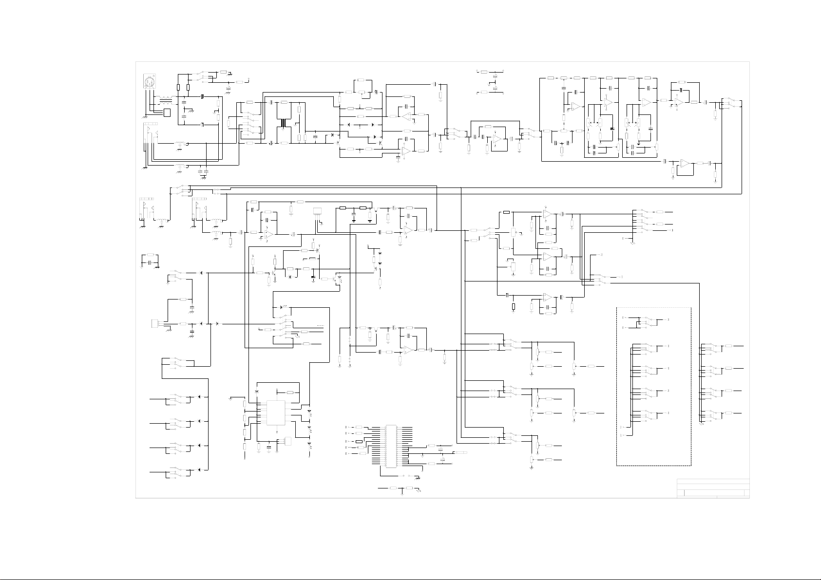
MIC
CON2
NC3FAHL
R3
6K8R26K8
231
SP6
CM-CHOKE
1 2
3 4
CON9
3
2
1
3WAY
MH
CON5
1/4JACKSL
DIRECT
OUT
R87
100R
C30
10N
213456
EXTERNAL
CUT
MUTE1
MUTE2
MUTE3
MUTE4
CON3
1/4JACKSL
LINE
213456
SP1
1N
SP2
1N
DIRECT
PRE
SW28
2PSUJ
SP5
1N
CUT
SW16
2PSUJ
CON7
1
2
3
3WAY
MHR/A
SAFE
SW17
2PSUJ
MUTE 1
SW18
2PSUJ
MUTE 2
SW19
2PSUJ
MUTE 3
SW20
2PSUJ
MUTE 4
SW21
2PSUJ
This drawing is split across the following two pages to aid readability .
+48V
R4
SW1
47K
+48V
R1
R5
10K
10K
1 2
1 2
SP3
1N
SP4
1N
470R
C1
MIC/
2U2
63V0.2
LINE
GAIN
R7
C45
4K7
100U
16V0.2
R6
LK11
LK12
D8
1N4148
SW2
R9
300R
4PSUJ
C46
R8
100U
16V0.2
4K7
NOTE: IF T1 IS FITTED
R14 CHANGES TO 1K AND
R10 AND R11 ARE NOT FITTED.
R140
470K
C63
R108
100P
10K
C18
33P
V-
R136
C19
4
IC7A
INS_RET
2
3
10K
100U
16V0.2
R133
100K
R94
47K
R95
22K
V+ R135
NE5532
8
V+
R97
270K
TR6
BC182
R96
22K
47K
2PSUJ
C2
33U
C37
63V0.2
680P
C38
680P
C3
33U
63V0.2
C40
C39
680P
680P
POST
PRE
CON4
1/4JACKSL
213456
INSERT
D6
1N4148
R92
1K
C60
100P
D7
R129
1N4148
1K
C59
100P
1
V+V+
8 2
6 4
SOLO
MIC/LINE GAIN
R10
*
10R
R12
24K
(OPT)
NTM1
1
T1
*
R14
R13
C4
24K
24K
680P
*
R11
*
10R
GAIN = 20 TO 70dB
OR -10 TO +20dB
INS_SEND
R142
470K
WIR2
R141
1K2
100U
16V0.2
LED2
YEL
SW22
4PSUJ
3WAY
123
C20
V+
R144
V+
100K
R107
TR4
BC212
470K
R130
V-
470K
R118
R98
680K
220K
D10
1N4148
R37
C36
220N
47K
SIP
R134
IPCUEDC
47K
IPCUE
10K
R93
DO NOT FIT
R145
6K2OPT
VR1
C5
10KRDR16
1 2
10R
1000U
3
R15
150R
D2
1N4148
D1
1N4148
TR7
2SB737
R50
7K5
TR3
LED1
RED
BC182
LK1
LK03
R146
1M
6.3V
V1+
R110
R109
7K5
7K5
R111
56K
V1-
R112
4K7
V1-
R39
7K5
C51
100P
R99
15K
R100
1
2
2
LK2
LK03-OPT
1
R123
7
IC1B
75R
NE5532
D4
1N4148
D3
1N4148
TR5
V1-
2SB737
R113
4K7
R38
7K5
V+
R88
150R
BC212
7K5
TR8
TR1
J176
220P
R89
10K
TR2
J176
150P
R119
100K
R412KC32
D9
1N4148
D15
1N4148
V-
R120
100K
C35
R102
2K
2
3
C47
33P
V1+
C49
100U
16V0.2
2
3
R42
33R
CHANNELCUT
C50
100U
16V0.2
6
5
R103
27R
C53
100U
16V0.2
R117
R121
100K
3K3
C56
33P
R116
6
5
R115
56K
C48
10P
4
IC1A
1
NE5532
8
R40
47K
C43
10P
V-
4
IC4A
1
NE5532
8
V+
R101
15K
C33
33P
IC7B
7
NE5532
PHASE
REVERSE
3K3
C6
100U
16V0.2
R122
100K
R114
75R
C44
R104
75R
220U
25V
C34
R105
75R
100U
16V0.2
R131
100K
SW3
2PSUJ
PRE1
POST
R85
V+ V1+
0R
R86
0R
R19
V+
10K
C7
C8
3
2
100N
100N
R18
R17
V-
33K
100K
HIGH PASS FILTER
18dB/OCTAVE, 80Hz
LCR
MODE
SW15
R59
1K6
R65
2PSUJ
1K
POST
LK4
1 2
PRE1
LK3
1 2
PRE2
C41
220U
25V
C42
220U
25V
V1-V-
8
C9
1
IC2A
2U2
4
TL072
63V0.2
R51
1K6
2
CW
3 7
1
VR16A
5KB
X2NB
R52
2K2
5
CW
6
VR16B
5KB
X2NB
4
C26
220N
R60
680K
PRE
SW6
2PSUJ
AUXILIARY CUT
PRE
SW7
V+
D5
R49
D11
1N4148
D12
1N4148
D13
1N4148
D14
1N4148
1N4148
10K
3
5
2
+
R44
680R
R45
6K8
R46
47K
R48
R47
820K
47K
V+
O
+
4
V
-
7
1
+
O
6
-
9
+
O
8
-
11
+
O
-
10
-
V
12IC6
LM2901
V-
C21
330N
EXT METER
LED3
SIG
GRN
14
13
LED4
YEL
CON8
1
2
LED5
3
RED
3WAY
MH
V-
0Vu
PEAK
5
R72 10K
4
R70 10K
3
R68 10K
2
R66 10K
1
R64 10K
CON1
BUS8
BUS6
BUS4
BUS2
MIXR
MIXL
AUX8
AUX7
AUX6
AUX5
AUX4
AUX3
AUX2
AUX1
MUTE1
12
MUTE2
34
MUTE3
56
MUTE4
78
IPCUE
910
IPCUEDC
11 12
opcue
13 14
opcuedc
15 16
17 18
19 20
21 22
23 24
25 26
27 28
29 30
31 32
33 34
35 36
37 38
39 40
40WAY
IDCMH
DO NOT FIT
1 2
CLEAN 0V
R82
BUSREF
120R
R80
SIP
BUSREF
+18V
0V
0V
0V
-18V
L70
+48V
LK04
R83
0R
10R C28
R81
10R
V+
220U
2 PL1
25V
1
1/4"RPB
C29
220U
25V
V-
1 2
1 2
1 2
1 2
LK5
LK6
2PSUJ
PRE
SW8
LK7
LK8
2PSUJ
HF/LF EQ
R21
1K5
HIGH
PASS
SW4
R24
1K8
C12
2PSUJ
R20
470N
10K
PAN BUFFER
R143
3K
V+
IC5A
8
TL072
3
1
2
4
V-
R53
C22
5K6
33P
R138
3K6
R139
1M5
R54
1M5
5
7
6
IC5B
TL072
C24
R56
33P
5K6
R57
3K6
IC4B
NE5532
5
7
6
C31
R90
33P
5K6
R91
4K7
VR8
2
20KA
R74
3
AUX1
10K
1
2
R75
3
AUX2
10K
VR9
20KA
1
AUX1/2 AUX3
VR11
20KA
2
R77
3
AUX4
10K
1
2
R78
3
AUX5
10K
VR12
20KA
1
AUX4/5 AUX6
VR14
20KA
2
R127
3
AUX7
10K
1
2
R128
3
AUX8
10K
VR15
1
20KA
AUX7/8
VR2
10KB
3
C10
2N2
6
5
R23
22K
3
VR7
10KB
C64
470N
C23
100U
16V0.2
R55
100K
C25
100U
16V0.2
R58
100K
C27
100U
16V0.2
R61
100K
MID EQ
R26
R22
1 2
10K
1K5
C11
33P
2
IC2B
3
7
TL072
4
1
6
3
5
2
R25
VR3A
1 2
100KC
1K8
R35
3K
C14
4N7
C61
470P
PANL
PANR
PAN
GROUPS
SW14
2PSUJ
PANC
2
R76
3
AUX3
VR10
10K
20KA
1
2
R79
3
AUX6
VR13
10K
1
20KA
R27
10K
33P
V-
4
8
V+
VR3B
100KC
R34
3K
7
TO
C13
IC3A
1
TL072
C15
2N2
2
3
VR4
10KB
1
9
8
Snap-Off Sub Board
6S
7S
8S
9S
1
2
R29
10K
6
VR5A
100KC
R124
3K
C54
MID EQ
3
33N
C62
2N2
6
5
4
VR5B
100KC
5
R125
3K
R30
10K
C57
33P
IC3B
7
TL072
C55
15N
3
VR6
10KB
SW13
4PSUJ
SW27
2PSUJ
SW23
2PSUJ
SW24
2PSUJ
SW25
2PSUJ
SW26
2PSUJ
LAST R
LAST C
LAST CON
LAST D
LAST LED
LAST IC
LAST SW
LAST VR VR16
LAST LK
R32
3K3
C16
33P
V-
R31
4
3K3
2
R126
1
3
IC8A
75R
NE5532
8
V+
2
1
R62
10K
R63
10K
C58
220N
R33
680K
MIX
MIXL
MIXR
CENTRE
BUS1
BUS3
BUS5
BUS7
R146
C63
CON9
D15
LED5
IC8
SW28
LK12
R28
5
7
6
75R
IC8B
NE5532
6
1S
2S
3S
4S
5S
DDA, HOUNSLOW, MIDDX, TW3 2EB, ENGLAND.
Title
Size Document Number REV
D CD1279-1 A
Date: March 7, 1997 Sheet 1 of 1
EQ IN
SW5
C52
100U
16V0.2
2PSUJ
R137
100K
C17
100U
16V0.2
R36
100K
SW9
R67
BUS2
10K
BUS2
2PSUJ
SW10
R69
BUS4
10K
BUS4
2PSUJ
SW11
R71
BUS6
10K
BUS6
2PSUJ
SW12
R73
BUS8
10K
BUS8
2PSUJ
CS8 INPUT

MIC
CON2
NC3FAHL
231
SP6
CM-CHOKE
1 2
3 4
CON9
3
2
1
3WAY
MH
CON3
1/4JACKSL
LINE
213456
+48V
SW1
R3
6K8
SP1
1N
SP2
1N
2PSUJ
R2
6K8
33U
C37
63V0.2
680P
C38
680P
63V0.2
C40
680P
R4
47K
C2
R5
10K
R6
10K
C3
33U
C39
680P
+48V
R1
470R
C1
MIC/
2U2
63V0.2
LINE
GAIN
R7
4K7
R9
300R
R8
4K7
16V0.2
SW2
4PSUJ
NOTE: IF T1 IS FITTED
R14 CHANGES TO 1K AND
R10 AND R11 ARE NOT FITTED.
C45
100U
8 2
6 4
C46
100U
16V0.2
(OPT)
NTM1
*
R10
*
10R
1
T1
R11
*
10R
MIC/LINE GAIN
R12
24K
R14
R13
24K
24K
*
C4
680P
GAIN = 20 TO 70dB
OR -10 TO +20dB
D1
1N4148
2SB737
DO NOT FIT
R145
6K2OPT
VR1
R16
10R
R15
150R
R109
7K5
D2
1N4148
R112
4K7
C5
10KRD
1 2
1000U
3
6.3V
V1+
R110
7K5
R111
56K
D4
1N4148
V1-
D3
1N4148TR7
TR5
2SB737
R113
4K7
V1-
R117
3K3
C56
33P
6
R123
7
5
IC1B
75R
NE5532
R115
56K
C48
10P
V1-
4
IC1A
2
1
3
NE5532
8
C47
33P
V1+
C53
100U
16V0.2
R121
100K
R116
3K3
C6
100U
16V0.2
R114
75R
SW3
2PSUJ
R122
100K
PHASE
R19
10K
V+
C7
C8
8
3
2
100N
100N
4
TL072
R18
R17
100K
V-
33K
HIGH PASS FILTER
18dB/OCTAVE, 80Hz
HF/LF EQ
VR2
10KB
R21
1K5
HIGH
PASS
SW4
R24
2PSUJ
V+ V1+
1K8
470N
R143
R85
0R
R86
0R
C9
1
IC2A
2U2
R20
63V0.2
10K
R22
1 2
1K5
3
C10
C11
2N2
33P
6
5
R23
22K
3
1 2
VR7
10KB
C12
C64
470N
3K
C41
220U
25V
C42
220U
25V
V1-V-
MID EQ
HI LO
R26
10K
IC2B
7
TL072
1
3
6
2
R25
VR3A
100KC
1K8
R35
3K
C14
4N7
C61
470P
BUSREF
R27
10K
33P
V-
4
2
3
8
V+
4
VR3B
100KC
5
R34
3K
R82
120R
R29
R30
10K
10K
C13
IC3A
1
TL072
C15
2N2
2
3
VR4
10KB
1
R83
0R
C57
33P
IC3B
6
7
5
TL072
4
1
VR5B
6
3
100KC
C55
5
2
VR5A
100KC
C54
R124
3K
15N
R125
3K
2
3
VR6
33N
10KB
C62
2N2
1
R32
3K3
C16
33P
V-
R31
4
3K3
2
3
IC8A
NE5532
8
V+
C52
R126
1
75R
100U
16V0.2
R137
100K
SW5
2PSUJ
CON5
1/4JACKSL
DIRECT
PRE
SW28
2PSUJ
POST
PRE
CON4
1/4JACKSL
1 2
1 2
LK11
LK12
EQ IN
213456
SP5
1N
DIRECT
C58
5
220N
6
R33
680K
NE5532
R28
C17
7
75R
100U
16V0.2
IC8B
R36
100K
5
R72 10K
4
R70 10K
3
R68 10K
2
R66 10K
1
R64 10K
OUT
CON1
12
34
56
78
910
11 12
13 14
15 16
17 18
19 20
21 22
23 24
25 26
27 28
29 30
31 32
33 34
35 36
37 38
39 40
40WAY
IDCMH
CLEAN 0V
MUTE1
MUTE2
MUTE3
MUTE4
IPCUE
IPCUEDC
opcue
opcuedc
SIP
BUSREF
0V
0V
0V
DO NOT FIT
L70
1 2
LK04
+18V
-18V
+48V
R80
10R C28
R81
10R
BUS8
BUS6
BUS4
BUS2
MIXR
MIXL
AUX8
AUX7
AUX6
AUX5
AUX4
AUX3
AUX2
AUX1
213456
SP3
1N
INSERT RETURN
SP4
INSERT
1N
V+
220U
2 PL1
25V
1
1/4"RPB
C29
220U
25V
V-
Klark Teknik - DDA Division
Title
CS8 - MONO INPUT SHEET 1
Size Document Number REV
C CD1279-1 A
Date: April 29, 1997 Sheet 1 of 2
R133
100K
MID EQ

CON2
NC3FAHL
4
LINE
CON3
1/4JACKSL
RIGHT
MIC
CON202
NC3FAHL
4 SP201
LINE
CON203
1/4JACKSL
231
SP1
CM-CHOKE
213456
231
CM-CHOKE
213456
MWKGND
LEFT
MIC
CON8
1
2
3
3WAY
123
MH
SP2
1N
SP3
1N
CON208
1
2
3
3WAY
MH
R203
6K8
123
SP202
1N
SP203
1N
+48V
SW1
48V
R3
6K8
C37
680P
C38
680P
C40
680P
48V
C237
680P
C238
680P
C240
680P
2PSUJ
R2
6K8
C2
33U
63V0.2
R5
10K
R6
10K
C3
33U
63V0.2
C39
680P
R9
300R
R209
300R
R202
6K8
C202
33U
63V0.2
R205
10K
R206
10K
C203
33U
63V0.2
C239
680P
V+
GND
V-
R4
47K
C1
2U2
63V0.2
R7
4K7
R8
4K7
RANGE
SW2
6PSUJ
R207
4K7
R208
4K7
NOTE: IF T201 IS FITTED
R214 CHANGES TO 1K AND
R210 AND R211 ARE NOT FITTED.
V+ V1+
R85
100R
R86
100R
R1
470R
C45
100U
16V0.2
8 2
6 4
C46
100U
16V0.2
NOTE: IF T1 IS FITTED
R14 CHANGES TO 1K AND
R10 AND R11 ARE NOT FITTED.
C245
100U
16V0.2
8 2
6 4
C246
100U
16V0.2
C41
220U
25V
C42
220U
25V
V1-V-
VR2A
R127
20K
R128
20K
R223
C10
2N2
R23
22K
C12
470N
3
C210
2N2
22K
C212
470N
10KBR21
R182 10K
7
VR2B
10KB
VR6B
10KB
1 2
3
33P
V-
2
3
V+
VR6A
3
10KB
1 2
C78
VR14A
470N
R180
3K
C79
33P
IC17B
TL072
C63
R129
10K
V-
2
3
V+
4 5
6
33P
6
5
IC9B
TL072
6
4 5
VR14B
C278
470N
R380
3K
R22
1K6
C11
4
IC9A
1
TL072
8
6
5
4
8
R222
1K6
C211
R123
10K
R25
6
1
1K8
5
3
10KB
R125
2
220K
R181
10K
33P C64 33P
IC11A
R130
1
6
10K
5
TL072
C279
33P
R382
10K
1
TL072
LO
7
R323
10K
R225
1K8
10KB
IC10B
6
4
5
6
R325
5
220K
IC8B
TL072
IC17A
TL072
R131
10K
PRE-M1
IC11B
TL072
SW28
1K6
2PSUJ
PHASE
REV
R116
10K
R24
1K8
100U
16V0.2
R378
R114
22K
75R
HIGH
R20
20K
C209
PASS
SW3
2PSUJ
R316
10K
C206
100U
16V0.2
R314
75R
R220
20K
HF/LF EQ
R221
1K6
R224
1K8
TR5
2SB737
R179
75R
2
3
C47
33P
63V0.2
1
C73
100U
16V0.2
R178
22K
R117
10K
C60
33P
6
7
5
IC1B
NE5532
R115
27K C6
C65
33P
V1-
4
IC1A
1
NE5532
8
V1+
2U2
C9
+48V
R10
*
10R
R12
24K
(OPT)
NTM1
1
T1
*
R11
*
10R
R14
R13
24K
24K
*
GAIN = 20 TO 70dB
OR -10 TO +20dB
C4
680P
D1
1N4148
MIC/LINE GAIN
VR1A
5KRD
R16
4R7
R15
75R
V1+
R109
7K5
R111
27K
D2
1N4148
V1-
TR4
2SB737
R112
4K7
V1-
C7
100N
R17
100K
C5
1 2
1000U
3
10VLP
R110
7K5
D4
1N4148
D3
1N4148
R113
4K7
R19
10K
V+
C8
8
3
2
100N
IC2A
4
TL072
R18
V-
33K
HIGH PASS FILTER
18dB/OCTAVE, 80Hz
MIC/LINE GAIN
VR1B
R216
4R7
R210
*
10R
R212
24K
(OPT)
NTM1
1
T201
*
R211
*
10R
R214
R213
24K
24K
*
GAIN = 20 TO 70dB
OR -10 TO +20dB
C204
680P
R215
75R
R309
7K5
D202
1N4148
D201
1N4148
TR204
2SB737
R312
4K7
HIGH PASS FILTER
18dB/OCTAVE, 80Hz
C205
5KRD
4 5
1000U
6
10VLP
V1+
R310
7K5
R311
27K
D204
1N4148
V1-
D203
1N4148
R313
4K7
V1-
C207
100N
R217
100K
R317
10K
6
7
5
IC201B
NE5532
R315
27K
C49
33P
TR205
V1-
2SB737
4
2
1
3
NE5532
8
IC201A
C247
33P
V1+
R219
10K
C208
5
7
6
100N
R218
33K
2U2
IC2B
63V0.2
TL072
R121
10K
C52
1N
C54
47N
7
PRE-L1
7
V-
4
8
V+
MID EQ
R321
10K
C266
1N
C254
47N
7
MID EQ
LOHF/LF EQ
2
3
R124
330R
1
3
VR15A
2
100KC
2
3
R126
6K8
R160
300R
C55
100U
R132
100K
R381
2
10K
3
2
3
R324
330R
4
6
VR15B
6
100KC
5
5
R326
6K8
R360
300R
LAST R
LAST C
LAST CON
LAST D
LAST LED
LAST IC
LAST SW SW18
LAST VR VR18
LAST LK
C62
33P
R122
10K
V-
4
IC8A
1
TL072
8
V+
4
4S
C53
68N
V-
V+
3S
V-
V+
C253
68N
4
IC202A
TL072
8
C262
33P
R322
10K
4
IC10A
TL072
8
IC202B
TL072
R385
C80
CON208
D18
LED6
IC17
LK23
1
PART OF SUB PCB
1
7
R171
10K
VR18A
10KB
IC15B
6
1
5
3
TL072
R172
2
220K
C71
100U
MONO R
16V0.2
5
R176
2PSUJ
100K
1
5S
2S
1S
2
100U
16V0.2
SW19
SW20 2PSUJ
MONO L
PRE-R1
HI
R371
10K
VR18B
10KB
IC18B
6
4
5
6
TL072
R373
5
220K
DDA, HOUNSLOW, MIDDX, TW3 2EB, ENGLAND.
Title
Size Document Number REV
Date: February 4, 1997 Sheet 1 of 2
CS8 STEREO INPUT
C CD1302-1 A
R169
10K
C68
100P
C77
4N7
7
C271
R376
100K
MID EQ
R369
10K
C268
100P
C269
4N7
7
R173
330R
1
VR17A
100KC
2
R174
R372
330R
4
VR17B
100KC
5
R374
HI
3
6K8
R175
300R
6
6K8
R375
300R
MID EQ
V-
2
3
V+
C75
6N8
V-
2
3
V+
R177
100K
EQ IN
SW29 2PSUJ
100U
16V0.2
R377
100K
V-
2
3
V+
C270
6N8
IC16B
6
5
C76
33P
R170
10K
4
IC15A
1
TL072
8
4
IC16A
1
TL072
8
C72
100U
16V0.2
L-EQOP
R-EQOP
C272
C267
33P
R370
10K
4
IC18A
1
TL072
8
7
TL072

L-EQOP
R-EQOP
MUTE1
MUTE2
MUTE3
MUTE4
100P
SAFE
MUTE 1
SW14
2PSUJ
MUTE 2
SW15
2PSUJ
MUTE 3
SW16
2PSUJ
MUTE 4
SW17
2PSUJ
R183
R184
470K
470K
C80
R185
1K2
R108
10K
C18
33P
V-
4
R37
IC7A
2
1
3
10K
TL072
8
16V0.2
V+
R383
470K
C280
100P
R308
10K
C218
33P
R237
IC7B
6
7
10K
5
TL072
16V0.2
V+V+
R94
R97
47K
270K
TR3
BC182
R95
22K
R96
22K
SW5
2PSUJ
D11
1N4148
D12
9
1N4148
8
7
6
D13
10
1N4148
D14
1N4148
100U
100U
1N4148
R157
WIR1
3WAY
7K5
C67
123
100P
C20
R384
470K
R385
1K2
R357
WIR2
3WAY
7K5
C263
123
100P
C220
V+
R107
3K3
D9
LED1
RED
R118
R98
680K
220K
D10
R386
1M
1N4148
CUT
EXTERNAL
R158
CUT
CON7
1K R159
1
2
3
3WAY
MHR/A
BUS8
R167
BUS7
BUS6
10K
R165
BUS5
BUS4
10K
R68
BUS3
BUS2
10K
R66
BUS1
MIXR
10K
R64
MIXC
MIXL
10K
AUX8
AUX7
AUX6
AUX5
AUX4
AUX3
AUX2
AUX1
1 2
LK201
1 2
LK03
C36
220N
SW6
2PSUJ
1K
R39
7K5
R38
7K5
R99
15K
R100
7K5
LK1
LK03
R239
7K5
R238
7K5
R299
15K
R300
7K5
100P
CON1
12
34
56
78
910
11 12
13 14
15 16
17 18
19 20
21 22
23 24
25 26
27 28
29 30
31 32
33 34
35 36
37 38
39 40
40WAY
IDCMH
CLEAN 0V
TR1
J176
R119
100K
C32
220P
TR2
J176
R120
100K
C35
150P
2
1
LK2
LK03-OPT
TR201
J176
R319
100K
C232
220P
TR202
J176
R320
100K
C235
220P
2
1
LK202
LK03-OPT
D15
1N4148
C66
100P
D7
1N4148
C69
MUTE1
MUTE2
MUTE3
MUTE4
IPCUE
IPCUEDC
opcue
opcuedc
SIP
BUSREF
0V
0V
0V
+48V
DO NOT FIT
L70
1 2
LK04
C70
100U
16V0.2
R41
2K
R42
33R
C50
100U
16V0.2 C33
R102
2K
AUXILIARY
R103
27R
CUT
C249
100U
16V0.2
R241
2K
R242
33R
C250
100U
16V0.2
R302
2K
R303
27R
R80
10R C28
R81
10R
10P
V-
2
3
V+
33P
6
5
10P
V-
2
3
V+
33P
6
5
V+
220U
25V
C29
220U
25V
MWKGND
R40
47K
C43
4
IC4A
R104
1
75R
NE5532
8
CHANNEL
CUT
R101
15K
IC4B
R105
7
75R
NE5532
R240
47K
C243
IC204A
4
R304
1
75R
NE5532
8
CHANNEL
CUT
R301
15K
C233
IC204B
R305
7
75R
NE5532
AUXILIARY
CUT
R88
4K7
1N4148
V+
V+
2 PL1
1
1/4"RPB
GND
V-
V-
SOLO
LED2
YEL
SW18
4PSUJ
16V0.2
C244
100U
R138
10K
1/8W
C234
100U
BUSREF
C44
100U
AUX POST
R133
10K
MONO
1/8W
V+
8
IC12A
3
2
R134
10K
1/8W
C34
100U
R143
100K
R137
10K
1/8W
R343
100K
75R
R92
IPCUEDC
47K
R93
IPCUE
15K
R293
15K
R82
120R
TL072
4
V-
AUX PRE
MONO 2
5
6
100U
16V0.2
V-
SIP
C56
1
100U
16V0.2
R136
100K
IC12B
C57
7
100U
TL072
R139
100K
C19
C219
100U
16V0.2
R156
R356
100K
100K
R149
680R
R83
0R
V+
R147
100KR89
R148
6K8D8
5
4
7
6
9
8
11
10
C61
330N
R140
3K3
R141
OPT
R340
OPT
1/8W
R341
3K3
O
O
O
O
R152
10K
2
1
14
13
R151
150K
EXT METER
V+
8
IC13A
3
1
2
TL072
4
V-
IC13B
5
7
6
TL072
PRE-M1
PRE-L1
PRE-R1
POST-R
POST-L
PRE-L2
PRE-R2
R153
10K
SIG
0Vu
1 2
1 2
1 2
1 2
R154
6K8
C59
100U
16V0.2
R146
100K
C259
100U
16V0.2
R346
100K
LK17
LK18
LK21
LK22
LED5
GRN
V+
LED4
YEL
R155
47K
R162
100K
TR7
BC182
PEAK
D16
R150
6V8
680K
0.4"
1
VR16A
10KB
3
X2CDNB
2
R142
0R
R342
0R
4
6
VR16B
10KB
5
X2CDNB
3
IC14
+
+
V
+
+
+
-
-
V
LM2901
1
2
V-
D17
1N4148
D18
1N4148
CON4
1
2
3
3WAY
MH
11
SW9
2PSUJ
PAN
POST-M
LK3
1 2
PRE-M2
LK4
1 2
PRE-M1
LK11
1 2
LK12 1
1 2
SW22
4PSUJ
STEREO
TR6
BC212
R161
6K8
LED3
RED
V-
SW7
2PSUJ
PART OF SUB BOARD
2PSUJ
SW10
2PSUJ
SW12
2PSUJ
SW24
2PSUJ
SW26
13S
POST-M
LK6
1 2
PRE-M2
LK7
1 2
PRE-M1
PRE
SW23
2PSUJ
LAST R
LAST C
CON208
LAST CON
LAST D
LAST LED
LAST IC
LAST SW SW29
LAST VR VR16
LAST LK
R62
MIXL
10K
L/R MIX
R63
MIXR
10K
10S12
SW8
CENTRE
12S
11S
6S
BUS1
7S
BUS3
8S
BUS5
9S
BUS7
2PSUJ
VR7
2
20KA
R74
3
10K
1
2
R75
3
10K
VR3
20KA
NB
2
R163
3
10K
VR4
20KA
1
PRE
SW21
2PSUJ
R388
DDA,UNIT 1,INWOOD BUSINESS PARK
C280
WHITTON ROAD, HOUNSLOW TE3 2EB
D18
Title
LED6
IC17
Size Document Number REV
C CD1303-1 A
LK23
Date: March 14, 1997 Sheet 2 of 2
PRE
AUX3
SW4
2PSUJ
AUX1
AUX2
2
1
2
1
CS8 STEREO INPUT
SW11
2PSUJ
SW13
2PSUJ
SW25
2PSUJ
SW27
2PSUJ
13
VR9
20KA
2
R76
3
10K
1
2
R77
3
VR10
10K
1
20KA
R164
3
10K
VR8
20KA
VR11
2
20KA NB
R78
3
10K
1
R79
3
10K
VR12
20KA
R87
100R
C30
10N
R67
BUS2
10K
BUS2
R69
BUS4
10K
BUS4
R166
BUS6
10K
BUS6
R168
BUS8
10K
BUS8
AUX4
AUX5
AUX6
AUX7
AUX8
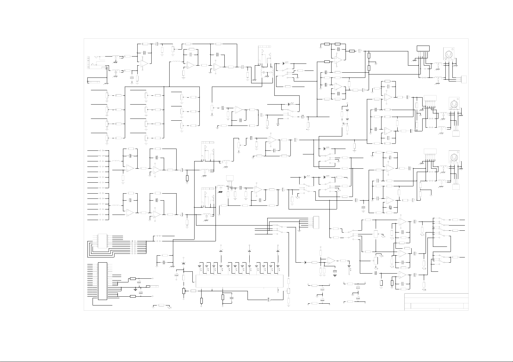
SUP3
1N
1
CON12
2
3
4
6
SUP4
5
1 2
1 2
1 2
1 2
1 2
1 2
1 2
1 2
1 2
1 2
1 2
1 2
1 2
1 2
CON7
14WAY
ROT
CON1
12
34
56
78
910
11 12
13 14
15 16
17 18
19 20
21 22
23 24
25 26
27 28
29 30
31 32
33 34
35 36
37 38
39 40
40WAY
IDCMH
LK20
LK21
LK9
LK10
LK11
LK12
LK22
LK23
LK24
LK25
LK1
LK2
LK3
LK4
1314
1112
CLEAN0V
910
78
56
34
12
2
1
2
1
2
1
2
1
1N
R13
3
VR3
15K
20KA
R14
3
VR4
15K
20KA
R15
3
VR5
15K
20KA
R16
3
VR6
15K
20KA
L1
0H
BUSREF
R43
100K
L2
0H
BUSREFBUS5
MATRIX
MTXL
MTXC
MTXR
MTX1
MTX2
MTX3
MTX4
MTX5
MTX6
MTX7
MTX8
MUTE 1
MUTE 2
MUTE 3
MUTE 4
ipcue
ipcuedc
OPCUE
OPCUEDC
sip
BUSREF
0V
0V
0V
48V
+18V
-18V
1/4JACKSL
2 PL2
1
1/4RPB
MWK CON
UNFITTED
MTX1 MTX5
MTX2
MTX3
MTX4
AUX1
AUX2
AUX3
AUX4
AUX5
AUX6
AUX7
AUX8
BUS1
BUS2
BUS3
BUS4
BUS6
bus8
bus7
BUS6
BUS5
BUS4
BUS3
BUS2
BUS1
MIXR
MIXC
MIXL
AUX8
AUX7
AUX6
AUX5
AUX4
AUX3
AUX2
AUX1
16V0.2
R4
5K1
C3
R5
100U
C2
R1
33P
V1-
10K
4
IC1A
2
3
MTX6
MTX7
MTX8
R44
10K
IC4B
NE5532
R67
4K7
IC7B
NE5532
LK13
1 2
3
5
7
9
11
13
15
16WAY
IDCVM
R113
1R
R114
1R
TL072
8
V1+
R3
5K1
R45
7
4K7
R68
7
4K7
4
6
8
10
12
14
16
C52
220U
25V
2 PL1
1
C53
220U
25V
R2
10K
C1
33P
C17
33P
6
5
C31
33P
6
5
100K
1
2
R17
3
VR7
15K
20KA
1
2
R18
3
VR8
15K
20KA
1
2
R19
3
VR9
15K
20KA
1
2
R20
3
VR10
15K
20KA
1
R46
10K
C18
33P
V-
4
IC4A
2
1
3
NE5532
8
V+
R69
10K
C32
33P
V-
4
IC7A
2
1
3
NE5532
8
V+
LK5
1 2
LK6
1 2
MATRIX
PRE/POST
LINKS
R110
100R
C61
10N
25V0.2
V+
1/4"RPB
V-
R115
0R
R6
2
4K7
R7
3
VR2
15K
20KA
C4
1
33P
L3
IC2B
6
0H
MTXL
MTXC
MTXR
R47
75R
R70
75R
POST
C56
22U
V-LED
500R
7
5
NE5532
R8
75R
2
R21
3
VR11
15K
20KA
1
2
R22
3
VR12
15K
20KA
1
2
R23
3
VR13
15K
20KA
1
C19
100U
16V0.2
R48
100K
100U
16V0.2
V+LED
PR2
V-LED
GROUP
INSERT
C33
R71
100K
LED12
RED
D1
18V
+12
R104
270K
1
V+
-21dB
ADJ
R105
10K
R10
10K
C5
33P
V-
4
R9
IC2A
10K
VR14
20KA
AUX
INSERT
CON11
1/4JACKSL
SUP11
1N
CON4
1/4JACKSL
SUP5
1N
2
3
213456
213456
R11
1
75R
NE5532
8
V+
C7
2
220N
3
5
1
6
R24
680K
R25
4K7
SUP12
1N
WIR3
3WAY
123
SUP6
1N
R153
240K
R154
27R
GRP/MTX METER
V+LED
D2
18V
LED9
LED11
5
D
1
2
I
2
YEL
LED10
YEL
R106
100K
LED8
YEL
YEL
6
D
1
1
1
7
8
0
D
D
D
1
9
8
0
I
T
/
/
P
C
3
4
R107
1M C58
V-LEDV-LED
16V0.2
C8
C34
220N
R72
7K5
LED7
GRN
1
1
D
7
C57
470N
C6
100U
R12
100K
IC1B
TL072
R26
7
75R
R27
33P
10K
C20
220N
2
3
VR1
10KA
1
FADER BUFFER
3
2
R73
680K
R74
4K7
V+LED
D3
18V
LED5
GRN
LED4
LED6
GRN
1
1
2
3
D
D
6
5
BA683A
SP2
V+
V-
MTXPK
POST
MTXPOST
GRN
D
4
IC12
1N
R50
4K7
8
4
1
4
CON3
1/4JACKSL
16V0.2
R49
680K
C35
33P
LED3
R28
100K
IC8A
NE5532
MTX AFL
LED16
213456
SP1
1N
MTXPK
LED15
C9
100U
V+
IC11A
8
TL072
3
1
2
4
C21
V-
33P
R76
1
75R
R75
10K
SW1
2PSUJ
V+LED
LED1
LED2
GRN
GRN
GRN
1
1
1
5
6
7
D
D
D
3
2
1
D
0
O
V
T
9
1
8
V-LED
2U2
63V0.2
YEL
SW4
2PSUJ
R156
10K
MTX CUT
LED15
RED
SW3
R51
75R
R52
10K
C36
220U
25V
D4
18V
-21
2PSUJ
OPCUE
C22
100U
16V0.2
LED17
R77
100K
R108
33K
PR1
5K
1/4V
R109
2K2
LED17
R157
OPCUEDC
47K
C10
100U
16V0.2
R29
100K
AUXMTR
CUT GROUP
LED17
RED
SW8
2PSUJ
NOT
NORMALY FITTED
AUXMTR
R100
56K
D5
R99
15K
1N4148
R101
47K
R111
V+
1R
R112
1R
V-
CON16
1
2
3
4
5
6
6WAY
MHLOPT
MTXPOST
AUX
V+
R30
10K
2
R33
3
10K
C12
220P
R37
10K
5
6
C13
100P
R41
10K
LED14
YEL
SW2
2PSUJ
LED18
YEL
SW9
2PSUJ
BUS PEAK
6
5
R102
2M2
V+LED
C54
22U
25V0.2
C55
22U
25V0.2
V-LED
AFL
IC11B
TL072
V1-
V1+
R125
BC212
AFL
R80
1K6
R81
1K
4
IC3A
8
R36
R38
IC3B
NE5532
R42
10K
150R
TR9
LED15
R152
1K5
7
C62
220N
R31
10K
C11
16V0.2
R32
100P
75R
1
NE5532
10K
10K
R39
20K
7
R40
C14
75R
100P
V+LED
D8
1N4148
D9
1N4148
R126
10K
V-LED
R55
100K
R53
47K
OPCUEDC
R54
10K
V-LED
R78
47K
R79
10K
POST
LCR
MODE
SW7
2PSUJ
R103
10K
LED13
RED
V-LED
R127
V+ V1+
10R
R128
10R
100U
16V0.2
OPCUE
C63
100U
16V0.2
C67
33P
FHVROP
CON9
C15
R34
3K6
R35
3K6
R56
10K
C23
R57
C16
100U
R82
1K6
R83
2K2
6
C59
22U
25V0.2
C60
22U
25V0.2
V1-V-
100P
V1-
10K
4
IC6A
2
R59
10K
C24
100P
R62
10K
C25
100P
R120
10K
R90
10K
R91
10K
C41
100P
R92
10K
C42
100P
R93
10K
2
CW
1
VR15A
5KB
X2NB
CW
5
VR15B
5KB
4
X2NB
C48
220N
R140
680K
LAST R
LAST C
LAST CON
LAST D
LAST LED
LAST IC
LAST SW
LAST VR
LAST LK
R58
1
3
75R
NE5532
8
V1+
R61
10K
R63
10K
IC6B
NE5532
5
7
6
C26
100P
R121
10K
R94
10K
C37
100P
V1-
4
2
1
3
IC10A
8
NE5532
V1+
R95
10K
R96
10K
IC10B
NE5532
5
7
6
C40
100P
R97
10K
3
2
R87
3 7
5K6
R84
R86
1M5
5
6
R88
C45
5K6
10P
5
6
R141
C49
5K6
10P
R157
C67
CON18
D7
LED17
IC12
SW9
VR15
LK25
6WAY
OPT XFMR
123456
1 2
1 2
C27
100U
16V0.2
R60
3K6
R65
3K6
R64
20K
C28
R66
75R
100U
16V0.2
C38
R98
75R
100U
16V0.2
R129
20K
C39
R147
75R
100U
16V0.2
PAN BUFFER
V+
IC9A
8
TL072
C46
1
100U
16V0.2
4
R138
V-
C44
100K
10P
3K6
R85
1M5
C47
7
100U
IC9B
16V0.2
TL072
R139
100K
R89
3K6
C50
7
100U
IC8B
16V0.2
NE5532
R143
100K
R142
4K7
Klark Teknik - DDA Division
Title
Size Document Number REV
C CD1286-1 A
Date: March 7, 1997 Sheet 1 of 1
LK16
LK17
FHVROP
CON2
6WAY
OPT XFMR
123456
LK18
1 2
LK19
1 2
FHVROP
CON10
6WAY
OPT XFMR
123456
LK7
1 2
LK8
1 2
R130
3K6
R131
3K6
CS8 - Group Matrix Output
MATRIX OUT
SUP9
1N 132
SUP10
1N
NOT NORMALY FITTED
AUX SEND
SUP13
1N
SUP14
1N
NOT NORMALY FITTED
GROUP OUT
SUP7
1N
SUP8
1N
NOT NORMALY FITTED
SW6
4PSUJ
CLEAN0V
SW5
2PSUJ
POST
CON5
NC3MAHL
CON8
NC3MAHL
CON6
NC3MAHL
4
R144
10K
CLEAN0V
R145
10K
R146
10K
CON13
3WAY
MH
1
2
3
4
132
CON14
123
3WAY
MH
4
132
CON15
3WAY
123
MH
MIXL
MIXR
MIXC

LEFT/MONO
1
CON2
2
3
SUP1
1N
4
6
5
1/4JACKSL
STEREO
INPUT
RIGHT
CON3
1/4JACKSL
MWK CONN
2 PL2
1
1/4RPB
UNFITTED
R116
910R
R117
6K2
PRE-L
PRE-R
R118
100K
V+LED
CON9
1
2
3
3WAY
NOT NORMALY FITTED
MH
BUS7
BUS8
MATRIX CONNECTOR
BUS8
BUS7
BUS6
BUS5
BUS4
BUS3
BUS2
BUS1
MIXR
MIXC
MIXL
AUX8
AUX7
AUX6
AUX5
Aux4
Aux3
Aux2
Aux1
C51
330N
1 2
1 2
CON7
14WAY
ROT
CON1
12
34
56
78
910
11 12
13 14
15 16
17 18
19 20
21 22
23 24
25 26
27 28
29 30
31 32
33 34
35 36
37 38
39 40
40WAY
IDCMH
1
2
3
4
6
5
LK1
LK2
CLEAN0V
SUP2
1N
IC13
5
4
7
6
9
8
11
10
LM2901
R119
820K
L2
BUSREF
1314
1112
910
78
56
34
12
MUTE 1
MUTE 2
MUTE 3
MUTE 4
IPCUE
IPCUEDC
OPCUE
OPCUEDC
sip
BUSREF
0V
0V
0V
48V
SUP3
1N
SUP4
1N R16
3
+
+
V
+
+
+
-
-
V
1
2
V-LED
C31
33P
0H
6
5
MTX7
MTX8
+18V
-18V
R1
10K
R2
10K
C1
33P
R15
10K
10K
C4
33P
O
O
O
O
D7
1 2
1 2
R55
C19
100P
C26
100P
GROUP
1
6
D
2
C58
2U2
63V0.2
V+
C21
IC4A
100U
8
TL072
16V0.2
3
1
2
4
R36
100K
C20
V-
R34
33P
10K
R43
R35
4K7
10K
R151
27R
6
R44
10K
IC4B
TL072
5
6
R40
10K
R41
4K7
R153
27R
AFL
LED17
YEL
SW12
2PSUJ
CUT
LED16
RED
SW10
2PSUJ
D4
18V
LED1
GRN
-21
1
7
D
1
R108
22K
0
V
PR1
9
5K
1/4V
V-LED
R109
2K2
10KB
CDNB
16V0.2 5
7
IC6B
C24
NE5532
100U
C28
POST-R
100U
16V0.2
7
R42
100K
C27
33P
LED18
R78
47K
R79
10K
POST
R80
1K6
R81
1K
CON10
1
2
3
3WAY
MH
D8
1N4148
D9
1N4148
R126
10K
V-LED
POST-L
R45
100K
R46
6K8
VR4
3
R49
6K8
16V0.2
OPCUEDC
OPCUE
100U
LCR
MODE
R125
150R
BC212
V+
C23
100U
84IC5A
16V0.2
3
NE5532
1
2
2
1
R132
100K
C22
V-
33P
R47
10K
R48
7K5
POST-M
BALANCE
C30
IC5B
100U
NE5532
16V0.2
5
7
6
R51
7K5
C43
C68
33P
SW9
2PSUJ
V+LED
TR9
LED14
C29
33P
R50
10K
R90
10K
2
R91
3
10K
C41
100P
R92
10K
5
6
C42
100P
R93
10K
PAN BUFFER
R82
1K6
R83
2K2
6
R133
100K
R94
10K
C37
100P
V1-
4
IC10A
8
NE5532
V1+
R95
10K
R96
10K
IC10B
NE5532
C40
100P
R97
10K
2
CW
3 7
1
VR9A
5KB
X2NB
CW
5
VR9B
5KB
4
X2NB
C48
220N
R140
680K
LAST R
LAST C
LAST CON
LAST D
LAST LED
LAST IC
LAST SW
LAST VR
LAST LK
MIX
R52
SW2
10K
R53
10K
2PSUJ
MONO
R54
SW3
10K
2PSUJ
CLEAN0V
PRE
SW1
POST-M
PRE-M
POST-R
PRE-R
POST-L
PRE-L
STEREO
C38
R98
1
75R
100U
16V0.2
R129
20K
C39
R147
7
75R
100U
16V0.2
V+
3
2
V-
C44
R87
33P
5K6
R84 3K6
R85
R86
1M5
5
6
C45
R88
5K6
33P
5
6
R141
C49
5K6
33P
R148
C68
CON10
D9
LED20
IC13
SW15
VR9
LK8
CLEAN0V
2
4PSUJ
1
2
1
SW13
2PSUJ
FHVROP
CON5
6WAY
OPT XFMR
123456
LK7
R130
1 2
3K6
LK8
1 2
R131
3K6
CLEAN0V
IC9A
8
TL072
C46
1
100U
16V0.2
4
R138
100K
1M5
C47
TL072
7
100U
IC9B
16V0.2
R139
100K
R89
3K6
IC8B
NE5532
C50
7
100U
16V0.2
R143
100K
R142
4K7
DDA, HOUNSLOW, MIDDX, TW3 2EB, ENGLAND.
Title
Size Document Number REV
C CD1280-1 A
Date: March 7, 1997 Sheet 1 of 1
VR2A
2
3
6
5
C54
22U
25V0.2
C55
22U
25V0.2
1 2
33P
4 5
33P
V+LED
V-LED
R7
1K6
R6
1K5
C7
V-
4
IC2A
1
R9
TL072
8
1K8
V+
R148
3K
R28
100K
R21
1K5
C14
R29
100K
IC2B
7
TL072
R22
1K6
LED18
GRN
LED19
YEL
R24
1K8
R149
3K
LED20
CON4
RED
1/4JACKSL
SUP5
1N
R110
100R
C61
10N
C56
22U
25V0.2
V-LED
R3
3K3
C3
C2
100U
16V0.2
33P
V-
4
IC1A
2
1
R13
3
100K
TL072
8
V+
R4
3K3
R18
3K3
C6
100U
C5
16V0.2
33P
IC1B
6
7
R19
5
100K
TL072
R17
3K3
LED18
V+LED
R120
R121
10K
10K
2
1
14
13
D6
1N4148
1N4148
R67
4K7
IC7B
7
NE5532
LK3
LK4
R113
1R
R114
1R
V+LED
R122
22K
8
3
2
IC11A
4
TL072
R123
68K
V-LED
R69
10K
C32
33P
V-
R68
4
IC7A
2
4K7
3
NE5532
8
V+
LK5
1 2
LK6
1 2
MATRIX
PRE/POST
LINKS
V+
C52
220U
25V
2 PL1
1
1/4"RPB
C53
220U
25V
V-
0R
VR1A
R5
10KB
820R
3
R136
3K9
VR1B
10KB
R20
820R
6
R137
3K9
SIG
0dB
TR8
R124
1
100K
BC212
PEAK
R157
2K2
V-LED
C33
100U
R70
16V0.2
1
75R
R71
100K
POST
V+
R111
1R
R112
V-
1RR115
R8
10KB
1 2
1K6
C10
3
C9
33P
2N2
V-
4
IC3A
2
1
3
R10
TL072
8
22K
V+
3
R12
1 2
1K8
VR3A
10KB
C11
C67
470N
470N
V+
100U
8
16V0.2
3
1
2
C13
4
IC6A
V-
NE5532
VR2B
10KB
R23
4 5
1K6
6
C15
C63
2N2
10P
IC3B
6
7
5
R26
TL072
22K
6
R25
4 5
1K8
VR3B
10KB
C16
C64
470N
470N
D5
1N4148
GROUP
INSERT
213456
SUP6
1N
R154
240K
R155
27R
V+LED
LED12
D1
18V
+12
R104
270K
1
V+
-21dB
ADJ
PR2
500R
R105
10K
V-LED
CUT
LED14
LED14
RED
PRE-L
R14
100K
PRE-R
V+LED
R100
56K
R101
47K
FADER BUFFER
C34
220N
R73
680K
R72
7K5
R74
4K7
V+LED
LED9
YEL
LED10
YEL
7
8
D
D
1
9
0
I
T
/
/
P
C
3
4
R107
1M
V-LEDV-LED
SW14
4PSUJ
PFL
LED15
YEL
SW8
4PSUJ
BUS PEAK
6
5
R102
2M2
V+
8
3
2
4
C35
V-
D2
18V
LED8
YEL
1
0
D
8
IC11B
LED7
TL072
IC8A
NE5532
33P
GRN
LED16
7
C62
220N
1
1
1
D
7
C57
470N
C12
100U
16V0.2
PRE-M
R30
100K
C17
100U
16V0.2
R27
100K
R99
15K
WIR3
3WAY
123
LED11
RED
YEL
5
6
D
D
1
1
2
1
I
2
R106
100K
C18
220N
WIR1
3WAY
R31
123
7K5
R150
240K
C65
100P
WIR2
3WAY
123
C25
220N
R37
7K5
R11
10K
IPCUE
R135
IPCUEDC
47K
R103
10K
LED13
RED
V-LED
C36
R76
220U
75R
25V
R77
100K
R75
10K
V+LED V+LED
D3
18V
LED5
GRN
LED3
LED4
LED6
GRN
GRN
1
1
1
2
3
4
D
D
D
6
5
4
BA683A
R33
1K
R32
680K
R39
1K
R38
680K
R152
240K
C66
100P
LED16
LED2
GRN
GRN
1
5
D
3
D
O
T
1
8IC12
MIXL
MIXR
MIXC
R63
10K
3
AUX5 AUX6
VR5
20KA
R65
10K
3
AUX7 AUX8
VR7
20KA
GROUP OUT
SUP7
1N
SUP8
1N
POST
CS8 GROUP/FX OUTPUT
SW4
10K
1-2
R56
10K
2PSUJ
R57
SW5
10K
3-4
R58
10K
2PSUJ
SW6
R59
10K
5-6
R60
2PSUJ
10K
R61
SW7
10K
7-8
R62
2PSUJ
10K
2
R64
10K
3
VR6
1
20KA
2
R66
10K
3
VR8
1
20KA
CON6
NC3MAHL
4
132
NOT NORMALY FITTED
V+ V1+
R127
10R
R128
10R
MIX
R144
10K
R145
10K
SW11
4PSUJ
MONO
SW15
R146
10K
2PSUJ
C59
22U
25V0.2
C60
22U
25V0.2
BUS1
BUS2
BUS3
BUS4
BUS5
BUS6
BUS7
BUS8
CON8
1
2
3
3WAY
MH
V1-V-
MIXL
MIXR
MIXC

AUX1
L1
AUX1
0H
BUSREF
R1
22R
LEFT
MIX
L2
MIXL
0H
BUSREF
BUSREF
RIGHT
MIX
L3
MIXR
0H
BUSREF
bus8
bus7
bus6
MATRIX CONNECTOR
R2
10K
C1
33P 0.2
V-
4
IC1A
2
1
3
NE5532
8
V+
R26
4K7
C11
33P 0.2
V-
4
IC4A
2
1
3
NE5532
8
V+
REC-C
R32
4K7
C14
33P 0.2
V-
4
IC5A
2
1
3
NE5532
8
V+
CON16
1314
1112
910
78
56
34
12
14WAY
ROT R87
R4
10K
C2
33P 0.2
R3
IC1B
6
7
5
4K7
NE5532
R28
10K
C12
33P 0.2
R27
IC4B
6
4K7
5
NE5532
IC2B
TL072
5
6
R169
100K
R34
10K
C15
33P 0.2
R33
IC5B
6
4K7
5
NE5532
LPOST
CPOST
RPOSTREC-C
bus1
bus2
bus3
bus4bus5
CON4
1/4JACKSL
AUX
INSERT
C4
220N
SP2
1N
213456
2
3
16V0.2
CON5
1/4JACKSL
100U
100U
CON6
1/4JACKSL
C74
R31
C75
1K
DUALPHONO
R86
100R
C37
10N
VR1
10KA
1
LEFT
INSERT
213456
R160
100K
CON2
TAPE
R37
RECORD
1K
-10dBV
RIGHT
INSERT
213456
SP1
C3
100U
16V0.2
R6
10K
SP3
1N
R162
1K5
R163
1K5
SP5
1N
16V0.2
V+ V+
10K
V-
1N
C13
100U
16V0.2
R30
1K5
16V0.2
R36
1K5
C16
100U
R161
100K
R11
150R
TR17
BC212
LED14
R5
75R
R29
7
75R
SP13
1N
7
R35
7
75R
D16
1N4148
D17
1N4148
V+
IC2A
8
TL072
3
2
R7
680K
R10
4K7
WIR1
3WAY
SP4
1N
R142
WIR2
3WAY
SP6
1N
R143
R8
1
75R
4
C5
V-
R9
33P 0.2
10K
AFL
LED14
YEL
SW1
LED14
123
C17
220N
R124
1K
C38
R38
7K5
680K
220P
R42
LFDR
9K1
16V0.2
R172
240K
R49
56K
D11
R48
15K
1N4148
R50
47K
123
C21
220N
R120
1K
C39
R43
7K5
680K
220P
R47
RFDR
9K1
16V0.2
R171
240K
R54
56K
D12
R53
15K
1N4148
R55
47K
C6
100U
16V0.2
2PSUJ
10K
R13
FADER BUFFER
V+
8
3
2
4
C18
V-
C20
33P 0.2
100U
R41
10K
V+
BUS PEAK
V-
4
2
3
8
V+
R51
2M2
FADER BUFFER
5
6
C22
C24
33P 0.2
100U
R46
10K
R170
V+
68R
BUS PEAK
6
5
R56
2M2
IC7A
IC7B
R12
47K
IC6A
NE5532
R173
68R
TL072
IC6B
NE5532
TL072
AUXMTR
LED15
1
1
7
7
OPCUEDC
OPCUE
C35
220N
C36
220N
C64
220P
C65
220P
R39
C19
75R
100U
16V0.2
R149
100K R150
R40
10K
R52
10K
LED13
RED
V-
R44
C23
75R
100U
16V0.2
R151
100K
R45
10K
R57
RPEAK
10K
R14
10K
V1-
4
2
R15
3
8
10K
V1+
R19
R16
R20
10K
IC3B
NE5532
5
6
R17
R21
10K
10K
RIGHT
LED23
R82
V+ V1+
10R
R83
10R
R18
C7
220P
IC3A
NE5532
C8
220P
CUT
10K
1
10K
10K
7
LEFT
CUT
LED22
RED
LED23
RED
SW10
2PSUJ
SW9
2PSUJ
C33
22U
25V0.2
C34
22U
25V0.2
R22
75R
R153
20K
R23
75R
LED23LED22
LED24
R152
100K
V1-V-
C9
100U
16V0.2
C10
100U
16V0.2
C72
100U
16V0.2
100K
C73
100U
16V0.2
USE WITH PC 1396
SEE ALSO CD1282-1
FHV
CON13
6WAY
123456
LK1
1 2
R24
3K6
LK2
1 2
R25
3K6
R62
R58
10K
10K
C25
220P
V1-
4
2
1
R59
3
IC8A
8
NE5532
10K
C66
V1+
220P
R63
10K
R60
R64
10K
10K
IC8B
NE5532
5
7
6
C67
220P
C26
220P
R61
R65
10K
10K
LPOST
RPOST
R74
R70
10K
10K
C29
220P
V1-
4
2
R71
1
3
IC9A
NE5532
10K
8
C68
V1+
220P
R75
10K
R72
R76
10K
10K
IC9B
NE5532
5
7
6
C69
220P
C30
220P
R73
R77
10K
10K
SP7
1N
SP8
1N
R66
75R
R154
20K
R67
75R
R78
75R
R155
20K
R79
75R
LAST R
LAST C
LAST CON
LAST D
LAST LED
LAST IC
LAST SW
LAST VR VR3
LAST TR
16V0.2
16V0.2
C27
100U
C28
100U
16V0.2
C31
100U
C32
100U
16V0.2
CON7
NC3MAHL
4
AUX SEND
132
CON18
1
2
3
3WAY
MH
NOT NORMALY FITTED
LEFT MIX OUT
FHV
CON14
6WAY
123456
LK3
1 2
R68
R197
C86
CON24
D21
LED24
IC14
SW12
TR21
3K6
R69
3K6
R80
3K6
R81
3K6
LK4
1 2
LED18
LED22
GRN
FHV
CON15
6WAY
123456
LK5
1 2
LK6
1 2
RIGHT MIX OUT
DDA, HOUNSLOW, MIDDX, TW3 2EB, ENGLAND.
Title
CS8 MASTER MODULE.
Size Document Number REV
C CD1281-1 A
Date: February 27, 1997 Sheet 1 of 2
SW8
4PSUJ
SP9
SP10
SP11
SP12
MWKGND
1N
1N
1N
1N
V+
V+
V-
V-
GND
CON8
NC3MAHL
LED18
L+R TO C
R84
15K
R85
15K
LPOST
RPOST
CON9
NC3MAHL
NOT NORMALY FITTED
4
132
CON19
1
2
3
3WAY
MH
MIXC
4
132
CON20
1
2
3
3WAY
MH

CON10
1
2
3
4
5
6
7
8
9
10
11
12
12WAY
MHR/A
LINK TO COMMS PCB
CPOST
CPOST
LPOST
LPOST
RPOST
RPOST
NOT
NORMALLY
FITTED
CON21
1
2
3
4
5
6
6WAY
MHLOPT
IPCUE
OPCUE
D20
D21
C86
220N
V-
SIP
V+ V+LED
R130
1R
R131
V- V-LED
1R
R98
47K
C43
V-
33P
2
R97
3
VR2A
10KA
SW4
4PSUJ
X2NB
VR2B
10KA
X2NB
CPOST
L4
0H
6
5
D5
C54
470N
V-
V+
V+
R139
TR14
BC212
100K
R138
100K
RPEAK
LTAPE
RTAPE
LMON
RMON
CPRE
METEROFF
RPEAK
RPOST
CFDRLEFT
CFDRRIGHT
CMON
+48VPRE
MIX
TO
MON
AUXMTR
TR6
J111
TR21
J175
R196
1M
R197
68K
V+
R140
100K
C85
100N
TR15
BC182
22K
1
5
R100
6
22K
4
TAPE
SW6
4PSUJ
R108
SOLOMTR
4K7
C51
33P
R109
7
IC11B
4K7
NE5532
V+
R135
100K
R117
100K
R137
4K7
R136
100K
2
3
6
5
2
3
V+
R90
47K
SOLO
SOLO
IN
PLACE
LED15
LED15
RED
0.2
4
IC13A
1
TL072
8
C45
33P
0.2
IC13B
7
TL072
C TO MON L/R
LEVEL
R110
3
4K7
R111
33K
C52
33P
V-
4
IC11A
1
NE5532
8
V+
IPCUEDC
SW7
2PSUJ
C44
1000U
6.3V
C46
1000U
6.3V
R101
10K
SW5
2PSUJ
2
1
INPUT CUE
OUTPUT CUE
C60
22U
25V0.2
C61
22U
25V0.2
OPCUEDC
C57
2U2
63V0.2
R99
10K
VR3
10KB
CDNB
100U
16V0.2
TAPETO
L/R
SW2
LFDR
RFDR
2PSUJ
TAPETO
CENTRE
SW3
R164
10K
BC182
BC182
INPUT
CUE
TR10
LED18
TR8
R168
10K
LED16
YEL
D7
D8 R126
LED17
YEL
2PSUJ
R102
15K
R103
15K
R104
10K
R105
10K
R166
10K
R167
10K
R112
10K
R113
10K
R114
C53
10K
R115
10K
V+
R118
4K7
R119
TR7
47K
BC182
R116
220K
V-
V-
V+
R122
47K
C58
10N
R123
47K
TR9
OUTPUT
BC182
R121
220K
V-V-
CUE
V-
CENTRE CUT
LED24
V- SW12
MIXDC
D9
R128
100K
V+
RED
CPRE
TR18
J111
2
3
TR19
J111
TR1
6
J111
5
TR2
J111
TR3
J111
TR4
2
J111
3
SOLODC
C70
C71
100N
100N
V-
R127
47K
R125
C59
10K
10N
150K
2PSUJ
R165
10K
V-
4
8
V+
R106
10K
C47
33P
R107
10K
C49
33P
V-
4
IC12A
8
TL072
V+
V-
V+
TR11
BC182
V-
LED24
C76
33P
1
IC14A
TL072
7
IC12B
TL072
1
D10
R129
100K
* FOR METER BRIDGE OPTIONS
REMOVE LK9 AND FIT R190
R156
WW-4W
CPOST
6
5
C77
100U
16V0.2
C48
100U
16V0.2
C50
100U
16V0.2
22R
-18V +18V
CMON
LMON
RMON
1 2
*
R176
R188
10K
10K
C81
220P
V1-
4
2
C78
R189
100U
10K
16V0.2
R187
100K
7
IC14B
TL072
C41
22U
25V0.2
LPOST
SOLOMTR
D14
R144
100K
METEROFF
LK9
CON11
1
2
LITTLITE
3
3WAY
MH
R157
22R
WW-4W
C79
220P
R174
10K
C80
220P
R175
10K
V+LED
D1
18V
R91
270K
500R
PR2
V-
V-LED
D15
R145
100K
R190
100KOPT
*
R95
33K
R134
12K
1
-21dB
ADJ
R92
10K
EXT METER POWER
NOT NORMALY FITTED
V-LED
TR12
J111
TR13
J111
R180
1
3
75R
IC15A
8
NE5532
V1+
R177
10K
R178
10K
IC15B
NE5532
5
7
6
C82
220P
R179
10K
LED12
LED11
RED
YEL
+12
5
6
D
D
1
1
2
1
V+
I
2
R93
100K
V-LED
PR1
5K
C40
1/4V
2U2
63V0.2
R96
2K2
clean0v
MWKGND
R193
1R5
TR20
R194
ZTX553
100K
R195
33K
C55
33U
63V
C83
100U
16V0.2
R181
20K
C84
R182
75R
100U
16V0.2
V+LED V+LED
D2
18V
LED9
YEL
LED8
LED10
YEL
YEL
1
7
8
0
D
D
D
1
9
8
0
I
T
/
/
P
C
3
4
R94
1M
V-LED
bus8
bus7
bus6
bus5
bus4
bus3
bus2
bus1
MIXR
MIXL
aux8
aux7
aux6
aux5
aux4
aux3
aux2
aux1
AUX1
+48VPRE
D18
R88
4K7
SW11
2PSUJ
CON24
1
2
3
3WAY
MH156
LAST R
LAST C
LAST CON
LAST D
LAST LED
LAST IC
LAST SW
LAST VR
LAST TR
FHV
CON17
6WAY
123456
SP15
1N
LK7
1 2
R183
3K6
LK8
1 2
SP14
R185
3K6
CENTRE MIX OUT
LED5
GRN
LED6
LED7
GRN
GRN
1
1
1
1
2
3
D
D
D
7
6
5
C42
470N
CON1
MUTE1
12
MUTE2
34
MUTE3
56
MUTE4
78
IPCUE
910
IPCUEDC
11 12
OPCUE
13 14
OPCUEDC
15 16
SIP
17 18
BUSREF
19 20
21 22
23 24
25 26
0V
27 28
0V
29 30
0V
31 32
33 34
35 36
37 38
39 40
40WAY
IDCMH
2 PL2
1
+48V
TR16
TIP32C
VERT
R191
2K7
R192
2K7
+18V
-18V
R197
C86
CON24
D21
Title
LED25
IC14
Size Document Number REV
SW12
VR3
C CD1282-1 A
TR21
Date: March 6, 1997 Sheet 2 of 2
1N
D3
18V
LED3
LED4
LED2
GRN
GRN
GRN
1
1
1
4
5
6
D
D
D
4
3
2
D
O
T
1
8
LEFT METER
OPCUE
OPCUEDC
BUSREFMIXC
GND
MWK CON
+48V
UNFITTED
R186
1/4"RPB
27K
R146
27K
R147
10K
R148
10K
USE WITH PC1396-1
SEE ALSO CD1281-1
DDA, HOUNSLOW, MIDDX, TW3 2EB, ENGLAND.
CS8 MASTER MODULE.
V+LED
V-LED
D
1
0
V
+18V
-18V
CON23
NC3MAHL
NOT NORMALY FITTED
D4
18V
LED1
GRN
-21
1
7
IC10
BA683A
9
R132
1R
220U
R133
1R
LED25
GRN
LED19
RED
LED20
GRN
LED21
GRN
CON12
1
2
3
4
5
6
6WAY
MH156
4
132
C62
2 PL1
25V
1
C63
220U
25V
POWER IN
V+
V-
1/4"RPB
CON22
3WAY
MH
1
2
3
V+
V-
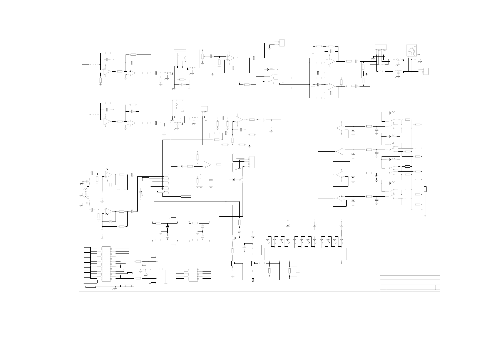
AUX2
AUX2
CENTRE
MIX
MIXC
SP5
1N
CON9
DUALPHONO
16V0.2
BUS8
BUS7
BUS6
BUS5
BUS4
BUS3
BUS2
BUS1
MIXR
MIXC
MIXL
AUX8
AUX7
AUX6
AUX5
AUX4
AUX3
AUX2
AUX1
CLEAN 0V
MWKGND
16V0.2
BUSREF
BUSREF
C14
100U
100U
MIXC
AUX2
CON23
1
2
AUX METER
AUX
CON4
SP1
1N
REC-C
R30
CON11
12WAY
1
2
3
4
5
6
7
8
9
10
11
CMON
12
METEROFF
RPOST
C36
22U
25V0.2
C37
22U
25V0.2
V+
V-
1/4JACKSL
SP2
1N213456
R74
100R
C38
10N
CON5
1/4JACKSL
SP3
213456
1N
SP4
1N
CFDRLEFT
CFDRRIGHT
V1+
R32
56K
R31
D5
MHR/A
15K
R33
47K
+48VPRE
V1+
V1+ V+ V+LED
V1- V- V-LED
V1-
MATRIX CONNECTOR
REC-C
bus8
bus7
bus6
R76
1R C34
R77
1R
CON20
1314
1112
910
78
56
34
12
14WAY
ROT
2
220N
3
VR1
10KA
1
WIR1
3WAY
123
BUS PEAK
IC2B
6
5
R34
2M2
22U
25V0.2
C35
22U
25V0.2
lpost
CPOST
rpost
bus1
bus2
bus3
bus4bus5
C4
TL072
V1+
IC2A
8
TL072
3
1
2
R7
R36
18K
R37
18K
C24
220N
R10
4K7
C17
220N
R38
680K
R35
10K
R186
100K
CPOST
4
C5
V1-
33P
FADER BUFFER
3
2
C20
100U
16V0.2
R300
240K
V+LED
CPEAK
V-LED
D14
1N4148
TR6
J111
R51
33K
PR1
5K
1/4V
V+LED
V+
V-
R41
10K
V-
25V0.2
R52
2K2
680K
R184
7K5
7
C6
R8
100U
75R
16V0.2
R9
10K
R314
5K6
IC6A
8
NE5532
R39
1
4
C18
33P
R301
68R
TR5
J111
R185
100K
D15
1N4148
C29
22U
V-LED
C19
75R
100U
16V0.2
R40
10K
CON3
6
5
4
3
2
1
6WAY
FHV
V+LED
LED12
D1
18V
+12
R53
270K
1
-21dB
ADJ
PR2
500R
1/4V
R54
10K
V-LED
C30
2U2
50VLP
V-
RIGHT
PEAK
1R
INSERT
R5
C3
75R
100U
16V0.2
R6
100K
CENTRE
INSERT
C13
R29
100U
75R
16V0.2
100K
LMON
RMON
CPRE
LED13
RED
V+
R72
10R
R73
V-
10R
V+
C32
220U
25V
2 PL1
1
1/4"RPB
C33
220U
25V
V-
R2
10K
C1
10P
L1
V-
0H
4
IC1A
2
1
3
NE5532
8
V+
R1
100K
R26
4K7
C11
10P
L2
V-
0H
4
IC4A
2
1
3
NE5532
8
V+
TAPE BUFFER
V1+
IC5A
8
NE5532
3
1
2
4
R43
47K
C15
V1-
33P
R46
10K
SP6
1N
C21
IC5B
NE5532
5
7
6
R47
47K
C22
33P
R50
10K
TAPE BUFFER
CON1
12
34
56
78
910
11 12
13 14
15 16
17 18
19 20
21 22
23 24
25 26
27 28
29 30
31 32
33 34
35 36
37 38
39 40
40WAY
IDCMH
0V
0V
0V
R3
4K7
R27
4K7
R44
75R
R45
9K1
R48
75R
R49
9K1
ipcue
ipcuedc
OPCUE
OPCUEDC
sip
BUSREF
+48V
MUTE1
MUTE2
MUTE3
MUTE4
2 PL2
1
R4
10K
C2
10P
IC1B
6
7
5
NE5532
R28
10K
C12
10P
IC4B
6
7
5
NE5532
C16
100U
16V0.2
C23
100U
16V0.2
R70
1R
+18V
GND
R71
-18V
MWK CON
1/4RPB
UNFITTED
3
3WAY
MH
AFL
LED14
LED15
YEL
SW1
2PSUJ
R189
100K
RED
5
D
1
2
V+
I
2
V-LED
R12
OPCUEDC
47K
OPCUE
10K
R13
CPRE
V+LED
D2
18V
LED9
LED11
YEL
LED10
LED8
YEL
YEL
6
D
D
1
1
0
1
I
/
P
3
R55
100K
LED7
YEL
GRN
1
0
8
7
D
D
8
9
T
/
C
4
R56
1M
V-LED
220P
220P
V+LED V+LED
LED5
GRN
LED6
GRN
1
1
1
3
2
1
D
D
D
5
6
7
RIGHT METER
C31
470N
R14
10K
10K
C7
220P
V1-
4
2
R15
10K
C65
R16
10K
C66
R17
10K
MUTE1
MUTE2
MUTE3
MUTE4
D3
18V
LED4
1
3
IC3A
8
NE5532
V1+
R19
10K
R20
10K
IC3B
NE5532
5
7
6
C8
220P
R21
10K
NE5532
1
7
1
NE5532
7
LED2
LED3
GRN
GRN
GRN
1
1
1
6
5
4
D
D
D
2
3
4
D
O
T
1
8
V-LED
C9
R22
75R
100U
16V0.2
R222
20K
C10
R23
75R
100U
16V0.2
V+
IC18A
8
3
2
D22
5V1
4
V-
IC18BNE5532
5
6
D23
5V1
V+
IC19ANE5532
8
3
2
D20
5V1
4
V-
IC19B
5
6
D21
5V1
D4
18V
LED1
GRN
-21
1
7
IC9
D
BA683A
1
0
V
9
LAST R
LAST C
LAST CON
LAST D
LAST LED
LAST IC
LAST SW
LAST VR VR4
LAST TR
CON18
6WAY
FHVR18
123456
SP7
1N
LK2
1 2
R24
3K6
LK3
1 2
SP8
R25
3K6
LED15
R310
100K
R311
100K
R312
100K
R313
100K
R314
C106
CON23
D21
LED18
IC19
SW14
TR6
1N
AUX 2 SEND
LED15
RED
SW2
C102
470N
2PSUJ
LED16
RED
SW3
C103
470N
2PSUJ
LED17
RED
SW4
C104
470N
2PSUJ
LED18
RED
SW5
C105
470N
2PSUJ
USE WITH PC1397-1
SEE ALSO CD1284-1
DDA, HOUNSLOW, MIDDX, TW3 2EB, ENGLAND.
Title
CS8 COMMS MASTER (CENTRE MIX)
Size Document Number REV
C CD1283-1 A
Date: February 5, 1997 Sheet 1 of 2
R214
330K
R302
100K
R304
330K
R216
100K
R306
330K
R229
100K
R308
330K
R220
100K
CON7
NC3MAHL
4
132
CON22
1
2
3
3WAY
MH
R215
100K
R303
220K
R218
100K
R305
220K
R219
100K
R307
220K
R11
75R
R221
100K
R309
220K
V+V-
V-LED

V+
R78
100K
C39
2U2
63V0.2
D16
9V1
C53
100N
C54
100N
R95
150R
CON14
NC3FAHR
231
SP11
1N
R79
100K
R80
10K
C40
2U2
63V0.2
D17
R81
9V1
10K
V+
8
IC16A
3
1
2
TL072
4
V- R97
18K
R96
9K1
TALKBACK
MIC
LINK FOR +48V
PHANTOM POWER
4
R104
C55
680P
C56
680P
SP12
1N R107
6K8
0.2
0.2
C42 10P
V1-
2
3
V1+
C41
10P
0.2
R98
6K2
0.2
R82
150K
4
1
IC7A
8
NE5532
R99
10K
1 2
R105
6K8
R106
10R
10R
C43
470N
R83
100K
IC16B
5
7
6
TL072
D18
D19
OSCILLATOR
LK1
LK03-OPT
C57
33U
63V0.2
R108
2K2
C58
33U
63V0.2
R86
R88
1K5
C106
100N
C46
470N
R103
820R
2PSUJ
PINK/1KHz
R89
C50
470N
100K
R90
330R
1K2
C47
C48
100N
220N
OSC ON
SW6
SW7
4PSUJ
3K3
R87
IC7B
R230
NE5532
100K
5
6
R100
10K
+48VPRE
150K
C44 10P
R84
10K
11K
7
C45
470N
R85
0.2
C96
2U2
63V0.2
R101
3K9
R102
820R
TALKBACK
R112
R109
R110
D10
9V1
10K
D11
9V1
R111
24K
D12
9V1
D13
9V1
10K
V+
33R
IC15
7
1
8
3
2 6 5
C59
220P
SSM2017
0.2
4
V-
IC6B
5
7
6
C52
R94
NE5532
R93
150K
100U
100K
16V0.2
0.2
VR2
2
20KA
3
1
SW8
470R
R114
470R
R115
470R
R116
4PSUJ
R163
VR4A
LMON
CMON
RMON
10KAX3
4K7
2
3
1
MONITOR
VOLUME MONITOR
R167
VR4B
10KAX3
4K7
5
6
4
R171
4K7
R117
R118
VR4C
8
9
7
10KAX3
R119
4K7
47K
2
3
R164
33K
R168
33K
R172
33K
C62 10P
V-
V+
R91
C49
47N
C51 10P
R92
10K
VR3
2
10KRD
3
1
C60
1000U
6.3V
C61
100U
16V0.2
R113
100K
TALKBACK
MONITOR
LEFT
R165
100K
C72 10P
0.2
C73
100U
IC11B
6
5
C74 10P
2
3
C76 10P
6
5
47K
0.2
4
IC10A
1
TL072
8
16V0.2
7
TL072
R166
100K
100K
CENTRE
R169
0.2
V-
4
IC11A
C75
1
TL072
100U
16V0.2
8
V+
R173
100K
0.2
IC10B
C77
7
TL072
100U
16V0.2
MONITOR
RIGHT
C63
100U
16V0.2
R120
100K
PHONES
ON
SW14
R170
100K
6PSUJ
R174
100K
C78
220P
0.2
C84
220P
0.2
R179
R175
10K
10K
C80
220P
LEFT MONITOR
V1-
0.2
4
2
R176
3
10K
V1+
R180
R177
R181
10K
5
6
C79
220P
0.2
R178
R182
10K
10K
R188
10K
V1-
2
R227
3
10K
V1+
R193
R228
R194
10K
5
6
C85
220P
0.2
R191
R195
10K
10K
1
IC12A
8
NE5532
10K
10K
IC12B
NE5532
7
C81
220P
0.2
R192
10K
C86
220P
CENTRE MONITOR
0.2
4
1
IC14A
8
NE5532
10K
10K
IC14B
NE5532
7
C87
220P
0.2
R224
75R
100U
16V0.2
R183
20K
C83
R225
75R
100U
16V0.2
C88
R197
75R
100U
16V0.2
R196
20K
C89
R198
75R
100U
16V0.2
CON15
NC3MAHL
4
132
SP13
1NC82
R226
3K6
R187
3K6
SP14
1N
CON21
NC3MAHL
4
132
SP17
1N
R199
3K6
R200
3K6
SP18
1N
SW9
2PSUJ
SW10
2PSUJ
SW11
2PSUJ
SW12
2PSUJ
AUX1-3
10K
R121
AUX1
10K
R122
AUX2
10K
R123
AUX3
AUX4-6
10K
R124
AUX4
10K
R125
AUX5
10K
R126
AUX6
AUX7-8
10K
R127
AUX7
10K
R128
AUX8
MIX
10K
R129
MIXL
10K
R130
MIXR
10K
R131
MIXC
SW13
2PSUJ
+48V
+48V
V+
V+
V-
VV1+
V1+
V1-
V1-
MWKGND
GND
BUS
10K
R132
BUS1
10K
R133
BUS2
10K
R134
BUS3
10K
R135
BUS4
10K
R136
BUS5
10K
R137
BUS6
10K
R138
BUS7
10K
R139
BUS8
V+
R140
47R
R141
47R
V-
V2+
C64
1000U
R142
25V
0R
C97
1000U
25V
V2-
C98
220N
R143
220K
C69
220N
R153
220K
V2+
D6
8
IC17A
3
1
2
R144
680K
R145
3K3
5
6
R154
680K
R155
3K3
D7
TL072
4
C99
V2-
33P
0.2
R146
10K
D8
IC17B
7
D9
TL072
C70
33P
0.2
R156
10K
V2+
TR1
R147
BC182
10K
R148
10K
R157
10K
R158
10K
R149
220U 25V
220U 25V
C71
R152
75R
C100
R151
10K
R162
75R
R161
10K
USE WITH PC1397-1
SEE ALSO CD1283-1
PHONES
CON17
3
2
1
3WAY
MH
C90
220P
0.2
LAST R
LAST C
LAST CON
LAST D
LAST LED
LAST IC
LAST SW
LAST VR VR4
LAST TR
33R
R150
33R
TR2
BC212
V2-
V2+
TR3
BC182
R159
33R
R160
33R
TR4
BC212
V2-
R205
R201
10K
10K
C92
RIGHT MONITOR
220P
V1-
0.2
4
2
R202
1
3
IC13A
10K
8
NE5532
V1+
R206
10K
R203
R207
10K
10K
IC13B
NE5532
5
7
6
C91
220P
0.2
C93
220P
R204
0.2
R208
10K
10K
R314
C106
CON22
D19
LED18
IC17
SW14
TR6
C94
R210
75R
100U
16V0.2
R209
20K
C95
R211
75R
100U
16V0.2
DDA, HOUNSLOW, MIDDX, TW3 2EB, ENGLAND.
Title
CS8 COMMS MASTER (TB/MONITOR)
Size Document Number REV
C CD1284-1 A
Date: March 14, 1997 Sheet 2 of 2
CON16
NC3MAHL
4
132
SP15
1N
R212
3K6
R213
3K6
SP16
1N
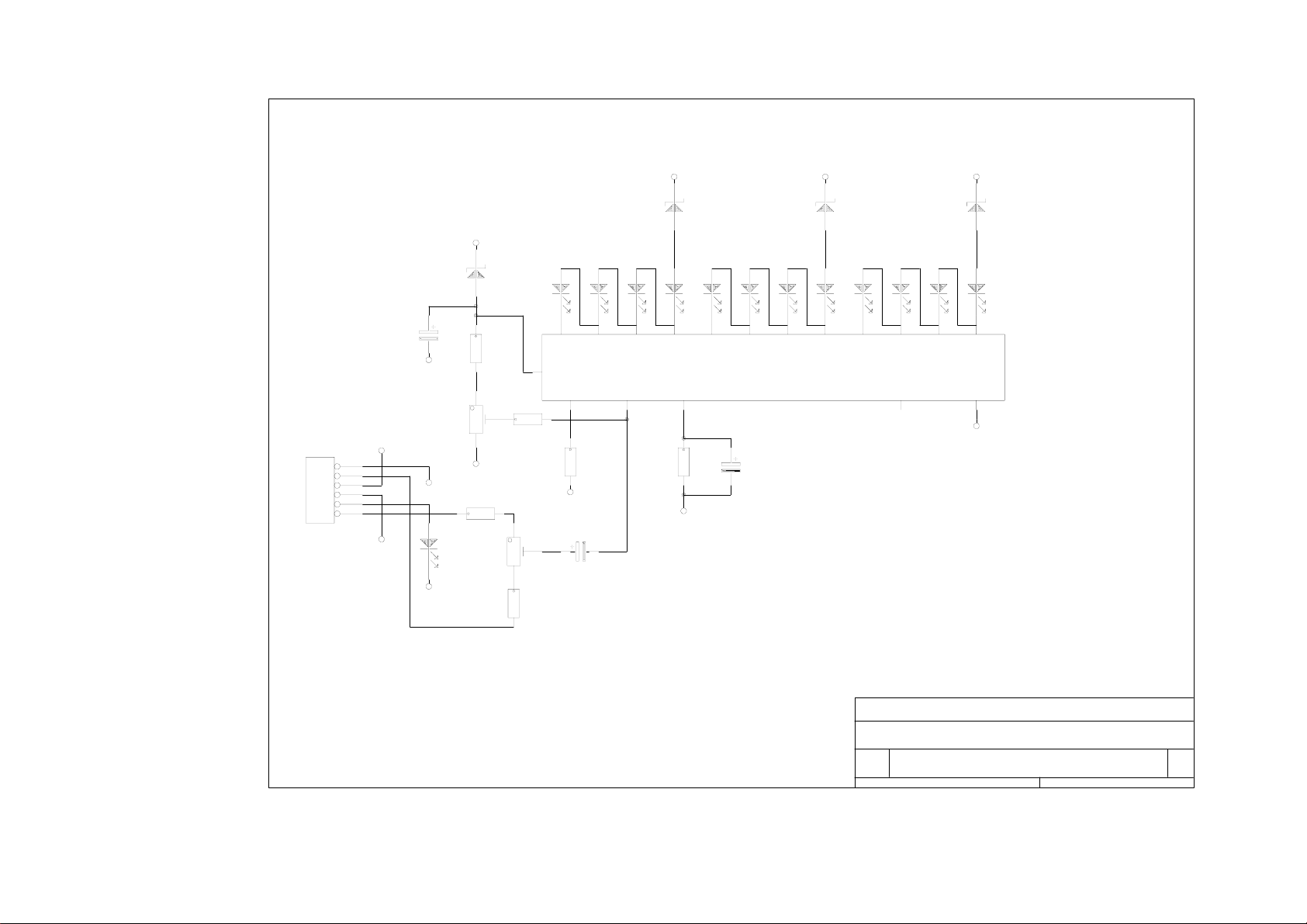
V+LEDSV+LEDSV+LEDS
CON1S
6WAY
MH12.5
V+LEDS
6
5
4
3
2
1
V-LEDS
CENTRE
PEAK
C1S
22U
25VLP
V+LEDS
V-LEDS
PR2S
500R
1/4V R4S
V-LEDS
V-S
RED
LED13S
V-S
R1S
22K
R3S
270K
-21dB
ADJ
D1S
18V
1
10K
+12
PR1S
5K
1/4V
R2S
2K2
LED12S
RED
V+
V-LEDS
D2S
18V
LED9S
RED
LED10S
LED11S
RED
RED
5
6
D
1
2
I
2
7
D
D
1
1
1
0
I
/
P
3
LED8S
GRN
1
8
0
D
D
9
8
T
/
C
4
LED7S
GRN
LED6S
GRN
1
1
1
2
D
D
7
6
CENTRE METER
R5S
47K
C2S
2U2
50VLP
R6S
10K C3S
V-LEDS
10U
16VLP
1
3
D
5
D3S
18V
LED5S
GRN
LED4S
GRN
D4S
18V
1
6
V-LEDS
1
7
D
1
0
V
9
LED1S
GRN
-21
IC1S
BA683A
GRN
LED2S
GRN
1
5
D
D
3
2
D
O
T
1
8
LED3S
1
4
D
4
METER SUB BOARD
DDA, HOUNSLOW, MIDDX, TW3 2EB, ENGLAND.
Title
CS3 METER BOARD (CENTRE METER)
Size Document Number REV
A CD1273-1 & PC1385-1 C
Date: January 23, 1996 Sheet 1 of 1

0V IN
AC IN
AC IN
CON1
3
2
1
3WAY
METWAY
100N
C23
33U
100V
R1
1R
TR1
ZTX553
R2
10K
220U
100V
1N4002
C2
220U
100V
1N4002
D3
C4
C3
100N
470U
0.2
D5
100V
D2
1N4002
C1
1N4002
D4
Voltage
Doubler
+18V-18V
C26
C21
KBU802
100N
0.2
BR2
C22
100N
0.2
C8
100N
0.2
C13
100N
C9
15000U
35V
C14
15000U
35V
120R
120R
R15
R8
0R1
2.5W/W
R7
C10
1000U
C15
1000U
40V
TR5
BC212
R9
680R
40V
C11
10N
C16
10N
0.2
R17
680R
TR10
BC182
R16
0R1
2.5W/W
C19
0.2
BR1
KBU802
C20
100N
0.2
8 Amp 100VBridge
R28
33U
7K5
63V0.2
TR7
TIP31A
VERT
TR16
BC182
D10
TR17
BC212
R32
7K5
C31
33U63V0.2
C5
33U
100V
R12
4K7
TR8
2N3055-REV
R10
10K
TR6
BC182
TR11
BC212
R18
10K
TR12
TIP32A
VERT
TR13
MJ2955-REV
R20
4K7
R3
10K
FITTED
R24
R25
R26
15K
10K
220R
TR4
TIP31C
VERT
TR3
ZTX453
R4
10K
C6
10N
0.2
ZTX453
NOT
R13
470R
D8
16V
PR2
5K
1/4V
R11
2K4
R30
10K
R31
R19
10K
2K4
PR3
5K
1/4V
R21
470R
TR2
D12
1N4148
D11
1N4148
D9
16V
C27
470N
0.2
C24
470N
0.2
R5
2K4
TR9
BC212
R34
680R
C32
470N
0.2
C33
470N
0.2
R35
680R
C30
470N
0.2
2K2
TR14
BC182
D6
16V
D7
22V
PR1
50K
1/4V
R6
D13
1N4148
C34
470N
0.2
R29
10K
C28
470N
0.2
C29
470N
0.2
R33
10K
R27
10K
TR15
ZTX553
C25
470N
0.2
NOT
FITTED
C12
220U
25V
C17
220U
25V
KLARK TEKNIK - DDA DIVISION
INWOOD BUSINESS PARK, HOUNSLOW, MIDDX, TW3 2
HOUNSLOW, TW3 2EB
Title
Size Document Number REV
B CD1271-1 & PC1386-1 C
Date: January 23, 1996 Sheet 1 of 1
+48V
C7
33U
63V0.2
+18V
-18V
CS3 PSU BOARD
C18
100N
CON2
8
7
6
5
4
3
2
1
8WAY
METWAY
EARTH
EARTH
EARTH
0V
+48V
+18V
0V
-18V
R23
100R
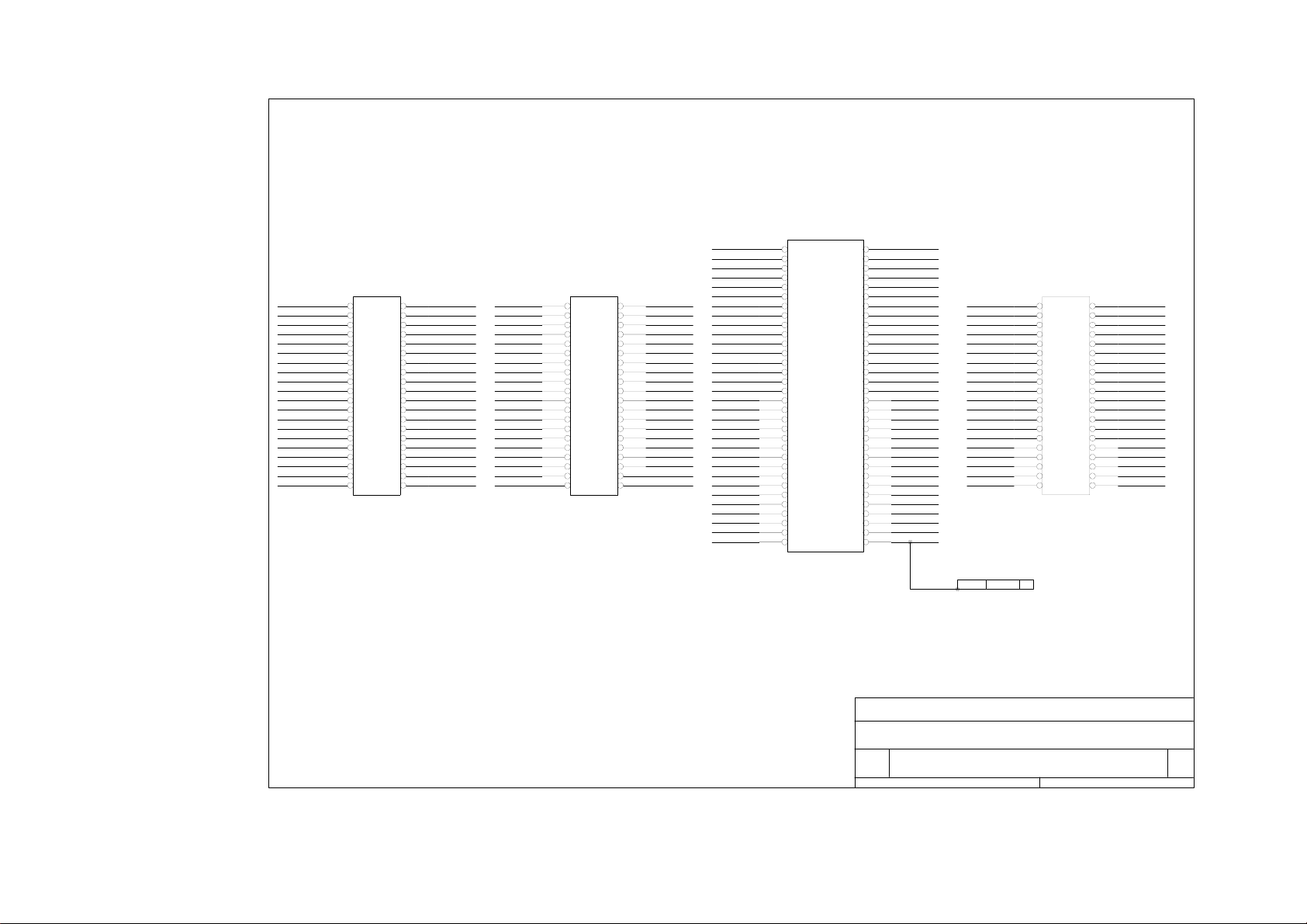
SEND8
SEND7
SEND6
SEND5
SEND4
SEND3
SEND2
SEND1
SENDR
SENDC
SENDL
AUXIP8
AUXIP7
AUXIP6
AUXIP5
AUXIP4
AUXIP3
AUXIP2
AUXIP1
CLEAN0V
Input Input
CON1
12
34
56
78
910
11 12
13 14
15 16
17 18
19 20
21 22
23 24
25 26
27 28
29 30
31 32
33 34
35 36
37 38
39 40
40WAY
IDCMD
MUTE1IP
MUTE2IP
MUTE3IP
MUTE4IP
CUESEND
CUEDC
SIPREC
BUSREF
+18V
+18V
+18V
0V
0V
0V
-18V
-18V
-18V
+48V
SEND8
SEND7
SEND6
SEND5
SEND4
SEND3
SEND2
SEND1
SENDR
SENDC
SENDL
AUXIP8
AUXIP7
AUXIP6
AUXIP5
AUXIP4
AUXIP3
AUXIP2
AUXIP1
CLEAN0V
CON2
12
34
56
78
910
11 12
13 14
15 16
17 18
19 20
21 22
23 24
25 26
27 28
29 30
31 32
33 34
35 36
37 38
39 40
40WAY
IDCMD
MUTE1IP
MUTE2IP
MUTE3IP
MUTE4IP
CUESEND
CUEDC
SIPREC
BUSREF
+18V
+18V
+18V
0V
0V
0V
-18V
-18V
-18V
+48V
SEND8
SEND7
SEND6
SEND5
SEND4
SEND3
SEND2
SEND1
SENDR
SENDC
SENDL
AUXIP8
AUXIP7
AUXIP6
AUXIP5
AUXIP4
AUXIP3
AUXIP2
AUXIP1
CUESEND
CUEDC
SIPREC
BUSREF
0V
0V
0V
0V
MUTE1IP
MUTE2IP
MUTE3IP
MUTE4IP
MWK
CON3
2B
64WAY-MALE
Mounted on track
side of pcb.
1A1B
2A
3A3B
4A4B
5A5B
6A6B
7A7B
8A8B
9A9B
10A10B
11A11B
12A12B
13A13B
14A14B
15A15B
16A16B
17A17B
18A18B
19A19B
20A20B
21A21B
22A22B
23A23B
24A24B
25A25B
26A26B
27A27B
28A28B
29A29B
30A30B
31A31B
32A32B
BUS8
BUS7
BUS6
BUS5
BUS4
BUS3
BUS2
BUS1
MIXR
MIXC
MIXL
AUX8
AUX7
AUX6
AUX5
AUX4
AUX3
AUX2
AUX1
IPCUE
IPCUEDC
BUSREF
MUTE1
MUTE2
MUTE3
MUTE4
SIP
0V
0V
0V
0V
MWK
BUS7
BUS6
BUS5
BUS4
BUS3
BUS2
BUS1
MIXR
MIXC
MIXL
AUX8
AUX7
AUX6
AUX5
AUX4
AUX3
AUX2
AUX1
CLEAN0V
2 PL1
1
1/4RPB
Output
CON4
12
34
56
78
910
11 12
13 14
15 16
17 18
19 20
21 22
23 24
25 26
27 28
29 30
31 32
33 34
35 36
37 38
39 40
40WAY
IDCMD
MWK CON
UNFITTED
MUTE1BUS8
MUTE2
MUTE3
MUTE4
IPCUE
IPCUEDC
BUSREF
+18V
+18V
+18V
-18V
-18V
-18V
+48V
SIP
0V
0V
0V
DDA, HOUNSLOW, MIDDX, TW3 2EB, ENGLAND.
Title
Size Document Number REV
A CD1306-1 A
Date: February 6, 1997 Sheet 1 of 1
CS8 BUS LINK

BUS8
BUS7
BUS6
BUS5
BUS4
BUS3
BUS2
BUS1
MIXR
MIXC
MIXL
AUX8
AUX7
AUX6
AUX5
AUX4
AUX3
AUX2
AUX1
IPCUE
IPCUEDC
SIP
BUS_REF BUS_REF
0V
0V
0V
0V
MUTE1
MUTE2
MUTE3
MUTE4
CON1
2B
64WAY
DFINV
1A1B
2A
3A3B
4A4B
5A5B
6A6B
7A7B
8A8B
9A9B
10A10B
11A11B
12A12B
13A13B
14A14B
15A15B
16A16B
17A17B
18A18B
19A19B
20A20B
21A21B
22A22B
23A23B
24A24B
25A25B
26A26B
27A27B
28A28B
29A29B
30A30B
31A31B
32A32B
BUS8
BUS7
BUS6
BUS5
BUS4
BUS3
BUS2
BUS1
MIXR
MIXC
MIXL
AUX8
AUX7
AUX6
AUX5
AUX4
AUX3
AUX2
AUX1
IPCUE
IPCUEDC
MUTE1
MUTE2
MUTE3
MUTE4
SIP
0V
0V
0V
0V
MWKMWK
DDA, HOUNSLOW, MIDDX, TW3 2EB, ENGLAND.
Title
CS8 BUS LINK BLANKING PLUG
Size Document Number REV
A CD1308-1 A
Date: February 12, 1997 Sheet 1 of 1

V+
D1
1N4148
0.4"
D2
1N4148
0.4"
R17
22K
V-
This drawing is split across the following two pages to aid readability .
R3
270R
-21
5
R4
75R
R6
120R
R7
180R
R8
270R
R9
360R
R10
510R
R11
820R
R12
1K
R13
1K5
R14
2K
R15
3K
R16
24K
V+
+
4
-
7
+
6
-18
-
9
+
8
-
11
+
10
-
-15
LM2901
-12
-9
5
+
4
-
7
+
6
-6
-
9
+
8
-
11
+
10
-
-3
LM2901
0
+3
5
+
4
-
7
+
6
+6
-
9
+
8
-
11
+
10
-
+9
LM2901
+12
V+ V+
R18
120R
TR1
BC212
AI
V+
LED1
GRN
3
2
O
+
V
1
O
14
O
13
O
V
12IC1
V-
V+
3
2
O
+
V
1
O
14
O
13
O
V
12IC2
V-
V+
3
2
O
+
V
1
O
14
O
13
O
V
12IC3
V-
-21
LED2
-18
GRN
-15
LED3
GRN
-12
LED4
GRN
LED5
GRN
-9
LED6
-6
GRN
-3
LED7
GRN
0
LED8
YEL
LED9
YEL
+3
LED10
+6
YEL
+9
LED11
YEL
+12
LED12
RED
V- V-
R19
120R
TR2
BC212
AI
V+
LED13
GRN
3
5
+
O
+
4
V
-
7
+
O
6
-
9
+
O
8
-
11
+
O
-
10
-
V
12IC4
LM2901
V-
V+
3
5
+
O
+
4
V
-
7
+
O
6
-
9
+
O
8
-
11
+
O
-
10
-
V
12IC5
LM2901
V-
V+
3
5
+
O
+
4
V
-
7
+
O
6
-
9
+
O
8
-
11
+
O
-
10
-
V
12IC6
LM2901
V-
-21
2
1
LED14
GRN
14
13
LED15
GRN
LED16
GRN
LED17
GRN
2
1
LED18
GRN
14
13
LED19
GRN
LED20
YEL
LED21
YEL
2
1
LED22
YEL
14
13
LED23
YEL
LED24
RED
5
+
4
-
7
+
6
-18
-
9
+
8
-
11
+
10
-
-15
LM2901
-12
-9
5
+
4
-
7
+
6
-6
-
9
+
8
-
11
+
10
-
-3
LM2901
0
+3
5
+
4
-
7
+
6
+6
-
9
+
8
-
11
+
10
-
+9
LM2901
+12
V+
R20
120R
TR3
BC212
AI
V+
LED25
GRN
3
2
O
+
V
1
O
14
O
13
O
V
12IC7
V-
V+
3
2
O
+
V
1
O
14
O
13
O
V
12IC8
V-
V+
3
2
O
+
V
1
O
14
O
13
O
V
12IC9
V-
-21
5
4
LED26
GRN
LED27
GRN
LED28
GRN
LED29
GRN
LED30
GRN
LED31
GRN
LED32
YEL
LED33
YEL
LED34
YEL
LED35
YEL
LED36
RED
V-
7
6
-18
9
8
11
10
-15
LM2901
-12
-9
5
4
7
6
-6
9
8
11
10
-3
LM2901
0
+3
5
4
7
6
+6
9
8
11
10
+9
LM2901
+12
V+
R21
120R
TR4
BC212
AI
V+
LED37
GRN
3
2
+
O
+
V
1
+
O
14
+
O
13
+
O
-
-
V
12IC10
V-
V+
3
2
+
O
+
V
1
+
O
14
+
O
13
+
O
-
-
V
12IC11
V-
V+
3
2
+
O
+
V
1
+
O
14
+
O
13
+
O
-
-
V
12IC12
V-
-21
5
4
LED38
GRN
LED39
GRN
LED40
GRN
LED41
GRN
LED42
GRN
LED43
GRN
LED44
YEL
LED45
YEL
LED46
YEL
LED47
YEL
LED48
RED
V-
7
6
-18
9
8
11
10
-15
LM2901
-12
-9
5
4
7
6
-6
9
8
11
10
-3
LM2901
0
+3
5
4
7
6
+6
9
8
11
10
+9
LM2901
+12
V+
R22
120R
TR5
BC212
AI
V+
LED49
GRN
3
2
+
O
+
V
1
+
O
14
+
O
13
+
O
-
-
V
12IC13
V-
V+
3
2
+
O
+
V
1
+
O
14
+
O
13
+
O
-
-
V
12IC14
V-
V+
3
2
+
O
+
V
1
+
O
14
+
O
13
+
O
-
-
V
12IC15
V-
-21 -21
5
+
4
-
7
LED50
GRN
LED51
GRN
LED52
GRN
LED53
GRN
LED54
GRN
LED55
GRN
LED56
YEL
LED57
YEL
LED58
YEL
LED59
YEL
LED60
RED
V-
+
6
-18 -18
-
9
+
8
-
11
+
10
-
-15 -15
LM2901
-12 -12
-9 -9
5
+
4
-
7
+
6
-6 -6
-
9
+
8
-
11
+
10
-
-3 -3
LM2901
0
+3 +3
5
+
4
-
7
+
6
+6
-
9
+
8
-
11
+
10
-
+9
LM2901
+12
V+
R23
120R
TR6
BC212
AI
V+
LED61
GRN
3
2
O
+
V
1
O
LED62
GRN
14
O
13
O
V
LED63
121C16
GRN
V-
LED64
GRN
V+
LED65
GRN
3
2
O
+
V
1
O
LED66
GRN
14
O
13
O
V
LED67
12IC17
GRN
V-
LED68
YEL
V+
LED69
YEL
3
2
O
+
V
1
O
LED70
YEL
14
O
13
O
V
LED71
12IC18
YEL
V-
LED72
RED
V-
5
+
4
-
7
+
6
-
9
+
8
-
11
+
10
-
LM2901
5
+
4
-
7
+
6
-
9
+
8
-
11
+
10
-
LM2901
00
5
+
4
-
7
+
6
+6 +6
-
9
+
8
-
11
+
10
-
+9 +9
LM2901
+12 +12
V+
R24
120R
TR7
BC212
AI
V+
LED73
GRN
3
2
O
+
V
1
O
14
O
13
O
V
12IC19
V-
V+
3
2
O
+
V
1
O
14
O
13
O
V
12IC20
V-
V+
3
2
O
+
V
1
O
14
O
13
O
V
12IC21
V-
-21
5
4
LED74
GRN
LED75
GRN
LED76
GRN
LED77
GRN
LED78
GRN
LED79
GRN
LED80
YEL
LED81
YEL
LED82
YEL
LED83
YEL
LED84
RED
V-
7
6
-18
9
8
11
10
-15
LM2901
-12
-9
5
4
7
6
-6
9
8
11
10
-3
LM2901
+3
5
4
7
6
9
8
11
10
LM2901
V+
R25
120R
TR8
BC212
AI
V+
LED85
GRN
3
2
+
O
+
V
1
+
O
-
+
-
+
-
+
-
+
-
+
-
+
-
+
-
+
-
+
-
+
-
LED86
GRN
14
O
13
O
V
LED87
12IC22
GRN
V-
LED88
GRN
V+
LED89
GRN
3
2
O
+
V
1
O
LED90
GRN
14
O
13
O
V
LED91
12IC23
GRN
V-
LED92
YEL
V+
LED93
YEL
3
2
O
+
V
1
O
LED94
YEL
14
O
13
O
V
LED95
12IC24
YEL
V-
LED96
RED
V-
METER-5
V+
IC25A
4
TL074
3
1
CON1
1
2
3
4
METER-5
5
METER-6
6
METER-7
7
METER-8
8
9
10
11
12
13
14
14WAY
IDCMD
R2
R1
10R
10R
C1
C2
220U
220U
25V
25V
V+
C4
C5
C6
220N
220N
C3
220N
R34
4M7
V-
220N
R35
R36
4M7
4M7
2
1
1
IC25B
V-
TL074
5
7
6
IC25C
TL074
10
8
9
IC25D
R37
4M7
TL074
12
14
13
C7
220N
220N
R38
4M7
R39
4M7
METER-6
METER-7
C8
C9
220N
METER-8
R41
4M7
R40
C10
4M7
220N
1
2
1
1
IC26B
V-
TL074
5
7
6
IC26C
TL074
10
8
9
IC26D
TL074
12
14
13
LAST R R41
LAST C
LAST CON
LAST D
LAST LED
LAST IC
DDA, HOUNSLOW, MIDDX, TW3 2EB, ENGLAND.
Title
C10
CON1
D2
LED96
IC26
CS8 INPUT METER PCB
Size Document Number REV
D CD1307-1 A
Date: March 6, 1997 Sheet 1 of 1
V+
IC26A
4
TL074
3
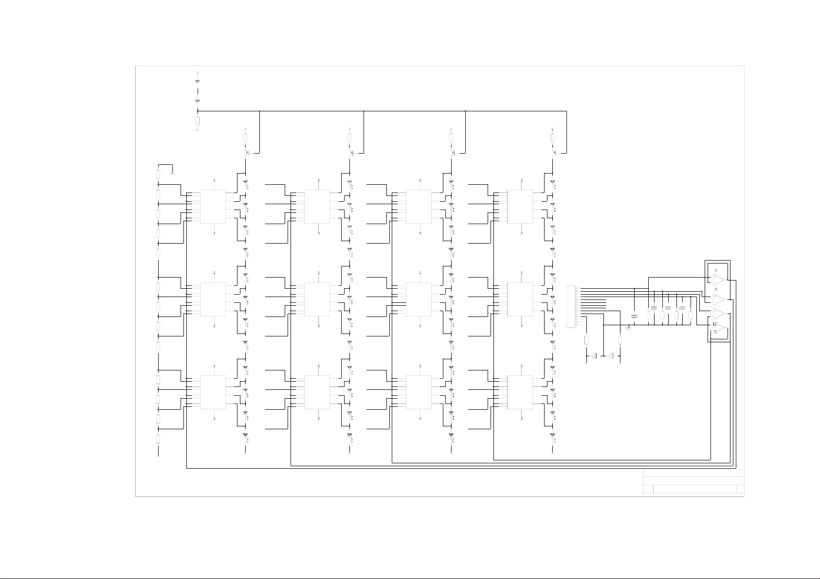
V+
D1
1N4148
0.4"
D2
1N4148
0.4"
R17
22K
V-
R3
270R
-21
R4
75R
-18
R6
120R
-15
R7
180R
-12
R8
270R
-9
R9
360R
-6
R10
510R
-3
R11
820R
0
R12
1K
+3
R13
1K5
+6
R14
2K
+9
R15
3K
+12
R16
24K
V+
5
+
+
4
V
-
7
+
6
-
9
+
8
-
11
+
-
10
-
V
LM2901
V-
V+
5
+
+
4
V
-
7
+
6
-
9
+
8
-
11
+
-
10
-
V
LM2901
V-
V+
5
+
+
4
V
-
7
+
6
-
9
+
8
-
11
+
-
10
-
V
LM2901
V-
V+
V+
R18
120R
TR1
BC212
AI
LED1
GRN
3
2
O
1
O
14
O
13
O
12IC1
3
2
O
1
O
14
O
13
O
12IC2
3
2
O
1
O
14
O
13
O
12IC3
-21
LED2
-18
GRN
-15
LED3
GRN
-12
LED4
GRN
LED5
GRN
-9
LED6
-6
GRN
-3
LED7
GRN
0
LED8
YEL
LED9
YEL
+3
LED10
+6
YEL
+9
LED11
YEL
+12
LED12
RED
V+
5
+
+
4
V
-
7
+
6
-
9
+
8
-
11
+
-
10
-
V
LM2901
V-
V+
5
+
+
4
V
-
7
+
6
-
9
+
8
-
11
+
-
10
-
V
LM2901
V-
V+
5
+
+
4
V
-
7
+
6
-
9
+
8
-
11
+
-
10
-
V
LM2901
V-
V+
R19
120R
TR2
BC212
AI
LED13
GRN
3
2
O
1
O
14
O
13
O
12IC4
3
2
O
1
O
14
O
13
O
12IC5
3
2
O
1
O
14
O
13
O
12IC6
-21
LED14
-18
GRN
-15
LED15
GRN
-12
LED16
GRN
LED17
GRN
-9
LED18
-6
GRN
-3
LED19
GRN
0
LED20
YEL
LED21
YEL
+3
LED22
+6
YEL
+9
LED23
YEL
+12
LED24
RED
V+
5
+
+
4
V
-
7
+
6
-
9
+
8
-
11
+
-
10
-
V
LM2901
V-
V+
5
+
+
4
V
-
7
+
6
-
9
+
8
-
11
+
-
10
-
V
LM2901
V-
V+
5
+
+
4
V
-
7
+
6
-
9
+
8
-
11
+
-
10
-
V
LM2901
V-
V+
R20
120R
TR3
BC212
AI
LED25
GRN
3
2
O
1
O
14
O
13
O
12IC7
3
2
O
1
O
14
O
13
O
12IC8
3
2
O
1
O
14
O
13
O
12IC9
-21
LED26
-18
GRN
-15
LED27
GRN
-12
LED28
GRN
LED29
GRN
-9
LED30
-6
GRN
-3
LED31
GRN
0
LED32
YEL
LED33
YEL
+3
LED34
+6
YEL
+9
LED35
YEL
+12
LED36
RED
V- V- V- V-
5
+
4
-
7
+
6
-
9
+
8
-
11
+
10
-
LM2901
5
+
4
-
7
+
6
-
9
+
8
-
11
+
10
-
LM2901
5
+
4
-
7
+
6
-
9
+
8
-
11
+
10
-
LM2901
CURRENT REF
V+
R21
120R
TR4
BC212
AI
V+
3
+
V
V
12IC10
LED37
GRN
2
O
1
O
LED38
GRN
14
O
13
O
LED39
GRN
V-
LED40
GRN
V+
3
+
V
V
12IC11
V-
V+
3
+
V
V
12IC12
LED41
GRN
2
O
1
O
14
O
13
O
2
O
1
O
14
O
13
O
CON1
1
LED42
2
GRN
3
4
METER-5
5
METER-6
6
METER-7
7
METER-8
8
9
LED43
10
GRN
11
12
13
14
14WAY
IDCMD
R1
LED44
YEL
10R
C1
220U
25V
V+
LED45
YEL
LED46
YEL
LED47
YEL
220N
R2
10R
C2
220U
25V
V-
C4
C5
220N
C3
R34
4M7
C6
220N
220N
R35
R36
R37
4M7
4M7
4M7
V+
4
3
1
2
IC25A
1
TL074
1
IC25B
V-
TL074
5
7
6
IC25C
10
TL074
8
9
IC25D
12
TL074
14
13
V-
LED48
RED
Klark Teknik - DDA Division
Title
Size Document Number REV
Date: May 1, 1997 Sheet 1 of 2
CS8 - INPUT METER
C CD1307-1 A

CURRENT REF
V+
R22
120R
TR5
BC212
AI
-21
-18
-15
-12
-9
V+
IC26A
4
TL074
METER-5
METER-6
METER-7
C8
C9
C7
220N
R38
4M7
220N
220N
R39
4M7
METER-8
R41
4M7
R40
C10
4M7
220N
3
1
2
1
1
IC26B
V-
TL074
5
7
6
IC26C
10
TL074
8
9
IC26D
TL074
12
14
13
-6
-3
0
+3
+6
+9
+12
V+
3
5
+
O
+
4
V
-
7
+
LM2901
O
+
O
+
O
-
-
V
12IC13
V-
6
9
8
11
10
V+
3
5
4
7
6
9
8
11
10
LM2901
O
+
+
V
+
O
+
O
+
O
-
-
V
12IC14
V-
V+
3
5
+
O
+
4
V
-
7
+
LM2901
O
O
+
-
+
O
-
-
V
12IC15
V-
6
9
8
11
10
LED49
GRN
-21
2
1
LED50
-18
GRN
14
13
-15
LED51
GRN
-12
LED52
GRN
LED53
GRN
-9
2
1
LED54
-6
GRN
14
13
-3
LED55
GRN
0
LED56
YEL
LED57
YEL
+3
2
1
LED58
+6
YEL
14
13
+9
LED59
YEL
+12
LED60
RED
V+
5
+
+
4
V
-
7
+
6
-
9
+
8
-
11
+
-
10
-
V
LM2901
V-
V+
5
+
+
4
V
-
7
+
6
-
9
+
8
-
11
+
-
10
-
V
LM2901
V-
V+
5
+
+
4
V
-
7
+
6
-
9
+
8
-
11
+
-
10
-
V
LM2901
V-
V+
R23
120R
TR6
BC212
AI
LED61
GRN
3
2
O
1
O
14
O
13
O
121C16
3
2
O
1
O
14
O
13
O
12IC17
3
2
O
1
O
14
O
13
O
12IC18
-21
LED62
-18
GRN
-15
LED63
GRN
-12
LED64
GRN
LED65
GRN
-9
LED66
-6
GRN
-3
LED67
GRN
0
LED68
YEL
LED69
YEL
+3
LED70
+6
YEL
+9
LED71
YEL
+12
LED72
RED
V+
5
+
+
4
V
-
7
+
6
-
9
+
8
-
11
+
-
10
-
V
LM2901
V-
V+
5
+
+
4
V
-
7
+
6
-
9
+
8
-
11
+
-
10
-
V
LM2901
V-
V+
5
+
+
4
V
-
7
+
6
-
9
+
8
-
11
+
-
10
-
V
LM2901
V-
V+
R24
120R
TR7
BC212
AI
LED73
GRN
3
2
O
1
O
14
O
13
O
12IC19
3
2
O
1
O
14
O
13
O
12IC20
3
2
O
1
O
14
O
13
O
12IC21
-21
LED74
-18
GRN
-15
LED75
GRN
-12
LED76
GRN
LED77
GRN
-9
LED78
-6
GRN
-3
LED79
GRN
0
LED80
YEL
LED81
YEL
+3
LED82
+6
YEL
+9
LED83
YEL
+12
LED84
RED
V+
5
+
+
4
V
-
7
+
6
-
9
+
8
-
11
+
-
10
-
V
LM2901
V-
V+
5
+
+
4
V
-
7
+
6
-
9
+
8
-
11
+
-
10
-
V
LM2901
V-
V+
5
+
+
4
V
-
7
+
6
-
9
+
8
-
11
+
-
10
-
V
LM2901
V-
V+
R25
120R
TR8
BC212
AI
LED85
3
O
O
O
O
12IC22
3
O
O
O
O
12IC23
3
O
O
O
O
12IC24
GRN
2
1
LED86
GRN
14
13
LED87
GRN
LED88
GRN
LED89
GRN
2
1
LED90
GRN
14
13
LED91
GRN
LED92
YEL
LED93
YEL
2
1
LED94
YEL
14
13
LED95
YEL
LED96
RED
V-
V-
V-
Title
Size Document Number REV
C CD1307-1 A
Date: May 1, 1997 Sheet 2 of 2
V-
Klark Teknik - DDA Division
CS8 - INPUT METER

V+
D1
D2
1N4148
1N4148
0.4"R17
0.4"
BASEREF
22K
V-
R3
270R
-21
R4
75R
-18
R6
120R
-15
R7
This drawing is split across the following three pages to aid readability .
180R
-12
R8
270R
-9
R9
360R
-6
R10
510R
-3
R11
820R
0
R12
1K
+3
R13
1K5
+6
R14
2K
+9
R15
3K
+12
R16
30K
V+
-21
-18
-15
-12
-9
-6
-3
0
+3
+6
+9
+12
V+
3
5
2
+
O
+
4
V
-
7
1
+
O
6
-
9
14
+
O
8
-
11
13
+
O
-
10
-
V
12IC1
LM2901
V-
V+
3
5
2
+
O
+
4
V
-
7
1
+
O
6
-
9
14
+
O
8
-
11
13
+
O
-
10
-
V
12IC2
LM2901
V-
V+
3
5
2
+
O
+
4
V
-
7
1
+
O
6
-
9
14
+
O
8
-
11
13
+
O
-
10
-
V
12IC3
LM2901
V-
METER1
BASEREF
V+
3
5
2
+
O
+
4
V
-
7
1
+
O
6
-
9
14
+
O
8
-
11
13
+
O
-
10
-
V
12IC25
LM2901
V-
V+
3
5
2
+
O
+
4
V
-
7
1
+
O
6
-
9
14
+
O
8
-
11
13
+
O
-
10
-
V
12IC26
LM2901
V-
V+
3
5
2
+
O
+
4
V
-
7
1
+
O
6
-
9
14
+
O
8
-
11
13
+
O
-
10
-
V
12IC27
LM2901
V-
RECTL
V-
V+
R18
TR1
120R
BC212
AI
LED1
GRN
-21
LED2
-18
GRN
-15
LED3
GRN
-12
LED4
GRN
LED5
GRN
-9
LED6
-6
GRN
-3
LED7
GRN
LED8
YEL
LED9
YEL
+3
LED10
+6
YEL
+9
LED11
YEL
+12
LED12
RED
V-
V+
R26
TR9
120R
BC212
AI
LED97
GRN
-21
LED98
-18
GRN
-15
LED99
GRN
-12
LED100
GRN
LED101
GRN
-9
LED102
-6
GRN
-3
LED103
GRN
0
LED104
YEL
LED105
YEL
+3
LED106
+6
YEL
+9
LED107
YEL
+12
LED108
RED
V+
3
5
+
O
+
4
V
-
7
+
O
6
-
9
+
O
8
-
11
+
O
-
10
-
V
12IC4
LM2901
V-
V+
3
5
+
O
+
4
V
-
7
+
O
6
-
9
+
O
8
-
11
+
O
-
10
-
V
12IC5
LM2901
V-
0
V+
3
5
+
O
+
4
V
-
7
+
O
6
-
9
+
O
8
-
11
+
O
-
10
-
V
12IC6
LM2901
V-
METER2
V+
3
5
2
+
O
+
4
V
-
7
1
+
O
6
-
9
14
+
O
8
-
11
13
+
O
-
10
-
V
12IC28
LM2901
V-
V+
3
5
2
+
O
+
4
V
-
7
1
+
O
6
-
9
14
+
O
8
-
11
13
+
O
-
10
-
V
12IC29
LM2901
V-
V+
3
5
2
+
O
+
4
V
-
7
1
+
O
6
-
9
14
+
O
8
-
11
13
+
O
-
10
-
V
12IC30
LM2901
V-
RECTC
V-
V+
R19
TR2
120R
BC212
AI
LED13
GRN
-21
2
1
LED14
-18
GRN
14
13
-15
LED15
GRN
-12
LED16
GRN
LED17
GRN
-9
2
1
LED18
-6
GRN
14
13
-3
LED19
GRN
0
LED20
YEL
LED21
YEL
2
1
14
13
+3
LED22
+6
YEL
+9
LED23
YEL
+12
LED24
RED
V-
V+
R27
TR10
120R
BC212
AI
LED109
GRN
-21
LED110
-18
GRN
-15
LED111
GRN
-12
LED112
GRN
LED113
GRN
-9
LED114
-6
GRN
-3
LED115
GRN
0
LED116
YEL
LED117
YEL
+3
LED118
+6
YEL
+9
LED119
YEL
+12
LED120
RED
V+
3
5
2
+
O
+
4
V
-
7
1
+
O
6
-
9
14
+
O
8
-
11
13
+
O
-
10
-
V
12IC7
LM2901
V-
V+
3
5
2
+
O
+
4
V
-
7
1
+
O
6
-
9
14
+
O
8
-
11
13
+
O
-
10
-
V
12IC8
LM2901
V-
V+
3
5
2
+
O
+
4
V
-
7
1
+
O
6
-
9
14
+
O
8
-
11
13
+
O
-
10
-
V
12IC9
LM2901
V-
METER3
V+
3
5
2
+
O
+
4
V
-
7
1
+
O
6
-
9
14
+
O
8
-
11
13
+
O
-
10
-
V
12IC31
LM2901
V-
V+
3
5
2
+
O
+
4
V
-
7
1
+
O
6
-
9
14
+
O
8
-
11
13
+
O
-
10
-
V
12IC32
LM2901
V-
V+
3
5
2
+
O
+
4
V
-
7
1
+
O
6
-
9
14
+
O
8
-
11
13
+
O
-
10
-
V
12IC33
LM2901
V-
RECTR
V-
V+
R20
TR3
120R
BC212
AI
LED25
GRN
-21
LED26
-18
GRN
-15
LED27
GRN
-12
LED28
GRN
LED29
GRN
-9
LED30
-6
GRN
-3
LED31
GRN
0
LED32
YEL
LED33
YEL
+3
LED34
+6
YEL
+9
LED35
YEL
+12
LED36
RED
V-
V+
R28
TR11
120R
BC212
AI
LED121
GRN
LED122
GRN
LED123
GRN
LED124
GRN
LED125
GRN
LED126
GRN
LED127
GRN
LED128
YEL
LED129
YEL
LED130
YEL
LED131
YEL
LED132
RED
V+
3
5
2
+
O
+
4
V
-
7
1
+
O
6
-
9
14
+
O
8
-
11
13
+
O
-
10
-
V
12IC10
LM2901
V-
V+
3
5
2
+
O
+
4
V
-
7
1
+
O
6
-
9
14
+
O
8
-
11
13
+
O
-
10
-
V
12IC11
LM2901
V-
V+
3
5
2
+
O
+
4
V
-
7
1
+
O
6
-
9
14
+
O
8
-
11
13
+
O
-
10
-
V
12IC12
LM2901
V-
METER4
CON2
METER1
1
METER2
2
METER3
3
METER4
4
METER5
5
METER6
6
METER7
7
METER8
8
RECTL
9
RECTC
10
10WAY
FHV
V+
R21
TR4
120R
BC212
AI
LED37
GRN
-21
LED38
-18
GRN
-15
LED39
GRN
-12
LED40
GRN
LED41
GRN
-9
LED42
-6
GRN
-3
LED43
GRN
0
LED44
YEL
LED45
YEL
+3
LED46
+6
YEL
+9
LED47
YEL
+12
LED48
RED
V-
V+
CON3
1
2
2WAY
V+
3
5
2
+
O
+
4
V
-
7
1
+
O
6
-
9
14
+
O
8
-
11
13
+
O
-
10
-
V
12IC13
LM2901
V-
V+
3
5
2
+
O
+
4
V
-
7
1
+
O
6
-
9
14
+
O
8
-
11
13
+
O
-
10
-
V
12IC14
LM2901
V-
V+
3
5
2
+
O
+
4
V
-
7
1
+
O
6
-
9
14
+
O
8
-
11
13
+
O
-
10
-
V
12IC15
LM2901
V-
METER5
PART OF SUB PCB
V+S
GROUP
R37
CON3S
1
2
10K
2WAY
WIR
ML
MATRIX
R38
10K
V+
R22
TR5
120R
BC212
AI
LED49
GRN
-21 -21
LED50
-18 -18
GRN
-15 -15
LED51
GRN
-12 -12
LED52
GRN
LED53
GRN
-9 -9
LED54
-6 -6
GRN
-3 -3
LED55
GRN
0
LED56
YEL
LED57
YEL
+3 +3
LED58
+6
YEL
+9
LED59
YEL
+12
LED60
RED
V-
C1
47N
CON4S
SW1
TP2301
SW3
TP2301
AUX
SW2
TP2301
CON4
1
1
2
2
2WAY
2WAY
ML
WIR
R30
100K
CON5S
CON5
1
1
2
2
2WAY
2WAY
ML
WIR
R33
100K
5
+
4
-
7
+
6
-
9
+
8
-
11
+
10
-
LM2901
5
+
4
-
7
+
6
-
9
+
8
-
11
+
10
-
LM2901
5
+
4
-
7
+
6
-
9
+
8
-
11
+
10
-
LM2901
METER6
VSS VSS
V+
3
+
V
V
12IC16
V-
V+
3
+
V
V
12IC17
V-
V+
3
+
V
V
12IC18
V-
R29
1K
C2
47N
R31
1K
C3
47N
VSSVSS
R23
V+ V+
TR6
120R
BC212
AI
LED61
GRN
2
O
1
O
LED62
GRN
14
O
13
O
LED63
GRN
LED64
GRN
LED65
GRN
2
O
1
O
LED66
GRN
14
O
13
O
LED67
GRN
00
LED68
YEL
LED69
YEL
2
O
1
O
LED70
+6 +6
YEL
14
O
13
O
+9 +9
LED71
YEL
+12 +12
LED72
RED
V-
V+
V-
V+
3
5
+
+
4
V
-
7
+
6
-
9
+
8
-
11
+
-
10
-
V
12IC19
LM2901
V-
V+
3
5
+
+
4
V
-
7
+
6
-
9
+
8
-
11
+
-
10
-
V
12IC20
LM2901
V-
V+
3
5
+
+
4
V
-
7
+
6
-
9
+
8
-
11
+
-
10
-
V
12IC21
LM2901
V-
METER7
GRPSW
AUXSW
MATSW
RECTR
GRPLED
AUXLED
MATLED
D3
6V8
0.4"
VSS
R39
360R
CON6
1
2
2WAY
ML
CON7
1
2
2WAY
ML
V-
O
O
O
O
O
O
O
O
O
O
O
O
CON1
1
2
3
4
5
6
7
8
9
10
10WAY
FHV
CON6S
CON7S
2WAY
WIR
2
1
14
13
2
1
14
13
2
1
14
13
1
2
2WAY
WIR
1
2
V-
V+S
2
4
6
8
10
12
14
16
R34
2K2
V+S
2
4
6
8
10
12
14
16
2
4
6
8
10
12
14
16
LAST R
LAST C
LAST CON
LAST D
LAST LED
LAST IC
LAST TR TR11
LAST SW SW3
R24
TR7
120R
BC212
AI
LED73
GRN
-21
5
4
LED74
GRN
LED75
GRN
LED76
GRN
LED77
GRN
LED78
GRN
LED79
GRN
LED80
YEL
LED81
YEL
LED82
YEL
LED83
YEL
LED84
RED
LED135
LEDBLK-RED
LED134
LEDBLK-RED
R35
2K2
LED133
LEDBLK-RED
R36
2K2
7
6
-18
9
8
11
10
-15
LM2901
-12
-9
5
4
7
6
-6
9
8
11
10
-3
LM2901
+3
5
4
7
6
9
8
11
10
LM2901
METER8
PART OF SUB PCB
1
3
5
7
MATRIX LED
9
11
13
15
1
3
5
7
AUX LED
9
11
13
15
1
3
5
7
GROUP LED
9
11
13
15
R51
DDA, HOUNSLOW, MIDDX, TW3 2EB, ENGLAND.
C3
CON7
Title
D5
LED135
Size Document Number REV
IC33
D CD1311-1 A
Date: March 21, 1997 Sheet 1 of 1
V+
3
+
O
+
V
+
O
+
O
+
O
-
-
V
12IC22
V-
V+
3
+
O
+
V
+
O
+
O
+
O
-
-
V
12IC23
V-
V+
3
+
O
+
V
+
O
+
O
+
O
-
-
V
12IC24
V-
CS8 LED OUTPUT METER PCB
2
1
14
13
2
1
14
13
2
1
14
13
V+
R25
TR8
120R
BC212
AI
LED85
GRN
LED86
GRN
LED87
GRN
LED88
GRN
LED89
GRN
LED90
GRN
LED91
GRN
LED92
YEL
LED93
YEL
LED94
YEL
LED95
YEL
LED96
RED
V-

CURRENT REF
-21
-18
-15
-12
-9
-6
-3
0
+3
+6
+9
+12
V+
3
5
4
7
6
9
8
11
10
LM2901
5
4
7
6
9
8
11
10
LM2901
5
4
7
6
9
8
11
10
LM2901
RECTL
2
+
O
+
V
1
+
O
14
+
O
13
+
O
-
-
V
12IC25
V-
V+
3
2
+
O
+
V
1
+
O
14
+
O
13
+
O
-
-
V
12IC26
V-
V+
3
2
+
O
+
V
1
+
O
14
O
+
13
+
O
-
-
V
12IC27
V-
V+
R26
TR9
120R
BC212
AI
LED97
GRN
-21
LED98
-18
GRN
-15
LED99
GRN
-12
LED100
GRN
LED101
GRN
-9
LED102
-6
GRN
-3
LED103
GRN
0
LED104
YEL
LED105
YEL
+3
LED106
+6
YEL
+9
LED107
YEL
+12
LED108
RED
V-
5
4
7
6
9
8
11
10
5
4
7
6
9
8
11
10
5
4
7
6
9
8
11
10
RECTC
LM2901
LM2901
LM2901
V+
3
2
+
O
+
V
1
+
O
14
+
O
13
+
O
-
-
V
12IC28
V-
V+
3
2
+
O
+
V
1
+
O
14
+
O
13
+
O
-
-
V
12IC29
V-
V+
3
2
+
O
+
V
1
+
O
14
O
+
13
+
O
-
-
V
12IC30
V-
V+
R27
TR10
120R
BC212
AI
LED109
GRN
-21
LED110
-18
GRN
-15
LED111
GRN
-12
LED112
GRN
LED113
GRN
-9
LED114
-6
GRN
-3
LED115
GRN
0
LED116
YEL
LED117
YEL
+3
LED118
+6
YEL
+9
LED119
YEL
+12
LED120
RED
V-
5
4
7
6
9
8
11
10
5
4
7
6
9
8
11
10
5
4
7
6
9
8
11
10
RECTR
LM2901
LM2901
LM2901
V+
3
2
+
O
+
V
1
+
O
14
+
O
13
+
O
-
-
V
12IC31
V-
V+
3
2
+
O
+
V
1
+
O
14
+
O
13
+
O
-
-
V
12IC32
V-
V+
3
2
+
O
+
V
1
+
O
14
O
+
13
+
O
-
-
V
12IC33
V-
V+R28
TR11
120R
V+
BC212
AI
LED121
GRN
LED122
GRN
LED123
GRN
LED124
GRN
LED125
GRN
LED126
GRN
LED127
GRN
LED128
YEL
LED129
YEL
LED130
YEL
LED131
YEL
LED132
RED
V-
CON6S
2WAY
WIR
CON7S
2WAY
WIR
CON3
1
2
2WAY
ML
R34
2K2
1
2
1
2
CON3S
2WAY
WIR
V+S
V+S
1
2
2
4
6
8
10
12
14
16
2
4
6
8
10
12
14
16
2
4
6
8
10
12
14
16
V+S
LED135
LEDBLK-RED
LED134
LEDBLK-RED
R35
2K2
LED133
LEDBLK-RED
R36
2K2
PART OF SUB PCB
R37
10K
PART OF SUB PCB
1
3
5
7
9
11
13
15
1
3
5
7
9
11
13
15
1
3
5
7
9
11
13
15
GROUP
SW1
TP2301
SW3
TP2301
AUX
SW2
TP2301
MATRIX
R38
10K
MATRIX LED
AUX LED
GROUP LED
C1
47N
CON4S
CON5S
CON4
1
1
2
2
2WAY
2WAY
ML
WIR
R29
1K
C2
47N
R30
100K
VSS VSS
CON5
1
2
2WAY
2WAY
ML
WIR
R31
1
2
1K
C3
47N
R33
100K
METER1
METER2
METER3
METER4
METER5
METER6
METER7
METER8
RECTL
RECTC
VSSVSS
CON2
1
2
3
4
5
6
7
8
9
10
10WAY
FHV
GRPSW
AUXSW
MATSW
RECTR
GRPLED
AUXLED
MATLED
V+
D3
6V8
0.4"
VSS
R39
360R
V-
V-
CON1
1
2
3
4
5
6
7
8
9
10
10WAY
FHV
CON6
1
2
2WAY
ML
CON7
1
2
2WAY
ML
Klark Teknik - DDA Division
Title
CS8 - LED OUTPUT MAIN
Size Document Number REV
C CD1311-1 A
Date: May 2, 1997 Sheet 1 of 3
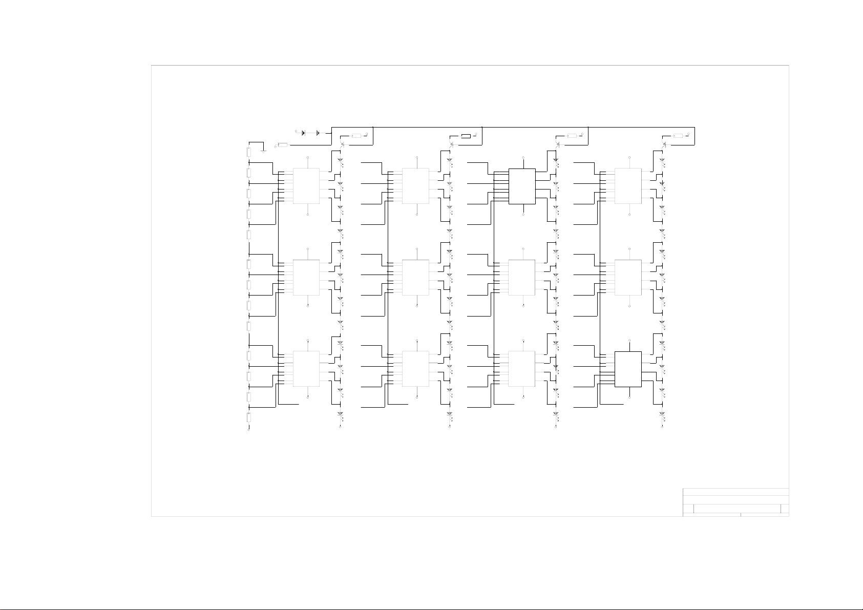
D1
V+
D2
1N4148
1N4148
0.4"R17
0.4"
BASEREF
22K
R3
270R
R4
75R
R6
120R
R7
180R
R8
270R
R9
360R
R10
510R
R11
820R
R12
1K
R13
1K5
R14
2K
R15
3K
R16
30K
V-
-21
-18
-15
-12
-9
-6
-3
0
+3
+6
+9
+12
5
4
7
6
9
8
11
10
5
4
7
6
9
8
11
10
5
4
7
6
9
8
11
10
METER1
LM2901
LM2901
LM2901
V+
3
2
+
O
+
V
1
O
+
14
+
O
13
+
O
-
-
V
12IC1
V-
V+
3
2
O
+
+
V
1
+
O
14
+
O
13
+
O
-
-
V
12IC2
V-
V+
3
2
+
O
+
V
1
+
O
14
+
O
13
+
O
-
-
V
12IC3
V-
V+
V+
R18
TR1
120R
BC212
AI
LED1
GRN
-21
LED2
-18
GRN
-15
LED3
GRN
-12
LED4
GRN
LED5
GRN
-9
LED6
-6
GRN
-3
LED7
GRN
0
LED8
YEL
LED9
YEL
+3
LED10
+6
YEL
+9
LED11
YEL
+12
LED12
RED
5
4
7
6
9
8
11
10
5
4
7
6
9
8
11
10
5
4
7
6
9
8
11
10
METER2
LM2901
LM2901
LM2901
V+
3
2
+
O
+
V
1
O
+
14
+
O
13
+
O
-
-
V
12IC4
V-
V+
3
2
O
+
+
V
1
+
O
14
+
O
13
+
O
-
-
V
12IC5
V-
V+
3
2
+
O
+
V
1
+
O
14
+
O
13
+
O
-
-
V
12IC6
V-
V-
V+
R19
TR2
120R
BC212
AI
LED13
GRN
-21
LED14
-18
GRN
-15
LED15
GRN
-12
LED16
GRN
LED17
GRN
-9
LED18
-6
GRN
-3
LED19
GRN
0
LED20
YEL
LED21
YEL
+3
LED22
+6
YEL
+9
LED23
YEL
+12
LED24
RED
METER3
V+
3
5
4
7
6
9
8
11
10
LM2901
2
+
O
+
V
1
O
+
14
+
O
13
+
O
-
-
V
12IC7
V-
V+
3
5
4
7
6
9
8
11
10
LM2901
2
O
+
+
V
1
+
O
14
+
O
13
+
O
-
-
V
12IC8
V-
V+
3
5
4
7
6
9
8
11
10
LM2901
2
+
O
+
V
1
+
O
14
+
O
13
+
O
-
-
V
12IC9
V-
V-
V+
R20
TR3
120R
BC212
AI
LED25
GRN
-21
LED26
-18
GRN
-15
LED27
GRN
-12
LED28
GRN
LED29
GRN
-9
LED30
-6
GRN
-3
LED31
GRN
0
LED32
YEL
LED33
YEL
+3
LED34
+6
YEL
+9
LED35
YEL
+12
LED36
RED
5
4
7
6
9
8
11
10
5
4
7
6
9
8
11
10
5
4
7
6
9
8
11
10
METER4
LM2901
LM2901
LM2901
V+
3
2
+
O
+
V
1
O
+
14
+
O
13
+
O
-
-
V
12IC10
V-
V+
3
2
O
+
+
V
1
+
O
14
+
O
13
+
O
-
-
V
12IC11
V-
V+
3
2
+
O
+
V
1
+
O
14
+
O
13
+
O
-
-
V
12IC12
V-
V-
V+
R21
TR4
120R
BC212
AI
LED37
GRN
LED38
GRN
LED39
GRN
LED40
GRN
LED41
GRN
LED42
GRN
LED43
GRN
LED44
YEL
LED45
YEL
LED46
YEL
LED47
YEL
LED48
RED
V-
Klark Teknik - DDA Division
Title
CS8 - LED OUTPUT MAIN
Size Document Number REV
C CD1311-1 A
Date: May 2, 1997 Sheet 2 of 3

V+
V+
CURRENT REF
5
4
7
6
9
8
11
10
5
4
7
6
9
8
11
10
5
4
7
6
9
8
11
10
METER5
LM2901
LM2901
LM2901
V+
3
2
+
O
+
V
1
+
O
14
+
O
13
+
O
-
-
V
12IC13
V-
V+
3
2
+
O
+
V
1
+
O
14
+
O
13
+
O
-
-
V
12IC14
V-
V+
3
2
+
O
+
V
1
+
O
14
+
O
13
+
O
-
-
V
12IC15
V-
-21
-18
-15
-12
-9
-6
-3
0
+3
+6
+9
+12
V+R22
TR5
120R
BC212
AI
LED49
GRN
-21
LED50
-18
GRN
-15
LED51
GRN
-12
LED52
GRN
LED53
GRN
-9
LED54
-6
GRN
-3
LED55
GRN
0
LED56
YEL
LED57
YEL
+3
LED58
+6
YEL
+9
LED59
YEL
+12
LED60
RED
5
4
7
6
9
8
11
10
5
4
7
6
9
8
11
10
5
4
7
6
9
8
11
10
METER6
LM2901
LM2901
LM2901
V+
3
2
+
O
+
V
1
+
O
14
+
O
13
+
O
-
-
V
12IC16
V-
V+
3
2
+
O
+
V
1
+
O
14
+
O
13
+
O
-
-
V
12IC17
V-
V+
3
2
+
O
+
V
1
+
O
14
+
O
13
+
O
-
-
V
12IC18
V-
R23
TR6
120R
BC212
AI
LED61
GRN
-21
LED62
-18
GRN
-15
LED63
GRN
-12
LED64
GRN
LED65
GRN
-9
LED66
-6
GRN
-3
LED67
GRN
0
LED68
YEL
LED69
YEL
+3
LED70
+6
YEL
+9
LED71
YEL
+12
LED72
RED
5
4
7
6
9
8
11
10
5
4
7
6
9
8
11
10
5
4
7
6
9
8
11
10
METER7
LM2901
LM2901
LM2901
V+
3
2
+
O
+
V
1
+
O
14
+
O
13
+
O
-
-
V
12IC19
V-
V+
3
2
+
O
+
V
1
+
O
14
+
O
13
+
O
-
-
V
12IC20
V-
V+
3
2
+
O
+
V
1
+
O
14
+
O
13
+
O
-
-
V
12IC21
V-
R24
TR7
120R
BC212
AI
LED73
GRN
-21
LED74
-18
GRN
-15
LED75
GRN
-12
LED76
GRN
LED77
GRN
-9
LED78
-6
GRN
-3
LED79
GRN
0
LED80
YEL
LED81
YEL
+3
LED82
+6
YEL
+9
LED83
YEL
+12
LED84
RED
5
4
7
6
9
8
11
10
5
4
7
6
9
8
11
10
5
4
7
6
9
8
11
10
METER8
LM2901
LM2901
LM2901
V+
3
2
+
O
+
V
1
+
O
14
+
O
13
+
O
-
-
V
12IC22
V-
V+
3
2
+
O
+
V
1
+
O
14
+
O
13
+
O
-
-
V
12IC23
V-
V+
3
2
+
O
+
V
1
+
O
14
+
O
13
+
O
-
-
V
12IC24
V-
V+R25
TR8
120R
BC212
AI
LED85
GRN
LED86
GRN
LED87
GRN
LED88
GRN
LED89
GRN
LED90
GRN
LED91
GRN
LED92
YEL
LED93
YEL
LED94
YEL
LED95
YEL
LED96
RED
V-V-V-V-
Klark Teknik - DDA Division
Title
CS8 - LED OUTPUT MAIN
Size Document Number REV
C CD1311-1 A
Date: May 2, 1997 Sheet 3 of 3
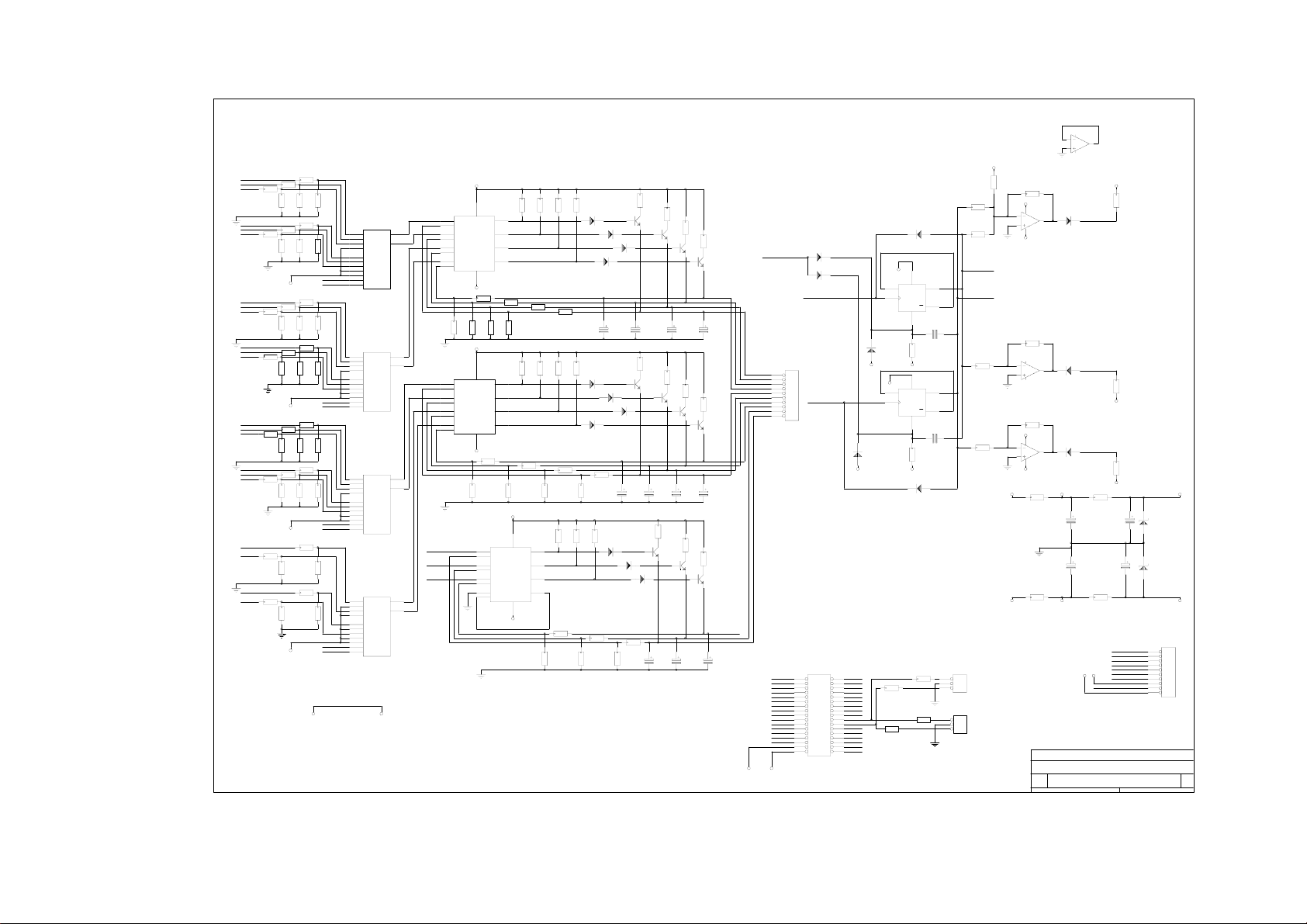
6
7
5
IC10B
D20
1N4148
TL072
D21
1N4148
D22
1N4148
V+
C14
220U
25V
C15
220U
25V
V-VIN-
CS8 LED O/P METER SUB PCB
TL072
AUXLED
MATLED
GRPLED
V+V-
V+
R109
22K
R110
22K
V-
R111
22K
V-
R69
360R
C16
220U
25V
0V
C17
220U
25V
R70
360R
GRPSW
AUXSW
MATSW
RECTR
GRPLED
AUXLED
MATLED
0V
VDD
D12
6V8
0.4"
D13
6V8
0.4"
VSS
CON3
1
2
3
4
5
6
7
8
9
10
10WAY
MHX
VDD
R3
R2
GP1
R1
MTX1
AUX1
GP2
MTX2
AUX2
GP3
MTX3
AUX3
GP4
MTX4
AUX4
GP5
MTX5
AUX5
GP6
MTX6
AUX6
GP7
AUX7
GP8
AUX8
10K
10K
R5
R4
4K7R64K7
4K7
R8
R7
10K
10K
R11
R10
4K7
4K7
VSS
R14
R13
10K
10K
R17
R16
4K7
4K7
R20
R19
10K
10K
R23
R22
4K7
4K7
VSS
R26
R25
10K
10K
R29
R28
4K7
4K7
R32
R31
10K
10K
R35
R34
4K7
4K7
VSS
R37
10K
R39
4K7
R41
10K
R43
4K7
VSS
10K
R9
10K
4K7
R15
10K
4K7
R21
10K
4K7
R27
10K
4K7
R33
10K
4K7
R38
10K
4K7
R42
10K
4K7
12
14
15
11
R12
1
5
2
4
6
10
Q1
9
Q2
R18
12
14
15
11
R24
1
5
2
4
6
10
Q1
9
Q2
R30
12
14
15
11
R36
1
5
2
4
6
10
Q1
9
Q2
R40
12
14
15
11
1
R44
5
2
4
6
10
Q1
9
Q2
VSS VEE
IC1
13
X0
X
X1
3
X2
Y
X3
Y0
Y1
Y2
Y3
INH
A
B
4052
IC2
13
X0
X
X1
3
X2
Y
X3
Y0
Y1
Y2
Y3
INH
A
B
4052
IC3
13
X0
X
X1
3
X2
Y
X3
Y0
Y1
Y2
Y3
INH
A
B
4052
IC4
13
X
X0
X1
3
Y
X2
X3
Y0
Y1
Y2
Y3
INH
A
B
4052
V+
3
5
+
+
4
V
-
7
+
6
-
9
+
8
-
11
+
-
10
-
V
12IC5
LM2901
V-
R90
R91
R89
75K
75K
75K
V+
3
5
+
+
4
V
-
7
+
6
-
9
+
8
-
11
+
-
10
-
V
12IC6
LM2901
V-
R57
75K
5
MIXL
4
7
MIXC
6
9
MIXR
8
11
10
LM2901
R46
R47
R45
33K
2
O
1
O
14
O
13
O
R85
R86
150K
150K
R92
75K
R53
2
33K
O
1
O
14
O
13
O
R97
150K
R58
75K
V+
3
+
+
V
+
+
+
-
-
V
12IC7
V-
R48
33K
33K
33K
1N4148
R87
R88
150K
150K
R54
R55
R56
33K
33K
33K
R99
R98
150K
150K
R59
R60
75K
75K
R62
R61
2
33K
33K
33K
O
1
O
14
O
13
O
R104
1K
R64
R65
220K
220K
R81
1K5
R82
D3
D9
1N4148
0.4"
R66
1N4148
1N4148
0.4"
0.4"
D2
C2
2U2
63V0.2
R93
1K5
D6
0.4"
0.4" D11
1K
2U2
63V0.2
1N4148
R106
2U2
63V0.2
1K5
R83
TR1
1K5
BC182
AI
BC182
TR5
BC182
AI
BC182
C6
R101
1K5
D10
0.4"
C11
R84
TR2
1K5
TR3
AI
AI
BC182
TR4
BC182
AI
METER4 AUXSW
METER3
METER2
METER1
C3
C4
2U2
2U2
63V0.2
63V0.2
R94
1K5
R95
1K5
R96
TR6
1K5
TR7
AI
BC182
TR8
BC182
AI
AI
METER8
METER7
METER6
METER5
C7
C8
2U2
2U2
63V0.2
63V0.2
R102
1K5
R103
TR9
1K5
BC182
AI
TR10
BC182
TR11
AI
BC182
AI
RECTR
RECTC
RECTL
C13
C12
2U2
2U2
63V0.2
63V0.2
GRPSW
VIN- VIN+
D14
1N4148
D15
1N4148
CON2
1
2
3
4
5
6
MATSW
7
8
9
10
10WAY
MHX
D17
1N4148
VSS VSS
CON1
12
34
56
78
910
11 12
13 14
15 16
17 18
19 20
21 22
23 24
25 26
27 28
29 30
31 32
33 34
34WAY
IDCMD
MIXL
MIXC
MTX1
AUX3
0V
GP2
MTX3
AUX5
GP4
-V
+V
MTX5
AUX7
GP6
GP7
0V
GP8
MIXR
AUX1
AUX2
GP1
-V
+V
MTX2
AUX4
GP3
MTX4
0V
AUX6
GP5
MTX6
AUX8
-V
+V
1N4148
D18
1N4148
VSS
IC8A
6
5
1
D
Q
S
3
CLK
2
Q
R
4013
4
C18
220N
R71
D16
100K
VSSVSS
IC8B
8
VSS
9
13
D
Q
S
11
CLK
12
Q
R
4013
1
0
C19
220N
R72
100K
D19
1N4148
CON5
R113
WW-4W
WW-4W
1
2
22R
3
3WAY
METWAY
R107
CON4
1
2
22R
3
3WAY
METWAY
R112
22R
WW-4W
R108
22R
WW-4W
D4
0.4"
1N4148
D1
1N4148
0.4"
C1
2U2
63V0.2
D5
1N4148
0.4"
1N4148
0.4" D7
D8
1N4148
0.4"
R100
150K
C5
2U2
63V0.2
R63
1N4148
R105
1K
220K
GROUP
R73
10K
10K
R75
10K
R77
10K
R79
10K
R76
22K
V-R74
4
IC9A
2
1
3
8
V+
Q2
Q1
AUX
R78
22K
IC9B
6
7
5
TL072
MATRIX
R80
22K
V-
4
IC10A
2
1
3
TL072
8
V+
VIN+
R67
1R
R68
1R
DDA, HOUNSLOW, MIDDX, TW3 2EB, ENGLAND.
Title
Size Document Number REV
C CD1312-1 A
Date: March 18, 1997 Sheet 1 of 1

2WAY
WIR
CON9S
1
2
AUXLED-S
R17
2K2
GROUP
TP2301
AUX
TP2301
2
4
6
8
10
12
14
16
LED2
2
4
6
8
10
12
14
16
LEDBLK-RED
2
4
6
8
10
12
14
16
LEDBLK-RED
SW1
TP2301
MATRIX
SW2
R2
100K
SW3
100K
LED1
R14
2K2
LED3
AUXLED-S
C1
47N
LEDBLK-RED
1
3
5
7
9
11
13
15
CON8S
R11
2K2
2WAY
1
WIR
3
5
7
9
11
13
15
1
3
5
7
9
11
13
15
CON5S
1
2
2WAY
WIR
VSSS
CON6S
1
2
2WAY
WIR
VSSS
R5
CON7S
1
2
2WAY
WIR
+V
CON11
METWAY
SUPPLY
D7
1N4148
S
R
VSSVSS
S
R
R100
22R
WW-4W
1
2
3
3WAY
LITTLITE
R101
22R
WW-4W
IC1A
6
1
Q
2
Q
4013
4
C6
47N
IC1B
8
13
Q
12
Q
4013
1
0
C7
47N
D8
1N4148
R110
22R
3WAY
METWAY
CON3
1
2
3
D4
1N4148
1N4148
WW-4W
LITTLITE
R111
22R
WW-4W
VSS
5
D
3
CLK
R3
D3
100K
VSS
9
D
11
CLK
R6
100K
MIX METER SUPPLY
2WAY
2WAY
2WAY
2WAY
AUXLED
R97
100R
WW-4W
-V
VIN-
CON8
1
2
ML
MTXLED
VDD
CON5
D1
1
2
1N4148
ML
D2
1N4148
R1
1K
C2
47N
CON6
ML
CON7
ML
VSS
1
2
R4
1K
C3
47N
1
2
VSS
VSS VSS
1
2
CON10
METWAY
SUPPLY
R108
10R
METER 1-8
SUPPLY
CON4
1
1
2
2
3
3
3WAY
3WAY
METWAY
R109
10R
VDD
R7
10K
R8
10K
R9
10K
MATRIX
R12
6
10K
5
R15
6
10K
5
VIN+
VIN-
GROUP
VIN-
2
3
VIN+
R13
22K
IC11B
AUX
R16
22K
IC12B
R98
VDD
360R
C4
C8
220U
220U
25V
25V
0V
C9
C5
220U
220U
25V
25V
R99
360R
R10
R105
22K
22K
4
IC12A
D9
1
1N4148
TL072
8
D10
7
1N4148
TL072
D11
7
1N4148
TL072
VIN-
GP1
MTX1
AUX1
D5
6V8
0.4"
GP2
MTX2
D6
AUX2
6V8
0.4"
VSS
VIN+
GP3
MTX3
AUX3
CON9
1
2
2WAY
ML
VIN+
GP4
MTX4
AUX4
GP5
MTX5
AUX5
GP6
MTX6
AUX6
MTXLED
R106
22K
VIN-
GP7
AUX7
AUXLED
R107
22K
GP8
AUX8
VSS
R20
R19
R18
10K
10K
10K
R22
R23
R21
4K7
4K7
4K7
R26
R25
R24
10K
10K
10K
R28
R29
R27
4K7
4K7
4K7
R32
R31
R30
10K
10K
10K
R34
R35
R33
4K7
4K7
4K7
R38
R37
R36
10K
10K
10K
R40
R41
R39
4K7
4K7
4K7
R44
R43
R42
10K
10K
10K
R46
R47
R45
4K7
4K7
4K7
R50
R49
R48
10K
10K
10K
R52
R53
R51
4K7
4K7
4K7
R55
R54
10K
10K
R58
R57
R56
4K7
4K7
4K7
R60
R59
10K
10K
R63
R62
R61
4K7
4K7
4K7
VEE
IC2
12
X0
X
14
X1
15
X2
Y
11
X3
1
Y0
5
Y1
2
Y2
4
Y3
6
INH
10
A
9
B
4052
VSS
IC3
12
X0
X
14
X1
15
X2
Y
11
X3
1
Y0
5
Y1
2
Y2
4
Y3
6
INH
10
A
9
B
4052
VSS
IC4
12
X0
X
14
X1
15
X2
Y
11
X3
1
Y0
5
Y1
2
Y2
4
Y3
6
INH
10
A
9
B
4052
VSS 5
IC5
12
X
X0
14
X1
15
Y
X2
11
X3
1
Y0
5
Y1
2
Y2
4
Y3
6
INH
10
A
9
B
4052
VSS
1/4
PR1
R64
5K
15K
VIN-
4
IC6A
2
13
3
13
3
13
3
13
3
3
R65
75R
1/4
PR3
5K
2
3
R71
75R
1/4
PR5
5K
2
3
R77
75R
1/4
PR7
5K
2
3
R83
75R
1/4
PR8
5K
6
5
R86
75R
R66
1
8
TL072
VIN+
R68
75R
R70
15K
VIN-
4
IC7A
1
TL072
8
VIN+
1/4
PR4
5K
R74
75R
R76
15K
VIN-
4
IC8A
1
8
TL072
VIN+
1/4
PR6
5K
R80
75R
R82
15K
VIN-
4
IC9A
1
8
TL072
VIN+
R85
15K
IC9B
7
TL072
METER1
3K6
1/4
PR2
5K
R67
15K
IC6B
6
5
6
5
6
R69
7
3K6
TL072
R72
METER3
3K6
R73
15K
IC7B
R75
7
3K6
TL072
R78
METER5
3K6
R79
15K
IC8B
R81
7
3K6
TL072
R84
METER7
3K6
R87
METER8
3K6
METER6
LAST C
LAST CON
LAST D
LAST LED
LAST IC
LAST SW
LAST R
LAST PR
METER2
MIXL
MIXC
MIXRMETER4
C9
CON11
D11
LED3
IC12
SW3
R111
PR11
1/4
PR9
R102
4K7
R103
4K7
R92
75R
R104
4K7
R95
75R
MIXR
AUX1
AUX2
GP1
-V
+V
MTX2
AUX4
GP3
MTX4
0V
AUX6
GP5
MTX6
AUX8
-V
+V
0V
0V
0V
0V
0V
0V
0V
0V
0V
0V
0V
0V
0V
DDA
UNIT 1,WHITTON RD, HOUNSLOW
Title
Size Document Number REV
C CD1310-1 A
Date: March 17, 1997 Sheet of
R88
5K
4K7
VIN-
4
IC10A
2
3
R89
VIN+
75R
1/4
PR10
5K
IC10B
6
5
1/4
PR11
5K
VIN-
4
IC11A
2
3
8
VIN+
CON1
12
34
56
78
910
11 12
13 14
15 16
17 18
19 20
21 22
23 24
25 26
27 28
29 30
31 32
33 34
34WAY
IDCMD
CON2
12
34
56
78
910
11 12
13 14
15 16
17 18
19 20
21 22
23 24
25 26
26WAY
IDCMD
CS8 VU METER
R90
1
8
TL072
R91
4K7
7
TL072
R94
4K7
1
TL072
MIXL
MIXC
MTX1
AUX3
0V
GP2
MTX3
AUX5
GP4
-V
+V
MTX5
AUX7
GP6
GP7
0V
GP8
METERL
3K6
R93
METERC
3K6
R96
METERR
3K6
0V
METER1
METER2
METER3
METER4
METER5
METER6
METER7
METER8
METERL
METERC
METERR
0V
SIG1
SIG3
SIG5
SIG7
SIG9
SIG11
SIG13
SIG15
SIG17
SIG19
SIG21
SIG23
CON1
12
34
56
78
910
11 12
13 14
15 16
17 18
19 20
21 22
23 24
25 26
26WAY
IDCMD
SIG2
SIG4
SIG6
SIG8
SIG10
SIG12
SIG14
SIG16
SIG18
SIG20
SIG22
SIG24
INPUT 1-24
SIG1
SIG3
SIG5
SIG7
-V
+V
SIG10
SIG12
SIG14
SIG16
0V
SIG17
SIG19
SIG21
SIG23
-V
+V
CON2
12
34
56
78
910
11 12
13 14
15 16
17 18
19 20
21 22
23 24
25 26
27 28
29 30
31 32
33 34
34WY
IDCBXR
SIG2
SIG4
SIG6
SIG8
0V
SIG9
SIG11
SIG13
SIG15
-V
+V
SIG18
SIG20
SIG22
SIG24
0V
MIXR
AUX1
AUX2
GP1
MTX2
AUX4
GP3
MTX4
AUX6
GP5
MTX6
AUX8
GP8
CON5
12
34
56
78
910
11 12
13 14
15 16
17 18
19 20
21 22
23 24
25 26
26WAY
IDCMD
MIXL MIXR
MIXC
MTX1
AUX3
GP2
MTX3
AUX5
GP4
MTX5
AUX7
GP6
GP7
OUTPUT & MASTERS
CON6
AUX1
AUX2
GP1
-V
+V
MTX2
AUX4
GP3
MTX4
0V
AUX6
GP5
MTX6
AUX8
-V
+V GP8
12
34
56
78
910
11 12
13 14
15 16
17 18
19 20
21 22
23 24
25 26
27 28
29 30
31 32
33 34
34WY
IDCBXR
MIXL
MIXC
MTX1
AUX3
0V
GP2
MTX3
AUX5
GP4
-V
+V
MTX5
AUX7
GP6
GP7
0V
SIG25
SIG27
SIG29
SIG31
SIG33
SIG35
SIG37
SIG39
SIG41
SIG43
SIG45
SIG47
CON3
12
34
56
78
910
11 12
13 14
15 16
17 18
19 20
21 22
23 24
25 26
26WAY
IDCMD
SIG26
SIG28
SIG30
SIG32
SIG34
SIG36-V+V
SIG38
SIG40
SIG42
SIG44
SIG46
SIG48
INPUT 25-48
SIG25
SIG27
SIG29
SIG31
SIG34
SIG36
SIG38
SIG40
0V
SIG41
SIG43
SIG45
SIG47
-V
+V
CON4
12
34
56
78
910
11 12
13 14
15 16
17 18
19 20
21 22
23 24
25 26
27 28
29 30
31 32
33 34
34WY
IDCBXR
SIG26
SIG28
SIG30
SIG32
0V
SIG33
SIG35
SIG37
SIG39
-V
+V
SIG42
SIG44
SIG46
SIG48
0V
CON7
1
2
3
3WAY
MH156
DDA, HOUNSLOW, MIDDX, TW3 2EB, ENGLAND.
Title
Size Document Number REV
B CD1309-1 A
Date: February 13, 1997 Sheet 1 of 1
+V
0V
-V
CS8 METERS CONNECTOR
 Loading...