

Page 1
P112 Single Board Computer
Assembly and Operation Manual
Revision 1.1
David Griffith
Wednesday May 10, 2006
1
Page 2

This page is intentionally left blank.
2
Page 3

Contents
1 Introduction 4
1.1 What is this thing? . . . . . . . . . . . . . . . . . . . . . . . . . . 4
1.2 What do I need to know? . . . . . . . . . . . . . . . . . . . . . . 4
1.3 What’s in this kit? . . . . . . . . . . . . . . . . . . . . . . . . . . 4
1.4 What’s not in this kit? . . . . . . . . . . . . . . . . . . . . . . . . 5
2 Cables and Components 7
2.1 Cables . . . . . . . . . . . . . . . . . . . . . . . . . . . . . . . . . 7
2.1.1 Power Cable . . . . . . . . . . . . . . . . . . . . . . . . . 7
2.1.2 Terminal Cable . . . . . . . . . . . . . . . . . . . . . . . . 7
2.1.3 Disk Drive Cable . . . . . . . . . . . . . . . . . . . . . . . 8
2.1.4 Parallel Port Cable . . . . . . . . . . . . . . . . . . . . . . 8
2.2 Complete List of Parts . . . . . . . . . . . . . . . . . . . . . . . . 9
3 Construction 11
3.1 Before Anything Else . . . . . . . . . . . . . . . . . . . . . . . . . 11
3.2 Getting Started . . . . . . . . . . . . . . . . . . . . . . . . . . . . 11
3.3 Soldering the First Parts . . . . . . . . . . . . . . . . . . . . . . . 12
3.4 Soldering Everything Else . . . . . . . . . . . . . . . . . . . . . . 12
4 Setting Up 14
4.1 Jumper Settings . . . . . . . . . . . . . . . . . . . . . . . . . . . 14
4.2 Terminal Settings . . . . . . . . . . . . . . . . . . . . . . . . . . . 15
4.3 Disk Drives . . . . . . . . . . . . . . . . . . . . . . . . . . . . . . 15
4.4 Powering Up . . . . . . . . . . . . . . . . . . . . . . . . . . . . . 16
5 Debugger 18
5.1 Help Function . . . . . . . . . . . . . . . . . . . . . . . . . . . . . 18
5.2 Set Breakpoint . . . . . . . . . . . . . . . . . . . . . . . . . . . . 19
5.3 Display / Set Memory . . . . . . . . . . . . . . . . . . . . . . . . 19
5.4 Go (Run Program) . . . . . . . . . . . . . . . . . . . . . . . . . . 20
5.5 Trace instructions . . . . . . . . . . . . . . . . . . . . . . . . . . 20
5.6 Display / Set Registers . . . . . . . . . . . . . . . . . . . . . . . . 21
5.7 Loading Files . . . . . . . . . . . . . . . . . . . . . . . . . . . . . 21
5.8 Input from Port . . . . . . . . . . . . . . . . . . . . . . . . . . . . 22
5.9 Output to Port . . . . . . . . . . . . . . . . . . . . . . . . . . . . 22
5.10 System Boot . . . . . . . . . . . . . . . . . . . . . . . . . . . . . 22
5.11 Load OS and return to DEBUG . . . . . . . . . . . . . . . . . . 22
5.12 DS-1302 RAM Parameters . . . . . . . . . . . . . . . . . . . . . . 23
6 Troubleshooting 25
6.1 Stone Dead . . . . . . . . . . . . . . . . . . . . . . . . . . . . . . 25
6.2 Garbaged Sign-on Message . . . . . . . . . . . . . . . . . . . . . 25
6.3 Disk Drive Won’t Work . . . . . . . . . . . . . . . . . . . . . . . 25
3
Page 4

6.4 An Example . . . . . . . . . . . . . . . . . . . . . . . . . . . . . . 27
7 Logic Description 28
7.1 CPU . . . . . . . . . . . . . . . . . . . . . . . . . . . . . . . . . . 28
7.1.1 Serial Port . . . . . . . . . . . . . . . . . . . . . . . . . . 28
7.1.2 Parallel Port . . . . . . . . . . . . . . . . . . . . . . . . . 29
7.1.3 DMA . . . . . . . . . . . . . . . . . . . . . . . . . . . . . 29
7.1.4 Memory Mapping . . . . . . . . . . . . . . . . . . . . . . 29
7.2 Memory . . . . . . . . . . . . . . . . . . . . . . . . . . . . . . . . 30
7.2.1 ROM . . . . . . . . . . . . . . . . . . . . . . . . . . . . . 30
7.2.2 On-Board RAM . . . . . . . . . . . . . . . . . . . . . . . 31
7.2.3 Expansion RAM . . . . . . . . . . . . . . . . . . . . . . . 31
7.3 IO Cycle Control . . . . . . . . . . . . . . . . . . . . . . . . . . . 31
7.4 Real-Time Clock . . . . . . . . . . . . . . . . . . . . . . . . . . . 31
7.5 Expansion Socket . . . . . . . . . . . . . . . . . . . . . . . . . . . 32
7.6 Multi-I/O Chip . . . . . . . . . . . . . . . . . . . . . . . . . . . . 32
7.6.1 Address Decoding . . . . . . . . . . . . . . . . . . . . . . 32
7.6.2 Cycle Timing . . . . . . . . . . . . . . . . . . . . . . . . . 32
7.6.3 Safety Latch . . . . . . . . . . . . . . . . . . . . . . . . . 32
7.7 Serial Port 2 . . . . . . . . . . . . . . . . . . . . . . . . . . . . . 33
7.8 Diskette Port . . . . . . . . . . . . . . . . . . . . . . . . . . . . . 33
7.9 Printer Port . . . . . . . . . . . . . . . . . . . . . . . . . . . . . . 33
8 Major Components 34
8.1 CPU Chip . . . . . . . . . . . . . . . . . . . . . . . . . . . . . . . 34
8.2 I/O Combination . . . . . . . . . . . . . . . . . . . . . . . . . . . 34
8.2.1 Port Addressing . . . . . . . . . . . . . . . . . . . . . . . 34
8.3 Flash ROM . . . . . . . . . . . . . . . . . . . . . . . . . . . . . . 35
8.4 Realtime Clock . . . . . . . . . . . . . . . . . . . . . . . . . . . . 35
9 Connector Pins 36
9.1 P1 — RAM Size Selector . . . . . . . . . . . . . . . . . . . . . . 36
9.2 P2 — DMA Requests . . . . . . . . . . . . . . . . . . . . . . . . 36
9.3 P3 — Flash Bootload Selector . . . . . . . . . . . . . . . . . . . . 36
9.4 P4 — Serial Port 1 . . . . . . . . . . . . . . . . . . . . . . . . . . 38
9.5 P5 — SYNC Jumper . . . . . . . . . . . . . . . . . . . . . . . . . 38
9.6 P6 — Power Supply / Reset . . . . . . . . . . . . . . . . . . . . . 39
9.7 P7 — Parallel Printer . . . . . . . . . . . . . . . . . . . . . . . . 39
9.8 P8 — Serial Port 2 . . . . . . . . . . . . . . . . . . . . . . . . . . 40
9.9 P9 — Disk Drives 0 and 1 . . . . . . . . . . . . . . . . . . . . . . 41
9.10 P10 — Disk Drives 2 and 3 . . . . . . . . . . . . . . . . . . . . . 41
9.11 P11 – Battery Isolator . . . . . . . . . . . . . . . . . . . . . . . . 41
9.12 P12 — ROM Pin-3 Function . . . . . . . . . . . . . . . . . . . . 42
9.13 P13 — RAM Pin-30 Function . . . . . . . . . . . . . . . . . . . . 42
9.14 P14 — Extra Serial Ports . . . . . . . . . . . . . . . . . . . . . . 42
9.15 J1 — Bus Expansion . . . . . . . . . . . . . . . . . . . . . . . . . 45
4
Page 5

10 Software 47
10.1 Z System and ZSDOS . . . . . . . . . . . . . . . . . . . . . . . . 47
10.2 Flash Programmer . . . . . . . . . . . . . . . . . . . . . . . . . . 48
10.3 DISKCOPY . . . . . . . . . . . . . . . . . . . . . . . . . . . . . . 48
11 Warranty, Etc. 49
5
Page 6

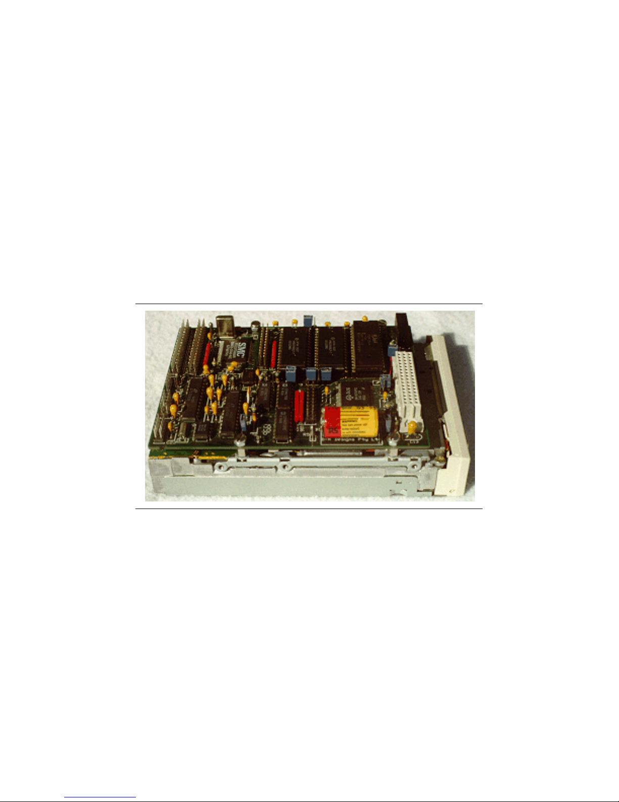
1 Introduction
1.1 What is this thing?
This document provides detailed illustrated instructions on building and using
the P112 single board computer. This board has the footprint of a typical 3.5”
floppy drive and may be mounted on the underside of one. Its CPU is a Zilog
Z180 (an enhanced version of the venerable Z80). A multifunction I/O chip
provides serial ports, a parallel port, and support for up to four floppy drives.
A terminal, or at least a null-modem cable connected to another computer
running a terminal-emulator is required to communicate with the P112.
The P112 was designed by David Brooks in 1996. He sold boards with the
five surface-mount comp onents preinstalled for about a year, then stopped due
to lack of demand. Since then, the P112 has gained a reputation as a welldesigned machine for running CP/M and similar operating systems. In late
2004, in response to growing interest in the P112 board, another run of boards
was produced by David Griffith. After a lot of work, unexpected problems, and
gnashing of teeth, kits started to ship in late 2005.
Most of the content of this manual is taken directly and usually verbatim from
two PDF files produced by David Brooks in 1996 as documentation for the first
run of P112 boards. Other content comes from documentation from related
utilities written specifically for the P112.
This introduction, assembly instructions, software documentation, and photographs were created by David Griffith.
1.2 What do I need to know?
You should know the basics of soldering. Because of the small size of this board
and certain delicate parts, I do not reccomend this as for a first soldering project.
Get a little project kit from Jameco and practice there first.
1.3 What’s in this kit?
In this kit you will find the following:
One four-layer printed circuit board
A four-layer circuit board is not something one can easily make in the
garage. This board has two surface-mount chips (the CPU and the IO
controller) and some discrete devices already mounted. Since there was
no way around having those surface-mount parts, that part has been done
for you.
6
Page 7

One set of electronic components
All the hard work of finding these components at good prices has already
been done for you.
One 3.5” floppy disk
This is a ZSDOS boot disk created by Terry Gulczynski specifically for
this new run of P112 boards. The boot disk supplied by David Brooks
with the first run of P112 boards will still work, but is discouraged.
One copy of the Walnut Creek CP/M CDROM
This CD dated November 1994 contains assorted utilities, games, system
software, source code, and other things for computers running CP/M or
similar operating systems. It has long been out of print and Walnut Creek
has said that no permission is needed to reproduce it.
One documentation CDROM
This CD contains the new P112 documentation (which you are now reading) and lots of other goodies like more utilities, operating systems, languages, and so on. A lot of stuff gathered by Rlee Peters is also included.
This CD is not documented in this manual.
1.4 What’s not in this kit?
This kit doesn’t include things that can be found at a typical consumer electronics parts shop. Other things you might want to complete this project can
be easily found on auction websites like Ebay. You might also have much of
these things already.
Soldering equipment All of these soldering items can be found at Radio
Shack (http://www.radioshack.com/).
A soldering iron drawing 15 to 30 watts is plenty powerful for this job.
Don’t go any higher or else you’ll risk damage to the board and/or components. Make sure you have a narrow tip. One of those cylindrical tips that
you sharpen to a point with a file will work, but will be very frustrating
to use when mounting the expansion connector.
Plain old 60/40 solder of .032” or .064” (.6mm to 1.2mm) is good. If you
prefer 63/37, that’s good too. Make sure you get rosin-core solder. Acid
core solder will ruin electronics. A solder of 96% tin and 4% silver is a
good choice of lead-free s older, but is more expe nsive. Two ounces (about
50 grams) of solder will be plenty.
It may be necessary to flux the board. I needed it. Others have reported
that it’s not necessary. You’ll know if you need it if molten solder will
not wet the connection you’re trying to solder. The type of flux is not
7
Page 8

particularly imp ortant. Just make sure it’s okay for electronics use and
you have the correct flux rem over. Radio Shack stocks suitable paste flux
and flux remover.
Picks, tweezers, and brushes will be handy.
Desoldering braid is essential for cleaning up mistakes. Don’t fool yourself
into thinking you won’t make any mistakes.
Grounding strap This is also available at Radio Shack. This device is essen-
tial to prevent static electricity damage to chips.
Chip puller and inserter This is also available at Radio Shack. They are
frequently included in “computer tool kits”.
Chip pin straightener You may or may not need one, but it’s a good idea to
have one just in case. They sometimes can be found at Radio Shack. The
Jameco part number is #99362. Mouser doesn’t appear to carry it.
Serial terminal You’ll need some way to talk to your new computer. A
second-hand dumb terminal found on Ebay (http://www.ebay.com) will
serve you well. Make sure you also get the correct cables. A null modem
adapter may be necessary.
Null modem cable or null modem adapter If you can’t get a terminal,
you can use a null mo dem cable and a terminal emulator program.
Floppy drives You’ll need at least one floppy drive. Two is nicer. You can
have as many as four, but two drives is best. This board can use any
internal 34-pin-interface floppy drive that an x86 PC can. Purists might
want to use 5.25” drives. 5.25” disks can be a bit hard to find, but it
shouldn’t be a big problem. Since this kit includes only 3.5” disks, use
3.5” drives unless you know what you’re doing. If you really know what
you’re doing and know where to look, you can use those big 8” floppies.
Chassis You’ll probably want a case to put your computer in when you’re
finished. Radio Shack carries a small variety of cases that might suit you.
A better choice may be to get an old external hard drive case.
Power supply This computer draws about 150 milliamps not including the
floppy drives. Even the tiniest computer power supply should work fine.
If you mount your computer in an old hard drive case, chances are that
you’ll have a good power supply too.
Mounting hardware and tools I can’t anticipate what situations that may
arise when mounting your computer. A computer shop or Radio Shack
will be helpful. You’ll have to look at how you want to mount the board
and what you’ll need to do it. If you want to mount it to the underside
of a floppy drive, you’ll need some standoffs and screws.
8
Page 9
2 Cables and Components
9 8 7 6 5 4 3 2 1
1
2
3
4
5
6
7
8
9
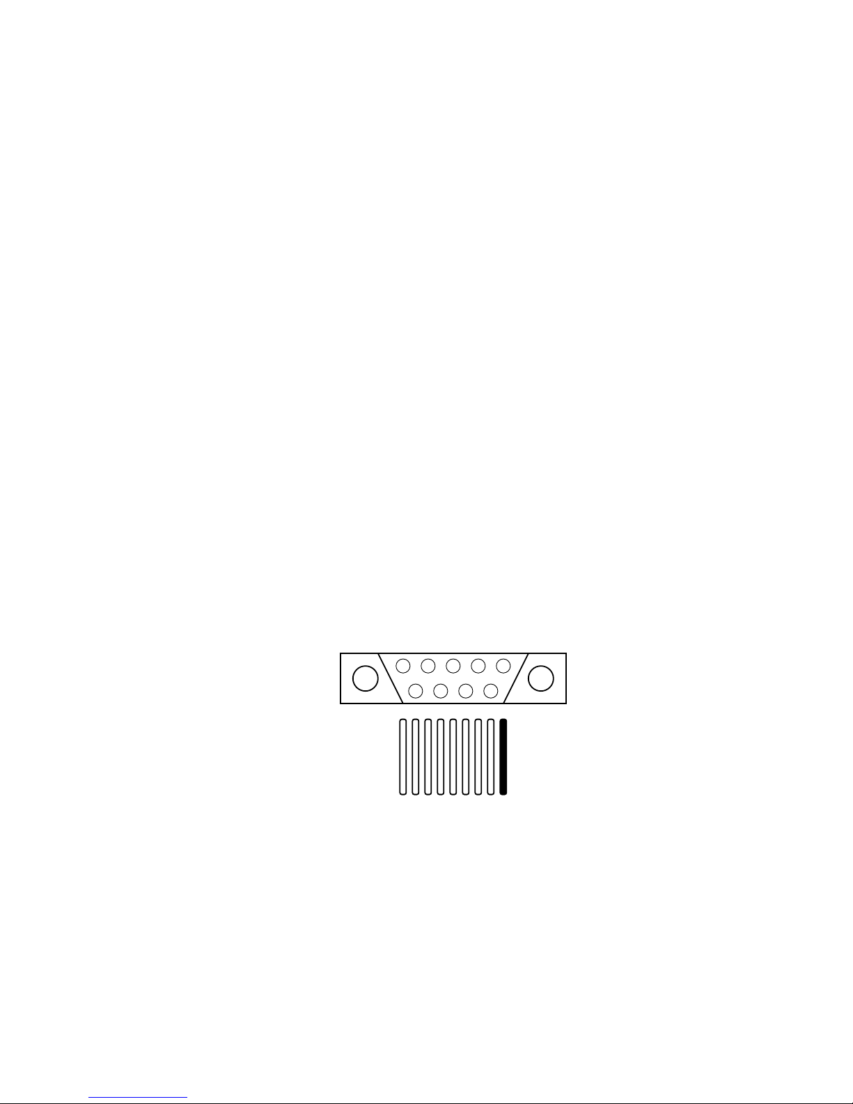
Serial connector wired straight through (solder side view).
2.1 Cables
All the basic I/O connections are at the left edge of the PCB. You will need the
following cables to run the board:
2.1.1 Power Cable
Connects to P6. Reading from top to bottom the pins are
GND
VDD
Reset
VDD
GND
The Reset pin may be left unconnected (it has a pull-up). To force a reset, pull
this line low.
Nominal power consumption (PCB only) is 150mA at 5V.
2.1.2 Terminal Cable
RS-232 terminals may be c onnected to P4 and P8 with the primary terminal
being at P4. A 10-conductor ribbon cable connects via a standard IDC socket
to the board. The tenth conductor is clipped off and the rest are crimped or
soldered to a standard IDC DB-9 plug as follows:
This generates the same pinout as a 9-pin serial port found on a typical x86 PC.
Two cables wired like this have been provided in your kit of parts. Depending
on how your terminal’s serial port is wired, you may need a null modem cable
or adapter.
9
Page 10
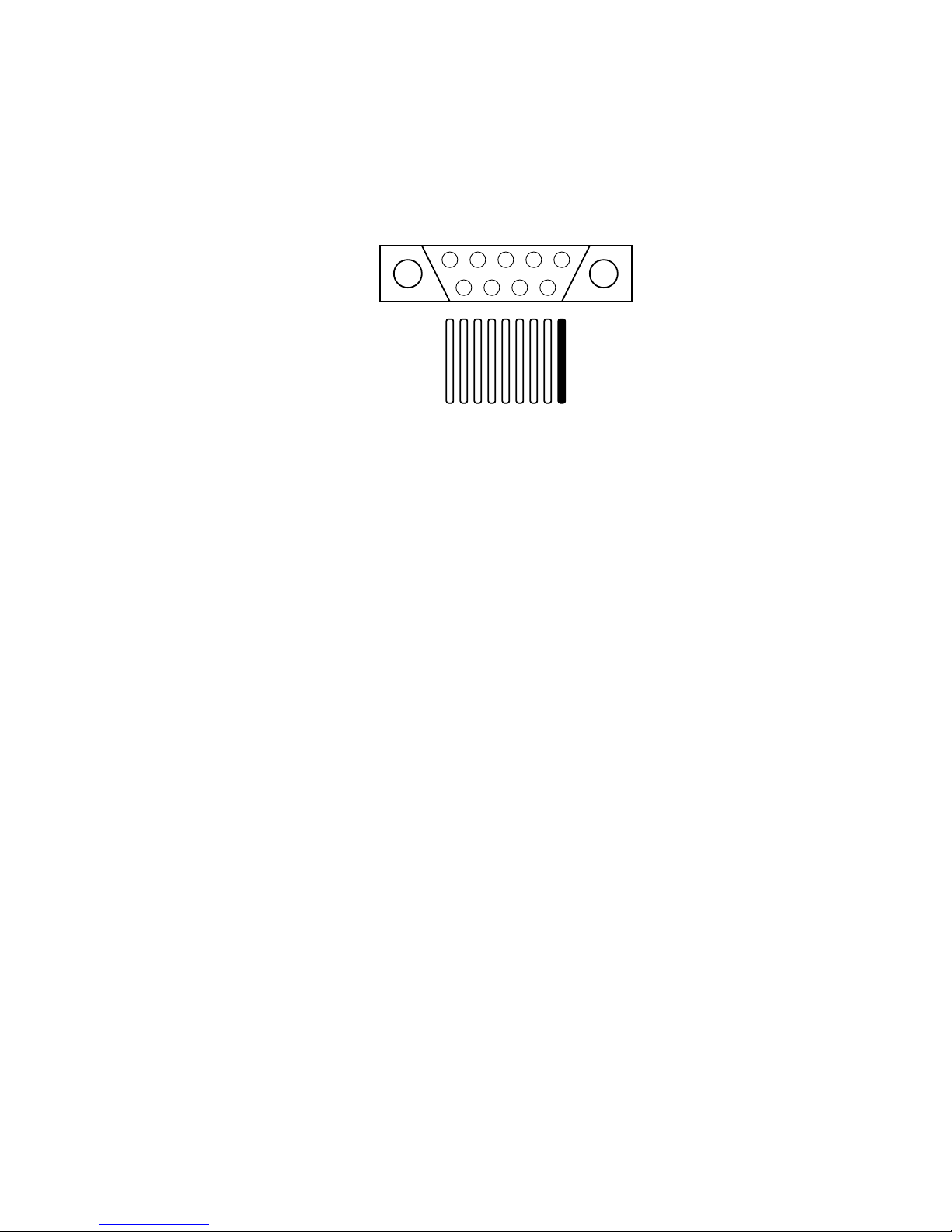
If you want to eliminate the need for an external null modem adapter, unscrew
9 8 7 6 5 4 3 2 1
1
8
972 345
6
Serial connector with null modem crossovers (solder side view).
the jack screws and rewire the pigtail as follows:
This will allow you to connect the P112 to an x86-style serial port with a cable
wired straight through. Again, depending on your terminal, you may be able
to use a standard 9-to-25-pin modem cable to connect the P112 to a standard
serial terminal.
2.1.3 Disk Drive Cable
This is wired as for a PC-AT, ie a direct 34-way connection from P9 or P10 to
the first drive, then cores 10-16 reversed in the path to the 2nd drive. In P9, the
first drive will be Drive 0, and the second Drive 1. From P10, they are Drives
3 and 2 similarly (note the reversed assignment).
In other words, a standard floppy ribbon cable is what you need. This cable is
not included. Sorry, I couldn’t find enough in large quantities.
2.1.4 Parallel Port Cable
A standard 26-way IDC receptacle fits the board. Clip off core 26 of the cable,
and run the others to a DB-25 socket (Pin-1 to Pin-1). This generates a standard
PC-type printer interface.
This sort of cable is identical to the provided terminal cables. Unfortunately, I
was unable to find any of these pre-made, so one is not included in the kit of
parts.
10
Page 11
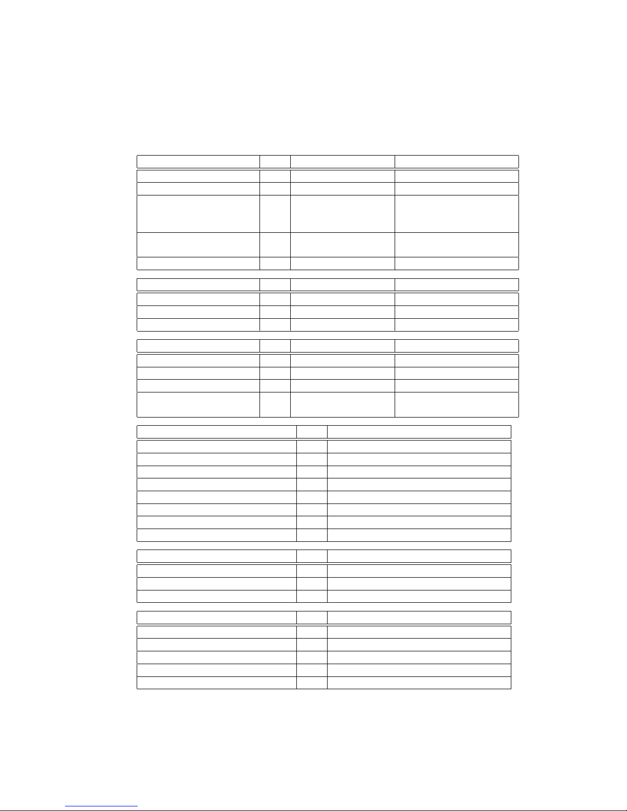
2.2 Complete List of Parts
Capacitors Qty. Markings Location
22ρF ceramic 4 220k (blue) C1 C2 C25 C26
120ρF ceramic 1 121 J5A (blue) C12
.1µF bypass 14 104 CSR (tan) C3 C15 C16 C17 C18
C19 C20 C21 C22 C23
C24 C28 C29 C30
1µF, 16V tantalum 9 1 C4 C5 C6 C7 C8
C9 C10 C11 C27
22µF, 10V tantalum 2 22µ C13 C14
Resistor Packs Qty. Markings Locations
7x220 Ω
7x2.2k Ω 1 8A222G U14
7x47k Ω 2 8A473G U16 U17
Resistors Qty. Markings Location
4.7k Ω 3 yellow-violet-red R3 R4 R11
10k Ω 3 brown-black-orange R5 R7 R10
27k Ω 1 red-violet-orange R9
47k Ω 6 yellow-violet-orange R1 R2 R6 R8 R12
Semiconductors Qty. Location
74hct00 1 U5
74act02 1 U8
74act139 1 U11
DS1302 (RTC chip) 1 U6
TL7705ACP (TI reset gen.) 1 U15
LT1133 (RS232 tx/rx) 2 U7 U10
62256 (Static RAM, 32kb) 2 U2 U3
29c256 (Flash ROM, 32kb) 1 U4
1 8A221G U13
R13
Crystals Qty. Location
16MHz (CPU Clock) 1 Y1
32.768kHz (RTC crystal) 1 Y2
24MHz (IO chip clock) 1 Y3
Pre-installed Parts Qty. Location
BAR43C (diode) 1 D1
BAR43 (diode) 1 D2
BCW71 (transistor) 1 Q1
Z8018216FSC (CPU) 1 U1
FDC37C665IR (IO combo) 1 U9
11
Page 12
Headers Qty. Location
2 pins 2 P5 P11
3 pins P1 P12 P13
5 pins 2 P2 P6
2x2 pins (4 pins) 1 P3
2x5 pins (10 pins) 2 P4 P8
2x10 pins (20 pins) 1 P14
2x13 pins (26 pins) 1 P7
2x17 pins (34 pins) 2 P9 P10
1x3 and 1x1 together 1 P1
The header at P1 is a T-shaped header made from a 1x3 strip and a single pin
by itself. To make things easier, it can be held together with a jumper block
while soldering.
Sockets Qty. Location
DIN48 expansion (white) 1 J1
8-pin DIP 2 U6 U15
14-pin DIP 2 U5 U8
16-pin DIP 1 U11
24-pin DIP 2 U7 U10
32-pin DIP 3 U2 U3 U4
20mm button cell holder 1 B1
Misc Parts
Qty. Location
Jumper block 10
#2032 lithium coin cell 1 B1
Chassis mount serial cable 2 P4 P8
Not included Qty. Location
NMF0512S (5/12V converter) 1 U12
The 5/12V converter is not included because flash ROMs that require 12 volts
for programming are now quite rare and this part is quite expensive.
12
Page 13

3 Construction
3.1 Before Anything Else
Before you do anything else, please take the time to completely go through this
manual. Done? Okay, let’s begin.
3.2 Getting Started
It’s a good idea to have a few paper plates or bowls handy for spreading parts
out while keeping them neatly coralled and organized. Beware that you’ll be
playing with small shiny things. Cats like small shiny things, so make sure cats
can’t get to your workspace. It’s also extremely important that you do all this
on an anti-static surface.
Put on your grounding strap. Open the clear ziplock bag and empty it into a
plate or b owl. Check the list of parts in section 2.2 and make sure what’s listed
there is what you have in the bowl. Now open the grey bag and pull out the
printed circuit board and the slab of foam with chips and sockets embedded in
it. Check those parts against the list of parts too.
The colored bands on resistors are read with the gold band to the right. That
band indicates that these are 10% tolerance parts. The ceramic capacitors are
very easy to distinguish from one another. There is only one 120ρ unit. It’s
blue, and the value is written on the piece of tape holding its leads together.
There are a lot of bypass capacitors all wrapped up in a bouquet. The 22ρ units
are taped together side by side with clear tape and resemble match heads.
Tantalum capacitors are a bit more difficult. The 22µ units are usually larger
and often have their leads bent out to more easily fit in their holes. The 1µ
units look a bit skinnier and probably don’t have bent out leads. Check the
tantalum capacitors with a magnifying glass to make sure you know which is
which. Seperate them and/or mark them with a piece of tape. The positive
lead on the tantalums is marked with a tiny “+”.
Your kit may be supplied with tantalum capacitors marked differently than
above. These have colored bands instead of printing. A 1µ will be pink near the
legs and up about halfway. Then comes a band of black, then a band of brown.
On one side, there’s a white splotch. Hold the capacitor with the leads down
and the splotch facing you. The positive lead is the one on the right. Tantalum
capacitors have been known to heat up, melt, glow, burn things, belch clouds of
smoke, change colors, and stink (among other things) when mounted the wrong
way round.
Now it’s time to turn on your soldering iron. Make sure the tip is clean and
tinned (consult the iron’s manual).
13
Page 14

I’ll assume you know how to solder. Remember that this is not a raw beginner’s
project.
3.3 Soldering the First Parts
RTC Crystal
Solder the low-lying parts first. Since we’ll mount the resistors on edge, the
chip sockets look like the logical choice. Don’t do that yet. We’ll start with the
RTC clock c rystal (Y2). This part is the size of a cooked grain of rice and is
hot-glued into a fold of heavy paper. Notice the rectangle extending from its
mounting holes. The crystal will lie parallel to the board in this area. Solder
the crystal into its holes leaving enough of the leads above board to let you bend
it down into the rectangle. Put a dab of epoxy or silicone RTV adhesive in that
rectangle and gently press the crystal into it. Let this cure before proceeding.
Chip Sockets
The sockets for U2, U3, and U4 appear to be of the press-fit variety. This isn’t
a problem as long as you don’t want to remove it after putting it in its holes.
Firmly, but gently press them into place and solder as usual. For the other
sockets, tape them down with some masking tape before flipping the board over
to solder them. If you’re brave you can use a finger and tack-solder the corners.
3.4 Soldering Everything Else
Capacitors
Our next-tallest components are the capacitors. Remember that the tantalums
are polarized. A magnifying glass or loupe is strongly recommended to check
for the tiny “+” mark. Look at the rectangle silkscreened around each capacitor. The positive lead of a polarized capacitor goes in the tapered end of the
rectangle.
Resistor Packs
These are also polarized. Hold the part with the lettering facing up. There’s a
dot on the leftmost pin. That’s pin one and it goes in the pin surrounded by a
square.
14
Page 15

Discrete Resistors
To save space, the P112 board was designed to have its discrete resistors mounted
vertically. Hold a resistor with the gold band facing down. Bend the top lead
over so it’s parallel to the lower one. Mount the resistor with its body in the
circle silkscreened in its footprint. This leaves the part carrying the active signal
easily accesable at the top. Actually, it doesn’t matter which end gets bent over
which. I just like to put the gold end down so it’s easier to read the bands when
the resistor is mounted.
R5 somehow didn’t get a circle in its footprint. This resistor is connected to the
battery and it doesn’t matter which hole the body is mounted over.
Headers
Tape these down before soldering them. If you’re brave, you can hold them in
with a finger and tack down the ends. One header (P1) is made up of a single
row of three pins and a single pin. While soldering, put a jumper block on this
to hold it together.
Tall Crystals
There’s nothing special about these. Just make sure you put each crystal where
it needs to go.
Battery Holder
A holder for a #2032 lithium coin cell was substituted for the 1/2AA cell originally specified. If you want to use a 1/2AA cell as Dave Brooks did for the 1996
run of boards, you can do that. The holes for that are still present.
While it’s probably not necessary, a dab of epoxy or silicone RTV can be put
on the bottom of the battery holder to better secure it.
The height of this battery holder may interfere with mounting an expansion
board later. Then again, other things like Y1, P14, and jumper blocks will also
present a challenge. Keep this in mind when deciding whether or not to glue
down the battery holder.
15
Page 16

4 Setting Up
If you haven’t yet washed the board with flux solvent, do so now. That flux goo
isn’t just ugly, but it can corrode circuits if left there. This is especially true if
you used paste flux.
Take a break. It’s best if you continue tomorrow. Don’t let yourself get too
anxious to get this board running. Rest your mind and body and you’ll be less
likely to do something stupid later on.
With the board assembled, basic tests may begin with the “obvious” checks for
Vdd-Ground shorts, etc.
Connect power to the board using the provided power pigtail. Red is positive.
Black is ground. Green is reset. Ground that wire and the board will do a
warm restart. Turn the power on and let it sit there for a couple minutes. If
anything smokes or makes a bad smell, go back and check polarities, espec ially
the tantalum capacitors.
Install the two SRAM chips in U2 and U3, and the flash ROM in U4. This kit
comes with 28-pin parts. The sockets are 32-pin to allow one to install larger
SRAMs and ROMs. Make sure you install these chips with their bottom ends
flush with the bottom ends of the sockets. If mounted with their tops flush, you
probably won’t let out the Magic Smoke, but it definitely will not work correctly,
if at all.
Install the rest of the chips and insert the lithium battery into its holder. Pay
close attention to the alignment notches. Chips mounted backwards will usually
get very hot and fail.
4.1 Jumper Settings
The jumper settings shown in the drawing below are for the default configuration
with 64kB RAM installed. Initially, it is recommended that jumper P11 be left
off so that the battery is isolated. This jumper is required when the real-time
clock chip and NVRAM is in use (which is most of the time). The jumper may
be removed in order to blank the NVRAM contents. If the P112 board will be
unused for a long period of time, the battery itself should be removed to avoid
the possibility of leakage. See section 9 for alternative jumper settings and their
purposes.
16
Page 17

3
1
2
3
4
P1
1 2 3 4 5
P2
12
4 3
P3
P5
1
2
2
1
P11
1 2 3
P12 P13
1 2
Caution: Lithium batteries have a low internal impedance. Do not place the
populated board on a metallic surface, in case you short the solder pads on the
bottom side. It’s recommend that you put an insulating sheet under the battery
area, to guard against accidents.
4.2 Terminal Settings
The default terminal set-up is 9600bps, 8 bits, no parity, 1 stop. The primary
terminal (“console” to CP/M) connects to P4. Use a null-modem cable, the
nulled pigtail described in section 2.1.2, or short pins 1,6 and 7 of P4 together.
This is necessary to force the modem control lines active, without which the
serial port will not operate.
4.3 Disk Drives
The board can run a variety of PC-AT type 3.5” drives, “out of the b ox”.
Specifically, the drives should be jumpered with DS1 active (as is normal in a
PC-AT). There appears to be little standardisation regarding the location of
the connectors on disk drives. For example; the location of P9 will give a direct
connection with Teac drives, but is awkward with Panasonic ones.
17
Page 18

4.4 Powering Up
The board should draw about 150mA from 5V. With a terminal connected, a
message such as:
SMC IO chip identified (FDC37C665GT): configuring
ROM-code built: 21 Nov 2005 CPU clock: 16.000MHz
RAM available: 64kB. From 40000 to 4FFFF
Z80 Series ROM-Resident Debugger V1.06: D-X Designs Pty Ltd 1997
Special P112 version: interrupts supported
Type "?" for help
=
should appear. You can type “?” for a list of commands and experiment with
the ROM-resident debugger (see below). At this time, only the upper 32kB of
RAM is accessible. The lower 32kB is overlaid by the ROM.
With a 3.5” drive connected as Drive 0, and the supplied disk loaded, you can
type “Z” <return> at any Debug prompt to boot the system. The first time
you boot the ZSDOS system boot disk, you should see the following:
..OS Loaded...Booting..
D-X Designs P112 Bios (V3)
ZCPR3 LDR, Version 1.6
Loading Z33.ENV
ZEX, Version 3.1
A0> ZEX: ldr z33.z3t,z33.ndr,z33.rcp,z33.fcp
ZCPR3 LDR, Version 1.6
Loading Z33.NDR
Loading Z33.RCP
Loading Z33.FCP
Loading Z3TCAP.Z3T
File Z3TCAP.Z3T Not Found
Path Loaded
A0:BASE> ZEX: if ~EX z3tcap.z3t
A0:BASE> ZEX: type note.txt
;NOTE: The STARTUP Loader did not load a Z3T TCAP file. You must
; run the TCSELECT program to create a file called Z3TCAP.Z3T.
18
Page 19

; You can do so by running the following command line now:
;
; TCSELECT Z3TCAP.Z3T
;
; This command will open a library of TCAP definitions, and
; allow you to select the one that fits your terminal. When
; the program finishes, enter the following command line:
;
; LDR Z3TCAP.Z3T
;
; This will load the TCAP defintion file for your terminal.
; Future Cold Boots will then load the file automatically.
;
; Afterwards, you can edit the file STARTUP.ZEX and remove
; the if--fi lines at the bottom of the file. You can also
; delete this file - NOTE.TXT.
A0:BASE> ZEX: fi
A0:BASE> ZEX: Done>
A0:BASE>
At this point, you should follow the directions given above so the system knows
what terminal you are using. Z3CAP is a library analogous to the Termcap
library on Unix systems. These libraries provide an abstraction layer to allow
programs to support a wide variety of terminals on the fly. Because standard
CP/M doesn’t do this, a programmer writing for standard CP/M must code
for a specific terminal or provide some way to patch a program to use different
terminals. Either way, that can get very tedious.
A slightly more detailed discussion of ZSDOS may be found in section 10.1
19
Page 20

5 Debugger
This section gives a quick guide to using the ROM debugger. Note that this
code operates differently than, for example, ZSID.
5.1 Help Function
Entering “?” at a command prompt will display the help screen:
C O M M A N D H E L P
Separate all fields by one or more blanks
Commands Available:
: <Intel hex.> Input line of Intel hex-format data
? Display this help
B [addr [count]] Set/clear breakpoint
D addr [length] Display/change memory
G [addr] Go run program (from addr)
I port Input & display byte from port
N [count] Run (next N) instructions
O port data Output data byte at port
R [register name] Display/change user registers
Z Boot First Available Device
Z 1 Boot from Floppy Drive 0
Z 2 Boot from SCSI, Unit 0
Z 3 Boot from GIDE, Master
S Setup DS-1302 RAM Parameters
T Display Date/Time
T S Set Date/Time
L Load OS (First Available) and return to DEBUG
L 1 Load from Floppy Drive 0
L 2 Load from SCSI, Unit 0
L 3 Load from GIDE, Master
The input-line editor includes support for Tab (tabstops are fixed at every 8
columns) and Backspace, which is destructive, ie it echos backspace - space backspace to the terminal.
Do not forget to enter at least one space after the command letter: else the first
command argument will be skipped. The only exception to the spaces-betweenfields rule is the Intel hex-format input: this follows the Intel conventions, and
must have no spaces between fields.
20
Page 21

5.2 Set Breakpoint
A single software breakpoint may be set at any editable location, by entering
B addr
The break is implemented by jamming a RST 38H instruction in that location,
cancelling any pre-existent breakpoint. Unlike (for example) MSDOS DEBUG,
breakpoints are persistent: they are not automatically cleared when the testprogram hits them. Rather, they are replaced in memory when the test program
is re-run, so they remain in force. To clear the breakpoint, enter “B” with no
arguments.
If a count value is entered after the address, the test program will not halt until
the breakpoint has been reached [count] times.
Caution: Breakpoints should only be set on the first op-code byte of a machine
instruction. Setting them elsewhere will have undefined consequences.
5.3 Display / Set Memory
The command format is
D addr [length]
If a length is given, the indicated number of bytes is rounded up to the next
multiple of 16, and the memory contents are displayed, 16 bytes to a lines, thus:
=D 500 27
0500 69 6E 20 49 6E 74 65 6C 2D 68 65 78 20 66 69 6C >in Intel-hex fil<
0510 65 3A 20 6C 61 73 74 20 62 61 64 20 6C 69 6E 65 >e: last bad line<
0520 3A 20 00 20 20 20 00 CD 36 02 DD 21 FB 10 3E E0 >: . ..6..!..>.<
=
If only an address is entered, the current contents of that byte are displayed,
and a new value may be entered. If a blank line is entered, the value remains
unchanged, and the next byte is similarly displayed. Enter “Q” to exit from
this function.
=D 9500
9500 00 17
9501 00
9502 00 Q
21
Page 22

=
If “D” is entered alone on a line, the missing address defaults to zero. Since
altering address zero is not permitted, the message
Cannot edit memory in this area
is displayed.
5.4 Go (Run Program)
The command is
G [addr]
Any set breakpoint is activated, and control passes to the test program. Registers will be loaded with the values shown by a “Display / Set Register” command.
NB When the debugger starts up, all test-program registers, including PC and
SP, default to zero. It is the user’s responsibility to load meaningful values in
these registers, before executing code.
It is legal to start with SP=0: the stack will grow downward from FFFF.
5.5 Trace instructions
The “N” (“next”) command permits program instructions to be traced through
automatically. Entering “N” alone will cause one instruction to be executed,
before control returns to the debugger. If a count is entered, that number of
instructions will be executed before the debugger regains control. After each
instruction is executed, the resulting register-values are displayed (as for the
“Display / Set Registers” command below).
Caution: Tracing under the “N” command runs the target program much slower
than real-time execution. There are also significant lengths of interrupt-disabled
code, and the execution environment constantly switches between the user program and the debugger (which allocates its own stack space). This command
should not be used to test time-critical code segments.
The TRACE function temporarily stores an EI instruction at the location before
the instruction being traced. This location must be writeable, or the command
will be refused. For example, you cannot TRACE an instruction at location
8000H, since the preceding location, 7FFFH, is in ROM, and the EI cannot be
stored.
22
Page 23

5.6 Display / Set Registers
If this command is entered with no parameters, the current register values are
displayed, as follows:
=R
A F B C D E H L A’ F’ B’ C’ D’ E’ H’ L’ IX IY PC SP <Instr.>
00 00 00 00 00 00 00 00 00 00 00 00 00 00 00 00 0000 0000 0000 0000 00 00 00
The 3 bytes at & following the PC address are displayed, regardless of the actual
length of the instruction at that address.
A single parameter is allowed, being a register name as in the above example.
Similarly to the display/set memory command, that register is displayed, and
may be altered. The next register (in the order above) will then be displayed in
its turn. Again, the letter “Q” entered alone, will quit before all registers have
been displayed.
=R C’
C’ 00 05
D’ 00
E’ 00 07
H’ 00
L’ 00
IX 0000 446
IY 0000 Q
=
5.7 Loading Files
The debugger can read and store files in Intel-hex format. This facility is limited
to storing in RAM: the debugger cannot program the flash ROM.
Typically, the debugger is connected to a PC running a suitable terminalemulator program, and the “text upload” facility of that program is used to
transfer the file. There is no facility for altering the stored addresses: data is
stored as specified in the file.
Should errors be detected in the incoming file, they are noted, and displayed at
the end of the file (since otherwise they would scroll off the screen). If the file
is properly terminated with a “final record” (in the proper Intel format), errors
will be displayed after this line. Otherwise, they will be displayed after the next
non-Intel command is entered (which will be understood to mean the file has
ended). Error reports include the line-number of the last faulty line read. This
number (alone of all debugger output) is reported in decimal notation.
23
Page 24

5.8 Input from Port
The command
I <port>
will read and display a single byte from the given port address. A 16-bit address
is allowed, and the high-order bits will be set correctly. For an 8-bit address,
they will be zero.
5.9 Output to Port
The command
O <port> <data>
will output the byte <data> at the given port. The address is set up as for the
“I” command.
5.10 System Boot
Z <drive>
The <drive> parameter may take values of 1, 2, or 3, defaulting to 1. A
parameter of 1 will start a boot from the first floppy drive (referred to as “drive
0”). A parameter of 2 will start a boot from device 0 on an attached SCSI
interface. A parameter of 3 will start a boot from a GIDE-type IDE interface.
Simply typing Z will attempt a boot from each of the three devices, Floppy,
SCSI, and GIDE, in that order. If the floppy boot fails, it will attempt a SCSI
boot. If that fails, a GIDE boot will be attempted. This sequence will repeat
ten times before declaring an error.
5.11 Load OS and return to DEBUG
L <drive>
This is the same as Z above, except that control is returned back to DEBUG
instead of running what was loaded.
24
Page 25

5.12 DS-1302 RAM Parameters
This command should be run the first time you boot the P112 and whenever
the DS-1302 timekeeping and NVRAM chip loses power, such as if the lithium
battery goes dead.
When run, assorted system settings will be displayed. If this is the first time the
NVRAM has been powered up since losing battery power, defaults will be displayed. When finished editing the settings, make sure you press /textttEscap e
instead of Return to make sure the settings are saved. The options and possible
settings are discussed below:
A. CPU Speed
One may choose to run the CPU at full or half speed.
Default is full speed.
B. Additional Memory Waits
70-nanosecond SRAM parts are necessary in order to use zero additional memory wait states. 70-nanosecond parts are provided in the kit, so it’s okay to pick
0.
Default is 2 additional wait states .
C. Additional I/O Waits
The IO controller chip requires at least two additional wait states. Unpredictable
IO errors will result if fewer than two are used.
Default is 3 additional wait states .
D. Console Data Rate
Speeds of 300, 600, 1200, 2400, 4800, 9600, 19200, and 38400 bits per second
are available. BPS rates are determined by dividing the CPU clock pulses.
If you mess this up and forget what speed you set the P112 console to, simply
turn off power to the board, remove the jumper at P11, wait a few seconds,
replace the jumper, then turn the machine back on.
Default is 9600 bits per second. There are always 8 data bits, no parity bit, and
one stop bit. In shorthand, 9600,8N1.
25
Page 26

E. Floppy Drive 0
This allows you to describe Drive 0, otherwise known as “Drive A”. You may
choose 8-inch, 5.25-inch 40-tracks, 5.25-inch 80-tracks, or 3.5-inch. Other options include whether or not the drive is “high density”, motor control needed,
head load and drive step rate times in millisec onds.
Simply accept the defaults unless you’re using drives other than 3.5-inch drives.
If you aren’t, you probably know what you’re doing.
Defaults are:
3.5" HD, DS, Mtr Ctl, 4 mS Hd Ld, 3 mS Steps
F. Floppy Drive 1
This is the same as the previous option, except it describes Drive 1, otherwise
known as “Drive B”.
G. Hard Drive Type
The P112 board can support homebrewed SCSI and IDE/ATA interfaces. Chips
can be salvaged from SCSI interfaces for other machines and installed onto a
board for the P112. The GIDE interface does not use a salvaged controller
chip, but instead uses programmable logic chips. These interfaces, however, are
beyond the current scope of this manual.
Default is 7 for the GIDE IDE/ATA interface.
H, I, and J. Logical Hard Drive Settings
These will probably be specific to individual hard drives. I have no access to a
GIDE interface, so I cannot test these.
K. Hardware Flow Control
To avoid loosing characters when the P112 is heavily loaded, hardware flow
control can be used. This requires the RTS and CTS pins in the serial cable to
be wired correctly and for the terminal to know that they should be used.
Default is “N” for no hardware flow control.
26
Page 27

6 Troubleshooting
This section offers some tips and tricks that I have learned in developing this
board. The tips are in order; starting with a plain dead board, then to more
bits of it working. On the production boards, every fault I have yet encountered
came down to a missed solder joint! Do remember that I cannot electrically test
a part-built board, so don’t take my soldering of the SMD parts utterly for
granted. I inspect those joints visually and mechanically, but something may
get through. Expe rience has shown the area to check first is the two “short”
sides of the Z182 CPU chip; almost all the bad joints I have had, have been
there!
6.1 Stone Dead
You did of course, first use a current-limited power supply, just in case of shorts
:-) At this point, there’s no substitute for an oscilloscope. Start by verifying
that the CPU clock oscillator is running (at the right frequency), and the reset
pin is behaving. You can fake a Z80 (or its successor, the Z182) by plugging in
an erased EPROM at U4: the CPU will execute FF opcodes continually. This
will show a regular signature on the CRO. Be aware that the Z80182 drives
the /M1 line differently to the Z-80: it is only active on interrupt acknowledge
cycles.
6.2 Garbaged Sign-on Message
That message is the result of a lot of power-on self testing, so errors in it can
tell you a lot. If it identifies the SMC chip, then the basic interface to that chip
is OK (this has not tested interrupts or DMA). The clock-speed is measured by
setting a spare serial port (on the SMC chip) to 1200bps, and counting CPU
cycles while that port sends one byte. This again, proves out the clocks, and
the SMC interface. The memory layout message verifies the memory mapping
logic, and proves your PCB jumpers are correct!
6.3 Disk Drive Won’t Work
First off, make sure you didn’t hook up the drives incorrectly. The P112 was
designed so that you could screw it to the underside of a floppy drive. This
means that the socket on a floppy ribbon cable that use d to be for “Drive A”
is now for “Drive B” and vice versa. See Section 7.8.
Don’t forget to wind out your power-supply current limit before trying the drive!
This problem is most likely to manifest when you try to boot the s ystem . The
boot process does not give much in the way of error messages: you can learn
27
Page 28

much more by simulating the boot process manually. Use the debugger to enter
the following bytes in memory:
8000: CF ;RST 08, ie disk services
8001: FF ;RST 38, ie break to debugger
Now set up registers as follows (registers not listed are don’t care):
A 02 ;"Read" command
B 01 ;Read 1 sector
C 00 ;Track 0, side 0
D 00 ;Drive 0
E 01 ;Sector 1
HL 8200 ;Buffer address
IX 0480 ;Hardware parameters table in ROM (see note)
PC 8000 ;Point to the code previously entered
SP 0000 ;Stack down from FFFF
Note: The drive parameter table (IX value) may move with new ROM code
revisions. The “future-proof” way to set IX is to use the pointer at 000B, ie ld
ix,(0BH). This will always work.
Insert the system disk, and execute “G”. The system will attempt to read the
boot sector. When the debugger regains control, display the registers. If the
read was successful, HL will contain 8400H (ie it will advance past the buffer),
and the carry bit (Bit-0 of F) will be zero. After an error, carry will be set, and
A will contain the error code, thus:
calerr equ 1 ;Error in a recalibration function
ioerr equ 2 ;Error posted by Result Phase: see (HL)
badsect equ 3 ;Sector/Length will overrun track
lostdat equ 4 ;DMA did not transfer full block
timeout equ 5 ;Interrupt timed out
badcmd equ 6 ;Invalid function code
sekerr equ 7 ;Seek error
Further, the DE pair will point at the result vector returned by the controller
hardware. The first two bytes are most useful, the bit assignments being:
28
Page 29

Byte 1
Bits 7, 6 00 - Normal termination
01 - Abnormal termination (This is a normal termination, in this system)
10 - Invalid command
11 - Abnormal due to polling
Bit 5 Seek or Recalibrate complete
Bit 4 Track-0 signal not found
Bit 3 Unused
Bit 2 Selected side
Bits 1, 0 Selected drive
Byte 2
Bit 7 Did not see TC at end of sector (This is normal, in this system)
Bit 6 Unused
Bit 5 CRC error
Bit 4 DMA under/overrun
Bit 3 Unused
Bit 2 No data seen
Bit 1 Write Protect
Bit 0 Missing address mark
6.4 An Example
One board worked on everything except booting the system. Running the above
disk test gave a “DMA underrun” error. A continuity checker showed a missed
joint at the DMA request input to the CPU. Voil`a!
29
Page 30

7 Logic Description
The following descriptions should be read in conjunction with the accompanying schematics. Data sheets on the various chips are obtainable from the
manufacturers’ web sites.
7.1 CPU
Zilog recommend two parts for new designs: the Z84C15 and Z80182. For the
present project, the Z80182 is appropriate, providing a Z180 core, with enhanced
memory mapping features. This part is available in a range of clock speeds: the
initial boards are clocked at 16MHz. This speed, while the highest the CPU
chip can support, does limit the choice of serial-port speeds, as it does not
factor well. This has minimal impact on the standard serial port, which uses
the in-built baud-rate generator. This generator is very flexible in its range of
possible divisors. If however, the expansion ports (see P16 below) are used,
they have a much reduced set of divisors available, and will normally require a
carefully-chosen clock frequency. The boot software can recognise and adjust to
the following clocks:
• 12.288MHz
• 16.0MHz
• 18.432MHz
• 24.576MHz
The last two will require a faster CPU chip to be fitted.
The Z80182 includes several in-built peripheral functions. All these are fully
supported by the Z80 vectored interrupt system. The following internal peripherals are used:
7.1.1 Serial Port
The Z80182 has a total of 4 serial ports. Of these, one is brought out as the
default terminal port, at normal RS232 levels. The remaining 3 ports are available as un-buffered TTL signals, for use with off-board level converters. One of
these additional ports features full SDLC functionality, and can be configured
for DMA control.
The Z80182 serial ports do not support the DSR and RTS modem-control signals, so these are provided (in the main-terminal port) by two lines from the
on-chip parallel port (see below). These lines are not used by the standard
software.
30
Page 31

7.1.2 Parallel Port
The Z80182 has one 8-bit parallel port available (the others have been overridden for other functions). This is used to support on-board facilities. The pin
assignments are:
A0 RTC data I/O line (bidirectional)
A1 RTC Clock line
A2 RTC Reset line
A3..A4 Not used
A5 Set low to enable the 12V Vpp generator for flash ROMs
A6 DSR input from Serial Port 1
A7 RTS output to Serial Port
7.1.3 DMA
By default, DMA Channel 0 is used for the diskette controller, and Channel 1 is
available to an expansion card (if fitted). Jumper P2 may be altered if required,
to provide DMA support for Serial Port 1.
The Z180 DMA only provides the TENDx (end-of-block) signal during its write
cycle. This makes it unusable with the floppy disk controller, when reading from
the disk (the FDC requires TEND asserted during the DMA cycle addressed
to it, not to the memory). Consequently, the FDC is programmed not to use
TENDx, which implies that all transfers will post a “end of cylinder” error.
This is allowed for by the software.
7.1.4 Memory Mapping
The Z80182 includes two levels of memory mapping logic. The first maps the
64kB logical address space into a maximum of 3 “zones” in the 1MB physical
address space. The second decodes the /RAMCS and /ROMCS outputs from
the translated physical address.
In normal use, the first map may be changed frequently, as the operating system
switches tasks. The second will normally be initialised at reset, in terms of the
amount of memory actually fitted, and not changed thereafter. The boot-code
includes a “smart” memory initialisation routine, which examines the chips
actually fitted, and locates them in the physical space in an optimal manner.
The sign-on message includes a report of the amount of RAM available, and its
31
Page 32

location in physical address space. If sufficient RAM is present, the ROM will
be copied into low RAM, and afterwards disabled. This enables the CPU to be
run faster.
The memory setup routine makes two requirements:
1. If two RAM chips are fitted, they must be of the same size.
2. The address-decode jumper P1 must be correctly set.
If these requirements are not met, the startup code will malfunction.
7.2 Memory
The board is designed to accept a wide variety of memory parts, in both 28 and
32-pin packages. The 0.6” DIP format was chosen as being compatible with the
widest range of parts.
One ROM socket and two RAM sockets are provided. A pre-programmed ROM
can be fitted in a RAM socket if desired. On-board RAM capacities from 32kB
to 1MB are available.
The jumper P3 can interchange the select signals for the ROM and RAM-1 sites.
This permits a pre-programmed ROM to be fitted in RAM-1 (U3), to program
a blank flash device in U4. See section 10.2.
7.2.1 ROM
The ROM socket (U4) can accept a 32kB flash ROM part. The board includes
facilities for in-system programming of 5V and 12V flash ROMs. For normal
use, the header P12 should be jumpered across Pins 2-3 (/WE). For 12V parts
(Intel or AMD 28F256), the 12V regulator U12 is required. At power-up, this
converter will be disabled, causing a Vpp of 5V to be supplied via D2. This
makes the circuit safe with 5V ROMs also. To program a ROM, set the CPU
parallel port pin A5 low: this enables the 12V supply.
Since this board is supplied with an Atmel 29c256 and requires only 5V for
programming, the voltage regulator U12 has been omitted. Parts Q1 and D2
are still preinstalled. R3 and R4 are in the bag of parts. This omission was
made because U12 is a fairly expensive part at US $10 apiece. If you wish to
use a 12-volt flash part, then you must obtain the regulator yourself.
32
Page 33

7.2.2 On-Board RAM
Each RAM socket may accept a 32kB, 128kB or 512kB SRAM part. The address
decoding must be set for the parts in use, as follows:
RAM size RAM part (typical) P1 setting P13 setting
32kB/64kB HM62256 1-4(A15) 1-2(Vcc)
128kB/256kB HM628128 1-2(A17) 1-2(Vcc)
512kB/1MB HM628512 1-3(A19) 2-3(A17)
It is not pussible to mix RAM chips of different sizes.
For zero wait-state operation, 70-nanosecond parts are required.
7.2.3 Expansion RAM
Provision is made for an expansion board to carry up to 32kB of RAM, which
may be mapped into the main memory space. By convention, such memory will
be at the top of the 1MB physical space. The purpose of this is to provide for
dual-port memory for video drivers and similar devices. Of course, the 32kB
may be extended by a bank-switching arrangement on the expansion board.
Expansion board memory should be selected when the signals /ROMCS and
/RAMCS are both high (ie no on-board memory is selected). The read and
write enables are /MRD and /MWR, which enable bus transactions.
If necessary, the /WAIT line may be driven low to delay the CPU.
7.3 IO Cycle Control
The multi-function IO chip requires two additional wait-states in every IO cycle,
to satisfy its timing. This is provided by setting the IWI bits in the DCNTL
register of the Z801821 CPU (IO address 32H).
7.4 Real-Time Clock
The Dallas DS1302 has a simple bit-serial interface. This is supported by 3 bits
from the CPU’s internal PIO device (see above). The DS1302 also provides
a block of battery-backed RAM, which may be useful for storing BIOS setup
parameters (memory size, serial communications setups, etc.).
33
Page 34

7.5 Expansion Socket
The CPU bus is brought out to the expansion socket J1. Access to expansion
memory has been described above. For external IO devices, /IORQ low and /M1
high should be decoded to validate an IO access. Valid addresses for expansion
boards are in the ranges 40. . .7F and C0. . .D7. The IO data strobes are /RD
and /WR.
Support is provided for expansion boards using the Z80182 internal DMA. The
/EXTRQ request line may be jumpered (at P2) to one of the internal DMA
channels.
7.6 Multi-I/O Chip
The non-CPU IO functions are implemented in an SMC multi-function IO chip.
These parts are available in several variants, and the board is designed to accept
4 different types: FD37C651, ‘652, ‘665 and ‘666. Further details on configuration options are given below.
7.6.1 Address Decoding
The multi-IO chip occupies the IO address space 80. . .BF. These addresses are
mapped to appear to the IO chip as standard PC addresses. Programming of
the multi-IO features follows standard PC practice. The address mapping is
described below.
7.6.2 Cycle Timing
The IO chip latches address data at the beginning of /IOR or /IOW. This can
cause problems with the Zilog timing, which regards the /RD and /WR signals
as basically clock-enables. This is overcome by use of the CPU’s “E” clock
output, which goes high during the valid part of a bus cycle. This is used as
a local enable to /IOR and /IOW, via the decoder U11A. This decoder also
provides the interlock from the safety-latch described below.
7.6.3 Safety Latch
As pointed out by Claude Palm (The Computer Journal, No. 76) the Z180-series
devices can generate spurious IO selections during interrupt-acknowledge cycles.
These are normally suppressed, since neither of the /RD or /WR data strobes
appear. However systems which decode the /DACK (DMA acknowledge) from
34
Page 35

the address may malfunction, due to these spurious /IORQ signals. In the
present design, this is prevented by the latch U8.
This is set at the beginning of a interrupt acknowledge cycle (/M1 and /IORQ
both low), and blocks any address decodes. The latch is only cleared when
/IORQ again goes high, at the end of the acknowledge cycle.
7.7 Serial Port 2
This is the “primary” serial port on the multi-IO device (the secondary port is
not used). It is strictly PC compatible.
7.8 Diskette Port
The diskette interface emulates a standard PC-type diskette controller. The IO
chip is configured to logically “swap” Drives 0 and 1. This assumes the drives
have the DS1 jumper set, as is normal for PC-AT usage. Given this, Drive-0
connects directly to the PCB, with no ribbon-cable cores swapped. This is to
enable the PCB to be mounted directly on the disk drive, with the PCB and
drive connectors adjacent. Drive-1 will be the further away, and will have cores
10-16 swapped in the cable.
It should be noted that there is no universal standard regarding the placement
of the data connector on diskette drives: it is not possible to have this card fit
directly to every drive available. The direct fitting has been tested with Teac
FD235 drives.
7.9 Printer Port
The printer port provides PC-like functions, in basic bidirectional mode. Enhanced ECP and EPP modes are not supported.
35
Page 36

8 Major Components
The principal components are briefly introduced below, with particular reference
to their use in the present application.
8.1 CPU Chip
The Z80182 provides a Z180 CPU core, multi-function serial IO port, and two
DMA channels. Extensive use is made of the Z180’s memory mapping ability,
to fill in “holes” in the physical address space, and to switch the ROM in and
out of circuit. This part is available in several speed grades: the initial build
will be fitted for 16MHz clocking.
8.2 I/O Combination
Most of the IO functions are implemented in a SMC multi-IO part, designed for
use in PC’s. The board is multi-capable, and can accept any of the following
parts:
• FDC37C651
• FDC37C652
• FDC37C665
• FDC37C666
The ‘651 and ‘665 are fully software configurable. However the ‘652 and ‘666
have some functions configured by external resistors. These are not otherwise
fitted, and are the only surface-mount resistors on the board. Space limitations
preclude putting reference designators on the board, however they are all 1206
size, 27k parts. T heir reference designators are R101..R111. No harm will occur
if they are fitted with a software-configurable IO chip.
These parts can be programmed to generate active-high or active-low interrupt
signals. In this application, active-low is required, and is selected by the start-up
code.
8.2.1 Port Addressing
The IO chip may be configured for several different internal address decoding
schemes, correponding to different IO assignments in a PC environment. In the
present application, the following addresses are used:
36
Page 37

Function Address (CPU) Address (IO Chip)
Parallel Port 8C. . .8F 3BC. . .3BF
Diskette (program access) 90. . .97 3F0. . .3F7
Serial Port 98. . .9F 3F8. . .3FF
Diskette (DMA Access) A0. . .BF N/A
8.3 Flash ROM
The board is designed to program a variety of flash ROM parts. If 5V-only parts
(eg Atmel) are used, the voltage converter U12 and its associated components
may be omitted.
8.4 Realtime Clock
A Dallas DS1302 realtime clock/RAM is used. This has a serial interface, which
is implemented using 3 spare parallel-port pins from the CPU chip.
Be aware that this chip, when first powered-up, defaults to write-protected and
oscillator disabled. Before it will run normally, you must first turn off writeprotect, then activate the oscillator. Each is a single-byte write operation.
37
Page 38

9 Connector Pins
The pin assignments of the various connectors are tabulated below. All are 0.1”
pitch headers.
9.1 P1 — RAM Size Selector
Pin Assigment
1 Address decoder input
2 A17 (128kB chips)
3 A19 (512kB chips)
4 A15 (32kB chips)
This jumper selects the address at which the address logic switches between
the RAM chips. In effect, it defines the capacity of each RAM chip. The pin
assignment is as follows:
4
3 1 2
9.2 P2 — DMA Requests
Pin Assigment
1 Diskette controller request
2 DMA request 0 (to CPU)
3 Expansion socket request
4 DMA request 1 (to CPU)
5 SIO request
This header selects the sources for DMA requests. The Z180 core includes 2
DMA channels, which may be connected among 3 possible sources: diskette,
expansion socket, and serial IO channel. The standard boot code requires Pins
1 and 2 jumpered.
9.3 P3 — Flash Bootload Selector
Pin Assigment
1 RAM select from CPU
2 RAM socket 1 select
3 ROM socket select
4 ROM select from CPU
For normal use, jumper pins 1-2, 3-4. For ROM duplicating, jumper pins 1-3,
2-4. Pin 1 is at the bottom-right when holding the board with the battery to
38
Page 39

the bottom-right.
This jumper allows the ROM (U4) and RAM-1 (U3) sockets to be logically
interchanged. The effect is that the CPU will boot from RAM-1. This enables
the board to serve as a flash-ROM duplicator, using the following procedure.
Set P3 in the “normal” position, and fit the standard boot ROM in U4, with
a 32kB RAM in U2 and U3. Boot the system: it will report RAM available at 40000. . .4FFFF (physical locations). The logical space is mapped as
0000. . .7FFF to U4 (ROM), and 8000. . .FFFF to U3 (RAM). U2 is currently
inaccessible (being overlaid by the ROM).
NB The following procedure will be superseded by future software.
Now copy the existing bo ot code into U3 as follows. Manually enter the following
code into high memory:
FFF0 di F3
FFF1 ld hl,0 21 00 00
FFF4 ld de,8000 11 00 80
FFF7 ld bc,FFF0 01 F0 FF ;Copy up to this code
FFFA ldir ED B0
FFFC halt 76
Set SP=FFFF, and Go FFF0. The ROM code will be copied into U3 RAM
(overwriting the Debugger workspace), and the CPU will then halt.
Without removing power, hold the Reset input pin low. Then interchange the
J3 jumpers, and fit the new ROM in U4 (do this carefully: you are “hot-
plugging” the ROM ). Finally remove the Reset. The board will reboot, and
will report RAM at 40000. . .47FFF (physical). The code now sees logical addresses 0000. . .7FFF in U3, and 8000. . .FFFF in U2. The ROM is currently
inaccessible.
The system is now live, with 64kB of logical RAM available. You can boot
the operating system normally, and use the ROM-burning program (not yet
available) to program the ROM. Remember to use an OS version with a RAMresident BIOS!
To boot from your new ROM, don’t forget to reset the P3 jumpers b efore
resetting. If you do not, it will boot from the RAM image: this may b e a useful
technique for checking-out a new bo ot program before burning it in ROM.
The above procedure is not, of course, limited to building boot ROMs. In this
mode, the board serves as a general-purpose flash-ROM programmer, for 32kB
parts.
39
Page 40

9.4 P4 — Serial Port 1
Pin Assigment
1 DCD (in)
2 DSR (spare in)
3 RXD (in)
4 RTS (spare out)
5 TXD (out)
6 CTS (in)
7 DTR (out)
8 SYNC/RI (in)
9 Ground
10 Not used
Pin 1 is at the top-left when holding the board with the battery to the bottomright.
The pin assignments are such that a 10-way ribbon cable (with the 10th core
removed) can connect a 10-way header to a DB-9 plug, and generate the standard PC/AT pin arrangement. This port is implemented as a Z180 port, which
does not support the DSR and RTS lines. These are therefore implemented using parallel port pins. This port can support synchronous modes, in which the
CPU’s SYNC pin (normally used as the RI input) becomes an output. To prevent contention with the RS232 receiver, the jumper at P5 should be removed
in synchronous working.
The Z180 uses the CTS and DCD pins as hardware enables. For the port to
operate, these must either be strapped to the DTR output, or connected via
(for example) a “null modem” cable to another PC-AT compatible port. If left
open, the port will be disabled.
9.5 P5 — SYNC Jumper
Pin Assigment
1 From SYNC receiver
2 To SYNC pin on CPU
See P4 ab ove. This link may be removed to prevent contention between the
SYNC output of the CPU chip, and the RS232 receiver output. The link should
be fitted in asynchronous operation, and removed for synchronous operation.
40
Page 41

9.6 P6 — Power Supply / Reset
Pin Assigment
1 Ground
2 +5V
3 Reset
4 +5V
5 Ground
Pin 1 is at the top when holding the board with the battery to the bottomright. This isn’t terribly important though since the pinout remains the same
if reversed.
The reset input is intended for a switch to ground. It may be left open. The
board will automatically reset when powered up.
9.7 P7 — Parallel Printer
Pin Assigment
1 /Strobe
2 /AutoFeed
3 D0
4 /Error
5 D1
6 /Init
7 D2
8 /Select-In
9 D3
10 Ground
11 D4
12 Ground
13 D5
14 Ground
15 D6
16 Ground
17 D7
18 Ground
19 /Ack
20 Ground
21 Busy
22 Ground
23 PaperEnd
24 Ground
25 Select
26 Ground
41
Page 42

Pin 1 is at the top-left when holding the board with the battery to the bottomright. The pin assignment is such that a 26-way ribbon cable (with line 26
removed) may run direct to a DB-25 connector, presenting a standard IBM
parallel printer interface.
The interface offers basic bidirectional capability; expanded (ECP/EPP) features are not available.
9.8 P8 — Serial Port 2
Pin Assigment
1 DCD (in)
2 RXD (in)
3 TXD (out)
4 DTR (out)
5 Ground
6 DSR (in)
7 RTS (out)
8 CTS (in)
9 RI (in)
10 Not used
Pin 1 is at the top-left when holding the board with the battery to the bottomright.
See P4 for details. This port is implemented on the combination IO chip, and
is strictly PC compatible.
42
Page 43

9.9 P9 — Disk Drives 0 and 1
Pin Assigment
2 /DENSEL
4 Not used
6 DRATE0
8 /INDEX
10 /MTR0
12 /DR1
14 /DR0
16 /MTR1
18 /DIR
20 /STEP
22 /WDATA
24 /WGATE
26 /TK0
28 /WPROT
30 /RDATA
32 /HDSEL
34 /DSKCHG
Pin 1 is at the bottom-right when holding the board with the battery to the
bottom-right.
All odd-numbered pins are Ground. Drive wiring is the usual PC/AT type, with
lines 10. . .16 switched around between the drives. The Drive 0 and 1 signals are
logically interchanged within the IO chip, so that the drive connected without
a twist in the cable is Drive 0. This will typically be the drive on which the
board is mounted.
9.10 P10 — Disk Drives 2 and 3
Same as P9, but decodes Drives 2 and 3.
9.11 P11 – Battery Isolator
Pin Assigment
1 Ground
2 Battery -ve
43
Page 44

9.12 P12 — ROM Pin-3 Function
Pin Assigment
1 +5V
2 U4 pin 3
3 /Memory Write
Pin 1 is at the left when holding the board with the battery to the bottom-right.
This jumper connects Pin 3 of the ROM socket either to /MWR, or to Vdd.
For normal use, connect to /MWR.
9.13 P13 — RAM Pin-30 Function
Pin Assigment
1 +5V
2 U2 and U3 pin 30
3 A17
For 512kB RAM chips, this pin should connect to A17. For smaller parts,
connect to Vdd.
9.14 P14 — Extra Serial Ports
Pin Signal
1 TXA1
2 RXA0
3 RTS0
4 CTS0
5 RTSB = TEND1
6 DTRB
7 CTS1
8 TXA0
9 RXA1
10 DCD0
11 CTSB
12 DCDB
13 Vcc
14 TXDB
15 TRXCB
16 RXDB
17 RTXCB
18 SYNCB
19 GND
20 GND
44
Page 45

Pin 1 is at the top-left when holding the board with the battery to the bottomright.
This connector carries unbuffered signals for the spare CPU serial ports. Uncommitted inputs have 47kΩ pull-up resistors. The signal names follow those
used in the Z80182 data-book, which should be consulted for the capabilities of
these ports.
The 3 ports are designated by the final characters in the names, thus:
0 & 1 Basic asynchronous ports
B Full-function a/sycnhronous port
Note that RTSB and TEND1 share a pin. Either role is possible, by suitably
programming the CPU chip. The standard software does not use this pin at all.
45
Page 46

46
Page 47

9.15 J1 — Bus Expansion
Pin Assigment
1A Ground
1B Ground
1C +5V
2A D0
2B A8
2C D1
3A D2
3B A9
3C D3
4A D4
4B A10
4C D5
5A D6
5B A11
5C D7
6A A0
6B A12
6C A1
7A A2
A13
7B
7C A3
8A A4
8B A14
8C A5
9A A6
/RAMCS
9B
9C A7
10A /Mem-Read
10B /Mem-Write
10C Ground
11A /M1
11B /WAIT (input to CPU)
11C /RD
12A /IORQ
12B /ROMCS
12C /WR
13A /RST (reset)
13B E
13C /INT0 (dedicated interrupt)
14A /TEND0 (DMA Ch-0 End signal)
14B /TEND1 (DMA Ch-1 End signal)
14C IEI (daisy-chain interrupt enable in)
15A /EXTRQ (Z-80 vectored interrupt)
15B PHI (main CPU clock)
15C IEO (daisy-chain out)
16A +5V
16B Ground
16C Ground
47
Page 48

In essence, a subset of the CPU bus is brought out on these pins. The lines are
J2
IE0 IE1LOGIC IE0 IE1LOGIC
PLUG PLUGPLUG
15C
14C
15C
14C
15C
14C
J1J1
IE1
J2
unbuffered, and are not intended to drive long backplane lines.
The pin assignments are such that for basic IO functions, only the two outer
rows of the connector are used. This enables the cheaper 2-row connectors to
be used. The centre row is needed only when a memory page is mapped on to
an external board.
The intended mating connector is the same half-DIN41612 format, with wirewrap tails. These are soldered through the expansion board, and are plugged
into J1. This technique enables se veral expansion boards to be stacked on each
other, if required.
The IEO pin is not connected on the CPU card. It is assigned for use by
expansion cards, to enable the daisy-chain to be propagated through a maximum
of two expansion cards. The method is shown below:
Each expansion board has 2 jumpers, J1 and J2. It may be seen that by setting
these jumpers as shown, a daisy-chain of up to two vectored-interrupt expansion
boards is possible.
The “E” clock output may be used to gate the /RD and /WR signals, as described for the IO combination chip. It also provides a convenient clock to
control a logic analyser. For this purpose the falling edge is appropriate, and
will give exactly one clock (with valid data available) per bus cycle. If a logic
analyser is used, bear in mind that CPU accesses to internal chips usually do
not generate external bus cycles.
48
Page 49

10 Software
10.1 Z System and ZSDOS
For this new release of the P112, Terry Gulczynski has painstakingly prepared
a set of system disks based on the Z-system. Z-system (or ZSDOS) is a CP/M
“look-alike” with lots of very useful enhancements. In your kit is a boot disk.
This contains most of the usual ZSDOS utilities as well as a sophisticated
“HELP” application. Just type “HELP” at the command prompt to use it. Full
documentation is found on the documentation CD in the zipfile zsdos/zsdos3.zip.
ZSDOS is copyrightc1986, 1987, 1988 by Harold F. Bower and Cameron W.
Cotrill and is released under the GNU General Public License. See the full
copyright notice on the disk. As required by the GNU General Public License,
full source code is provided. For lack of room on the boot disk, a seperate
source co de disk is provided as an image file on the do cumentation CD. This
necessarily requires a two-drive system, but since a one-drive system is mostly
useless for real work, this isn’t much of a burden.
ZSDOS commands are roughly similar to MSDOS. If you’re familiar with straight
CP/M, you should be able to jump right in. All the usual commands are present
and work the same way.
The user areas and their contents on the b oot disk look something like this:
0:BASE> Startup files and READMEs.
1> (empty)
2> (empty)
3> (empty)
4:PUBLIC> Assorted build tools.
5> (empty)
6> (empty)
7> (empty)
8> (empty)
9> (empty)
10:HELP> Help files are stored here.
11:DISKUTIL> DISKCOPY.COM, SYSTRACK.COM, MAKESYS.COM and others are here.
12> (empty)
13> (empty)
14> (empty)
15:ROOT> External commands go here.
User areas 16 through 31 are all empty.
The user areas and their contents on the source disk look something like this:
49
Page 50

0:P112ROM>
1:P112BIOS>
2:P112BDOS>
3:P112ZCCP>
4:Z33-RCP>
5:Z33-FCP>
6:ENVIRON>
7:Z-EDIT>
8:DISKSRC>
9> DISKCOM.COM source
10> DISKZAP.COM source
User areas 11 through 31 are all empty.
“User areas” are roughly equivelent to directories under MSDOS and Unix. MS
Windows and MacOS prior to version 10.0 calls them “folders”. One cannot
nest user areas the way you can nest directories. Type “DIR” right now and
you’ll see some files.
To go into another user area, type “1:” at the prompt and press <return> (or
<enter>). You should then see something like this:
A0:BASE> 1:
A1>
Type “DIR” again. Hm, no files here! You may notice that this sort of command
is the same used to switch drives in MSDOS. In fact, that’s exactly how one
changes drives in ZSDOS and CP/M. Just type “B:” to switch to drive B.
10.2 Flash Programmer
The application used for programming flash chips for the 1996 run of P112
boards was written for DOSPLUS and does not yet work under ZSDOS. Please
don’t fool around with it unless you really know what you’re doing and you have
a chip programmer besides the P112 handy. It was felt that this functionality
is of lesser importance compared to the res t of the operating system. If an
updated ROM becomes necessary, then this program will indeed be completed
and released.
10.3 DISKCOPY
Due to a still unresolved problem in the DISKCOPY program, it takes approximately 15 minutes to copy a disk. We’re still working on it.
50
Page 51

11 Warranty, Etc.
If you have purchased this board fully assembled, David Griffith of Griffith
Consulting warrants it in respect of faulty components or workmanship, for
a period of ninety days from delivery, providing it has not been subject to
damage or abuse. Defective boards must be returned, freight prepaid, to our
United States address. We will (at our option) repair or replace such boards, and
return them to you. If you have purchased a kit of parts, we cannot guarantee
performance, since the conditions of handling and assembly of parts are beyond
our control.
To the extent permitted by applicable laws, this warranty excludes all others
express or implied, and defines our complete liability. This warranty, and the
associated contract of purchase, shall be governed by the laws of the State of
California.
This board, and its accompanying software, are not designed or intended for use
in safety-critical or life-support applications. No liability of any kind is accepted
for such use. See also the file LICENSE.TXT on the accompanying diskette,
with respect to software.
This board is not a complete electronic system, but a component thereof. As
such, it does not include shielding measures to limit s purious electromagnetic
emissions. It is the responsibility of the person constructing a complete apparatus, to take such precautions as may be necessary to comply with relevant
regulations regarding such emissions.
51
Page 52

COLOPHON
This manual was typeset using LATEX on an x86-class (Athlon Thunderbird)
computer running NetBSD 2.1. Xfig was used to create drawings. A Kodak
DX3500 digital camera was used for photographs. NetPBM was used for further
processing and conversion.
The designer of the P112, Dave Brooks, has a website on the P112 at
http://members.iinet.net.au/~daveb/p112/p112.html.
A new website, specifically for this release of the P112 is at
http://www.cs.csubak.edu/~dgriffi/proj/p112
and is mirrored at
http://anachronda.homeunix.com:8000/~p112/.
Griffith Consulting
2108 Sandy Lane
Bakersfield, CA 93306
URL: http://www.cs.csubak.edu/~dgriffi/proj/p112/
Email: dgriffi@cs.csubak.edu, cupricus@yahoo.com
Telephone: 661-205-3886
52
 Loading...