

Page 1

M500 VSAT/SCPC Satellite Modem
PSM-500/PSM-500L/500LT
Installation and Operation Manual
Revision 0.91
Page 2

Page 3

PSM-500/500L/500LT SCPC Satellite Modem Table of Contents
i
Table of Contents
Safety Notice
.............................................................................................................. vii
EMC Notice ................................................................................................................. vii
Revision History .............................................................................................................................. viii
Pen and Ink Changes Made to this Manual ............................................................................. viii
Chapter 1 - PSM-500 Modem Description ........................................................................................ 1-1
1.0 Introduction ............................................................................................................................ 1-1
1.0.1 How to Use This Manual .............................................................................................. 1-1
1.0.2 Quick Start for Experienced Modem Users .................................................................. 1-2
1.0.3 What’s New – This Modem and This Manual ............................................................... 1-2
1.1 Modem Capabilities ................................................................................................................ 1-2
1.1.1 Modem IF Variations .................................................................................................... 1-2
1.1.2 Modem Feature Set Variations ..................................................................................... 1-3
1.1.3 Applications .................................................................................................................. 1-4
1.1.3.1 SCPC Point-to-Point Links .................................................................................. 1-4
1.1.3.2 SCPC Point to Multi–Point Links in a Broadcast Application .............................. 1-4
1.1.3.3 DAMA (Demand Assigned Multiple Access)....................................................... 1-5
1.1.3.4 TDMA (Time Division Multiple Access) Remote Site Applicati on ....................... 1-5
1.2 Modem Functional Assemblies .............................................................................................. 1-6
Figure 1-2 Modem Block Diagram ....................................................................... 1-7
1.2.1 Modulator ...................................................................................................................... 1-8
1.2.2 Demodulator ................................................................................................................. 1-9
1.2.3 Modem Bit Rate Timing .............................................................................................. 1-10
Figure 1-3 Clock Source Options ....................................................................... 1-11
1.2.4 Control Processor ....................................................................................................... 1-12
1.2.5 Acquisition Processor ................................................................................................. 1-12
1.2.6 Standard Data Interface ............................................................................................. 1-12
1.2.6.1 Data Interface Loop-Back Function .................................................................. 1-13
1.2.6.2 Data Interface BERT Function .......................................................................... 1-13
1.2.6.3 Data Interface 1:1 Redundancy Function ......................................................... 1-13
1.2.7 Standard Framing and IBS Multiplexer ...................................................................... 1-14
1.2.7.1 Modem Control Channel (MCC) .................................................................... 1-15
PSM-500/500L/500LT - Rev. 0.91
Page 4

PSM-500/500L/500LT SCPC Satellite Modem Table of Contents
ii
1.2.7.1.1 AUPC Control Channel (AUPC) ........................................................... 1-15
1.2.7.1.2 Remote Modem Control Channel (RMC) ............................................. 1-15
1.2.7.1.3 Auxiliary Bit Control Channels (RFC) ................................................... 1-15
1.2.8 Standard and Optional Modem FEC Cards ............................................................... 1-15
1.2.8.0 Special Codec CT Modes ................................................................................. 1-18
1.2.8.1 Viterbi, Trellis Code Modulation Codec ............................................................ 1-18
1.2.8.2 Reed-Solomon Codec Capability ...................................................................... 1-18
1.2.8.3 Turbo Product Codes FEC Capability ............................................................... 1-20
1.2.8.4 LDPC FEC Capability ....................................................................................... 1-20
1.2.9 Optional Interface Capability ...................................................................................... 1-21
1.2.10 Modem Circuit Implementation ................................................................................. 1-21
Chapter 2 - Installation ....................................................................................................................... 2-1
2.0 Installation Requirements ...................................................................................................... 2-1
2.1 Unpacking .............................................................................................................................. 2-1
2.1.1 Removal and Assembly ................................................................................................ 2-1
2.2 Mounting Considerations ....................................................................................................... 2-1
2.3 Modem Connections .............................................................................................................. 2-2
Figure 2-1 Modem Rear Panel ................................................................................ 2-5
2.3.1 Data Interface Pin Connections .................................................................................... 2-6
Table 2–1 Data Interface Connector J3 Pin Assignment by Signal ................................. 2-6
2.3.1.1 Connecting the Data Interface to Other Equipment .................................................. 2-7
2.3.2 Remote Control Connection ......................................................................................... 2-7
Table 2–2. Remote Control Connector J6 Pin Assignment .............................................. 2-8
2.3.3 Alarm Connection ......................................................................................................... 2-8
Table 2–3. Alarm Connector J5 Pin Assignment ................................................. 2-8
2.3.4 Auxiliary (AUX) Connection .......................................................................................... 2-9
2.3.5 L-Band BUC Power Connection ................................................................................... 2-9
Table 2–4. BUC Power Connector J11 Pin Assignment ..................................... 2-9
2.3.6 Redundancy Connection .............................................................................................. 2-9
Figure 2-2 - Modem Connections for 1:1 Redundancy ............................................ 2-10
2.3.6.1 Set-Up Procedure for 1:1 Redundancy ................................................................... 2-11
2.4 Modem Checkout ................................................................................................................. 2-12
2.4.1 Initial Power-Up .......................................................................................................... 2-12
2.5 Modem Control from the Front Panel ................................................................................... 2-12
2.5.1 Parameter Setup ........................................................................................................ 2-13
PSM-500/500L/500LT - Rev. 0.91
Page 5

PSM-500/500L/500LT SCPC Satellite Modem Table of Contents
iii
2.6 Modem Terminal Mode Control ........................................................................................... 2-13
2.7 Self-Test Mode ..................................................................................................................... 2-14
2.8 IF Loop-back Test Mode ...................................................................................................... 2-14
2.8.1 Built-in BERT .............................................................................................................. 2-14
2.9 Modem Configuration ........................................................................................................... 2-15
2.9.0 Configuring the Modem for Operation ........................................................................ 2-15
2.9.1 Setting Essential Parameters ..................................................................................... 2-15
Modulator and Demodulator ..................................................................................... 2-15
Modulator .................................................................................................................. 2-15
Demodulator ............................................................................................................. 2-15
2.9.1.1 IBS Multiplexer and Reed-Solomon Selection ................................................... 2-16
2.9.1.2 Using The Proper Scrambler ............................................................................ 2-16
IESS-308 Scrambler Mode Operation ...................................................................... 2-16
IESS-309 Scrambler Mode Operation ...................................................................... 2-16
Fixed Scrambler Mode Operation ............................................................................ 2-16
Alternate Scrambler Mode Operation ....................................................................... 2-16
2.9.1.3 Using The L-Band PSM-500L Transmit RF Frequency Feature ...................... 2-16
2.9.1.4 Using The L-Band & L Receive RF Frequency Feature .................................. 2-17
2.9.2 Carrier Acquisition Parameters .................................................................................. 2-17
2.9.2.1 Initial Acquisition ............................................................................................... 2-18
2.9.2.2 Carrier Re-acquisition ....................................................................................... 2-18
2.9.3 Sample Configuration Setting ..................................................................................... 2-19
2.9.4 Setting Additional Parameters .................................................................................... 2-20
2.9.4.1 Data Interface Compatibility ....................................................................... 2-20
2.9.4.2 Automatic Correction .................................................................................. 2-20
2.9.4.3 Alarm configuration ..................................................................................... 2-20
Figure 2-3 - Alarm Processing .................................................................................. 2-21
2.9.5 Using the Internal or an External Reference .............................................................. 2-22
2.9.5.1 Reference Calibration .............................................................................................. 2-22
2.9.6 Setting the Modem Station ID Name .......................................................................... 2-23
2.9.7 Setting the Modem Address for Command Mode Operation ..................................... 2-24
2.10 Interface Type Configuration .............................................................................................. 2-24
2.10.1 Adding or Changing the Optional Interface Type ..................................................... 2-24
2.11 Option FEC Card Installation ............................................................................................. 2-25
2.11.1 Turbo Product Codes Option Installation ................................................................. 2-26
PSM-500/500L/500LT - Rev. 0.91
Page 6

PSM-500/500L/500LT SCPC Satellite Modem Table of Contents
iv
Figure 2-5 FEC Option Card Installation ............................................................... 2-27
Chapter 3 - Operation ......................................................................................................................... 3-1
3.1 Operating Procedures ............................................................................................................ 3-1
3.1.1 Front Panel Control ...................................................................................................... 3-1
3.1.2 Front Panel Layout and Features ................................................................................. 3-1
3.1.2.1 Front Panel LCD Display .................................................................................... 3-1
3.1.2.2 Front Panel Keypad ............................................................................................ 3-2
3.1.2.3 Front Panel LED Indicators ................................................................................. 3-4
Modem LED Indicators ............................................................................................... 3-4
Modulator LED Indicators ........................................................................................... 3-4
Demodulator LED Indicators ...................................................................................... 3-4
3.1.3 Guide to Front Panel Monitor and Control.................................................................... 3-5
3.1.3.1 Navigating Modem Parameters .......................................................................... 3-5
3.1.3.2 Monitoring Modem Parameters ........................................................................... 3-6
3.1.3.3 Changing Modem Parameters ............................................................................ 3-6
3.1.3.4 Automatic Modem Parameter Sequences .......................................................... 3-7
3.1.3.5 Finding Modem Parameter Limits ....................................................................... 3-7
3.2 Front Panel Monitor and Control Parameters ........................................................................ 3-7
Table 3-1 PSM-500 Front Panel Parameter Matrix – Unit Sheet ..................................... 3-9
Table 3-4 PSM-500 Front Panel Parameter Matrix – Interface Sheet ............................ 3-11
Table 3-5. Modem (Unit) Parameter Detail .................................................................... 3-12
Table 3-6. Modulator Parameter Detail .......................................................................... 3-16
Table 3-7. Demodulator Parameter Detail ..................................................................... 3-20
Table 3-8. Interface Parameter Detail ............................................................................ 3-25
3.3 Terminal Mode Control ........................................................................................................ 3-27
3.3.1 Modem Setup for Terminal Mode ............................................................................... 3-27
Figure 3-2a. Terminal Mode – Example of Unit Status Screen ........................ 3-28
Figure 3-2b. Terminal Mode – Example of Unit Status Screen Selection ....... 3-28
Figure 3-3. Terminal Mode – Example of Unit Test Screen .............................. 3-29
3.3.2 Programming Modem Operational Values From the Terminal Screens .................... 3-29
3.4 Remote Command Interface Control ................................................................................... 3-30
3.4.1 System Unit Programming/Communications ............................................................. 3-30
3.5 Modem Checkout ................................................................................................................. 3-30
3.5.1 Power-Up .................................................................................................................... 3-31
3.6 L-Band Feature Operation ................................................................................................... 3-31
PSM-500/500L/500LT - Rev. 0.91
Page 7

PSM-500/500L/500LT SCPC Satellite Modem Table of Contents
v
3.6.1 L-Band BUC Control ................................................................................................... 3-32
3.6.2 L-Band LNB Control ................................................................................................... 3-32
3.7 Data Interface Clock Options ............................................................................................... 3-32
3.7.1 VSAT Mode ................................................................................................................ 3-32
3.7.2 SCPC Mode ................................................................................................................ 3-33
3.7.3 Transmit Interface Clock Auto Mode .......................................................................... 3-33
3.8 Automatic Uplink Power Control (AUPC) Operation ............................................................ 3-33
3.9 Demodulator Receive Data FIFO Operation ........................................................................ 3-35
3.10 Built-in 1:1 Redundancy Mode Operation .......................................................................... 3-36
3.10.1 Setting Up 1:1 Redundancy Mode ........................................................................... 3-37
3.10.2 Operating 1:1 Redundancy Mode ............................................................................ 3-38
3.10.2.1 Forcing a Transfer Switch in 1:1 Redundancy Mode ...................................... 3-38
3.10.3 Removal and Replacement of Units in Redundancy Mode ..................................... 3-39
3.11 Bit Error Rate Test (BERT) Set Operation ......................................................................... 3-39
3.12 Analog Monitor Output Operation ...................................................................................... 3-39
3.13 Storing and Recalling Configuration .................................................................................. 3-40
3.14 Automatic Configuration Recovery - ACR ......................................................................... 3-40
3.15 Special Control Mechanisms ............................................................................................. 3-41
3.15.1 Power-Up Behavior .................................................................................................. 3-41
3.15.2 Monitors and Outputs ............................................................................................... 3-41
3.16 Burst Mode Operation ........................................................................................................ 3-41
Chapter 4 - Maintenance .................................................................................................................... 4-1
4.0 Periodic Maintenance ............................................................................................................ 4-1
4.0.1 Internal Reference Calibration ...................................................................................... 4-1
4.1 Common Test Procedures ..................................................................................................... 4-1
4.1.1 Loop-Back Testing ........................................................................................................ 4-1
4.1.2 Using the Built-in BERT ................................................................................................ 4-3
4.2 Troubleshooting ..................................................................................................................... 4-4
4.2.1 Onboard Diagnostic Indicators ..................................................................................... 4-6
4.2.2 Onboard Processor Power-On Sequence and Diagnostics ......................................... 4-7
4.2.3 Built-in Lamp Test ......................................................................................................... 4-7
4.3 Updating Modem Software .................................................................................................... 4-7
4.3.1 Update Software Installation – ..................................................................................... 4-9
4.3.2 Performing the Software/Firmware Update – ............................................................. 4-10
4.4 Upgrading the Modem Feature Set ...................................................................................... 4-14
PSM-500/500L/500LT - Rev. 0.91
Page 8

PSM-500/500L/500LT SCPC Satellite Modem Table of Contents
vi
4.5 Frequently Asked Questions - FAQ ..................................................................................... 4-15
A. Link Set Up and Installation. ............................................................................................. 4-15
A.1 Compatibility with other Modems. ................................................................................. 4-15
A.2 Operating and Performance Questions. ....................................................................... 4-16
A.3 Why does It do that? ..................................................................................................... 4-18
B. Front Panel Control ........................................................................................................... 4-18
C. Remote Control ................................................................................................................. 4-19
D. Data Interface.................................................................................................................... 4-20
E. Manual .............................................................................................................................. 4-21
Appendices
Appendix A – PSM-500 Technical Specifications ............................................................... A–1
Appendix B – Remote Control Command Protocol ............................................................ B–1
Appendix C – Cabling Specifications .................................................................................. C–1
Appendix MUX – Framing/Multiplexer Addendum ......................................................... MUX–1
Appendix TPC – Turbo Product Codes FEC Addendum ............................................... TPC–1
Appendix HSSI – High Speed Serial Interface Addendum ........................................... HSSI–1
Appendix SNIP – SnIP Ethernet Interface Addendum .................................................. SNIP–1
Appendix LDPC – LDPC FEC Addendum ................................................................... LDPC–1
Note: All appendices may not be present in manual. Some Appendixes may be shipped with
the option.
PSM-500/500L/500LT - Rev. 0.91
Page 9

PSM-500/500L/500LT SCPC Satellite Modem Notices
vii
Safety Notice
This equipment has been designed in accordance with UL and CSA standards for Safety of
Information Technology Equipment.
The PSM-500 Modem contains potentially lethal voltages inside the case. Extreme caution should
be exercised when the cover is removed by following the precautions listed below
Never operate the equipment with the cover removed. Never remove the cover with power applied.
As a safety measure the power cord should be disconnected from the unit when preparing to
remove the cover.
This modem is designed for indoor use. Do not operate this equipment in a wet environment or
outdoors.
Do not operate the modem in an unsafe environment near explosive or flammable gases or liquids
Insure good grounding practices. The grounding lug on the rear of the modem should be connected
to a good earth ground with low impedance cable in rack installations.
The modem is supplied with an IEC filtered power inlet module designed to accept a 3-wire mains
connection consisting of an earth ground, neutral and line conductors. The mating power cord
should have a line cord and plug suitable for the country of operation.
EMC Notice
This equipment has been designed in accordance with FCC and CE standards.
FCC: Part 15, Subpart B, Class A
CE Emissions: EN 55022 Class A, EN 61000-3-2 Class A, EN 61000-3-3
CE Immunity: EN 55024
ICES-003, Class A
To maintain compliance with these standards the following the precautions must be observed.
The equipment must be operated with the cover and all cover screws in place.
Do not remove the rear panel option plate without replacing it with one designed for a specific opt i on
assembly.
All rear connections are designed to have integral shielding on the cable and connector assembly.
“D” type signal connectors must have grounding fingers on the connector shell.
PSM-500/500L/500L - Rev. 0.91
Page 10

Notices PSM-500/500L/500LT SCPC Satellite Modem
viii
About This Manual
This manual is composed of several separable documents. They include the main body of the
manual and several “Appendices”. The main body itself is separated into several “Chapters” and
“Sections”. A “Section is considered a sub-section of a Chapter, such as Section 4.1.2 is a
numbered section within Chapter 4. Page numbers include the Chapter, as in page 3-14.
This manual is available in a printed form and as an electronic “Portable Document Format” or .PDF
file. The electronic format is produced as a universal Adobe Acrobat readable file, and can be
requested directly from Datum Systems, Inc., or via download from the web at
www.datumsystems.com
Revision History
Revision 0.8 3/17/2006 Initial Public Release. ** Preliminary ** Requires minimum Modem
Software Revision 0.12.
Revision 0.83 12/4/2006 Still. ** Preliminary ** Includes additional FEC modes. Requires minimum
Modem Software Revision 0.21.
Revision 0.85 12/14/2006 Includes additional FEC modes and corrections. Requires minimum
Modem Software Revision 0.26.
Revision 0.86 8/12/2007 Includes additional FEC modes, corrections and new menu features f or
Unit Configuration, RTS Monitor and Transmit Mute. Requires minimum
Modem Software Revision 0.52.
Revision 0.87 1/10/2008 Includes added Advanced TPC modes and corrections. Requires minimum
Modem Software Revision 0.63.
Revision 0.88 4/10/2008 Includes added 8QAM modulation, HSSI references, r ev i s ed M500 Update
procedures and corrections. Requires minimum Modem Soft ware Revision
0.72.
Revision 0.90 10/20/2010 Removes references to PSM-500H m odem which is not available i n the
PSM-500 Series.
Revision 0.91 7/15/2011 Update data rate limits and add more LDPC information. Added AUPC
setup example.
. The electronic format on the web is always the latest revision.
Pen and Ink Changes Made to this Manual
______________________________________________________________________________
______________________________________________________________________________
______________________________________________________________________________
______________________________________________________________________________
______________________________________________________________________________
______________________________________________________________________________
PSM-500/500L/500LT - Rev. 0.91
Page 11

PSM-500/500L/500LT SCPC Satellite Modem Description
Page 1-1
Chapter 1 - PSM-500 Modem Description
1.0 Introduction
The Datum Systems’ PSM-500 Series are multi modulation mode VSAT/SCPC Satellite Modems.
They are capable of BPSK, QPSK, OQPSK, 8PSK , 8QAM and 16QAM modulation modes on
transmit and receive independently Their main use is as part of the transmitting and receiving
ground equipment in a satellite communications system. The PSM-500 series uses the latest Digital
Signal Processing (DSP) technology and proprietary techniques to provide unsurpassed
performance at a low cost.
The PSM-500 series is available in 4 IF versions with 3 upgradeable “feature sets” in each. The
matrix below shows the current IF versions available or planned, and the matrix in Section 1.1.2 on
the next page shows the feature sets available. Note that the terms PS M-500S and N are not
normally used except to differentiate between different IF v ersions.
PSM-500 Series IF Interface Versions.
Interface
Versions PSM-500S PSM-500N PSM-500L PSM-500LT
IF Transmit 50 ~ 90 MHz 100 ~ 180 MHz 950 ~ 1750 MHz 950 ~ 1750 MHz
IF Receive 50 ~ 90 MHz 100 ~ 180 MHz 950 ~ 1900 MHz 950 ~ 1900 MHz
The PSM-500 with a standard 70 (or 140) MHz IF is the first member of Datum Systems’ M500
Class Modem products, representing a major extension to our fifth generation of innovative design
concepts proven and refined over ten years of production. The PSM-500L is the second, utilizing LBand frequencies for both the Transmit and Receive IF, it creates the ability t o bui l d extremely
simple and low cost high performance VSATs All M500 class products encompass significant
performance improvement over previous modems at reduced cost. The PSM-500LT is the third,
providing an integrated BUC power supply.
The modem is designed for service in varied types of satellite systems. Either SCPC sy st em s where
two modems are set for continuous operation with each other, or shared resource systems where
modem carriers are not continuous in nature, such as DAMA networks, where outgoing signals from
the modem can be operated in an extremely fast acquisition mode.
The modem is designed to be easily integrated into either a master or remote station via rack
mounting. A highly integrated design allows the PSM-500 to be built into a one rack unit (1 RU,
1.75”) high mounting case, using minimal power for dense applications. The modem is an integral
part of a satellite earth station’s equipment operating between the Data Terminal Equipment and the
station Up and Downconverter equipment.
1.0.1 How to Use This Manual
This manual provides Installation, Operating and Maintenance procedures for the PSM-500 Satellite
Modem and available options at the time of printing.
This manual is an integral part of the modem and is used to explain the installation and operating
procedures for the PSM-500 and present its capabilities and specifications. The manual is divided
into 4 Chapters with Appendices. The 4 Chapters are the Modem Description, Installation, Operation
and Maintenance. The Appendices include the Specifications, Remote Control Protocol and gives
further information on Options, Cabling and information related to placing the Modem i n serv ice.
The divisions of the manual are intended for use by personnel to answer questions in general areas.
Planners and potential purchasers may read the Introduction and Specifications to determine the
suitability of the modem to its intended use; Installers should read the I nst al l ation Chapter and the
PSM-500/500L/500LT - Rev. 0.91
Page 12

Description PSM-500/500L/500LT SCPC Satellite Modem
Page 1-2
Cabling Specification Appendix; Operating Personnel would use the Operations Chapter to become
familiar with the Modem; while System Programmers would use the Remote Control Protocol to
determine control requirements.
The PSM-500, 500L and 500LT modems are fully interchangeable with the single exception of the IF
input frequency range. In addition all options available for the PSM-500 are usable with t he L or LT
version. The term PSM-500 is used throughout this manual where references apply to either the
PSM-500, 500L or 500LT modems. Where a subject is specific to one modem the “L” or “LT” suffix is
used or the specific differences in operation between the three modem versions are detailed.
1.0.2 Quick Start for Experienced Modem Users
If you are experienced with modems, but not this particular one, you may want to skip some of the
introductory material and learn how to operate the front panel to set up the modem im m edi ately. Go
directly to Section 3.1 – “Operating Procedures” and get a feel for how the front panel operates.
Then scan Tables 3-1 through 3-4 listing the parameters that can be changed, and set up the
modem for your application. We strongly recommend that you go back to learn more, as these
modems have extensive capabilities and features that are unique. A list of abbreviat i ons is locat ed at
the end of the “Frequently Asked Questions” (FAQ) in Chapter 4.
1.0.3 What’s New – This Modem and This Manual
If you are familiar with Datum Systems modems, especially the PS M-4900, t hen you should feel
comfortable with both this modem’s operation and this manual. There are some significant
differences you should review in the list below.
New in This Modem:
• The PSM-500 series is the first to include 8PSK, 8QAM and 16QAM modulation modes,
requiring new procedures and remote control interaction.
• The PSM-500 now includes remote control and firmware update via USB interface on the
rear panel. This was especially necessary since the 10 fold increase in firmware requires a
faster method to load new firmware configurations.
• Each PSM-500 IF version is capable of 3 standard value software upgradeable “Feature
Sets”, as described in section 1.1.2. Many features of the modem are field upgradeable
without adding new hardware. Subsets of these Feature Sets are available.
• There are two option slots on the main PCB used for FEC/processing options. One is
always used for the standard FEC set as a minimum. They are wired in parallel like the PCI
slots on a computer, but use an SO-DIMM form factor. Please don’t plug memory in!
• The IBS multiplexer with AUPC is now standard and built into the main board FPGA logic.
• The Reed-Solomon concatenated FEC is now standard and built into the standard FEC
card.
New in This Manual:
• A new “How-To” Appendix is added in Appendix H. It gives quick instructions on setting up
common features and capabilities.
1.1 Modem Capabilities
1.1.1 Modem IF Variations
The PSM-500 series is currently offered with 3 main Intermediate Frequency (IF) variations
designed to meet the needs of various station types. The standard PSM-500 modem has a 70 MHz
(or optional 140 MHz) transmit and receive IF which is typical for use in large stations with indoor or
outdoor up and down converters. The PSM-500L and PSM-500LT units feature an L-Band transmit
and receive making it ideal for low cost Vsat remote earth stations.
PSM-500/500L/500LT - Rev. 0.91
Page 13

PSM-500/500L/500LT SCPC Satellite Modem Description
Page 1-3
���
�
���
�
���
�
�
�
�
�
�
�
�
�
�
�
�
�
�
�
1.1.2 Modem Feature Set Variations
Feature sets are specific capabilities that suit a modem for a particular purpose. The PSM-500
series is the first modem Datum Systems has offered with variable feature sets. The adv antage is
that a customer does not have to pay for features he does not use, but later feat ures can be
upgraded in the field electronically by adding new firmware Intellectual property to the modem. The
user has the best of both worlds. Feature sets are purposely kept to a minimum to make their control
easy and therefore reduce the cost. There are currently only 3 main feature sets offered for the
PSM-500 series, and they apply to any of the IF variations.
For comparison, the features available in the PSM-4900 modem are also shown. More detail on
maximum and minimum data rates are shown in Appendix A.
PSM-500 Series Feature and Option Matrix.
Original M5 PSM-500S/N/L/LT Series
Feature PSM-4900 M505 M511 M523
Modulation
BPSK
QPSK
OQPSK N/A
8PSK/QAM N/A Upgrade
16QAM/APSK N/A Upgrade Upgrade
Max Data Rate M523 rates slightly higher at higher FEC rates. See Notes below.
BPSK
2.46 Mbps 2.5 Mbps 5 Mbps 7.38 Mbps
QPSK/OQPSK 4.92 Mbps 5 Mbps 10 Mbps 14.76/28 Mbps
8PSK/QAM/TCM N/A N/A 10 Mbps 29.52 Mbps
16QAM/APSK N/A N/A N/A 29.52 Mbps
FEC Modes
Disabled
N/A
Viterbi
Reed-Solomon Option
TPC – 4K (2) Option Option Option Option
TPC – 16K N/A Option Option Option
LDPC-16k (2k) N/A Option Option Option
IBS Mux/AUPC Option
SnIP Ethernet Int. Option Option Option Option
There are multiple items lists as “Options”. Options are specifically hardware items that are installed
in the modem, while a “feature” is a software installation listed as an “upgrade”. To upgrade the
modem from one feature set to another refer to the instructions in Section 4.4.
PSM-500/500L/500LT - Rev. 0.91
Page 14

Description PSM-500/500L/500LT SCPC Satellite Modem
Page 1-4
Figure 1-1 Simple Star Network
Hub Station
Remote A
Remote B
Remote C
Remote D
Satellite
Maximum data rates are dependent on many factors besides the basic capabilities of the interface,
including cabling, interface type, features and options installed. The TPC4K hardware codec is
limited to 5Mbps.
1.1.3 Applications
Following are just a few representative forms of satellite communications links and networks in
which the PSM-500 modem series may be used.
1.1.3.1 SCPC Point-to-Point Links
The most straightforward application for a satellite modem is to serve as the Data Communicati ons
Equipment (DCE) for a point-to-point data link. When used in this mode, two modems located at two
different sites are tuned to complementary transmit and receive frequencies. Each direction of the
communications link may have the same or entirely different transmission parameters. In this
application it is typical that the link is established and maintained on a continuous basis, although a
special “on demand” case is described later.
In SCPC point-to-point links the power required from the satellite or the size of the receive antenna
is dependent upon the modem receive performance. The PSM-500 modem uses the most rigorous
methods to maintain performance as close to the theoretical “waterfall” curves as possible. In most
cases the modem will perform at 0.1 to 0.2 dB from the curve (although we say “typi call y” 0.3 dB).
This consistent performance, plus advanced technology such as TPC results in the absolute
minimum power requirements, which equates to the minimum operating.
Ku Band satellite systems are subject to changing performance due to rain at one or more sites. The
PSM-500 contains built in software to perform Automatic Uplink Power Control (AUPC). If the
modems at each link end are provided with an external asynchronous channel of 300 bps they can
be set to automatically maintain a constant Eb/No within programmable limits. This can result in
significantly lower satellite power requirements in a large system in addition to maintaini ng proper
performance in any system. The optional Multiplexer/interface card can provide this low rate channel
in addition to an Earth Station to Earth Station ov erhead service channel.
1.1.3.2 SCPC Point to Multi–Point Links in a Broadcast Application
A broadcast application might involve the necessity of sending continuous or intermittent data from
one source and
“broadcasting” the
information to many
remote locations. For
instance, constant
pricing information and
updates may be sent by
a central location to
many store locations.
There may be minor
return information from
the remotes
acknowledging receipt.
Another broadcast
application could be
transmitting background
music from a central
location to many store
sites. In this case there
would be no return path.
The topology of the
network in both of these broadcast examples would typically be called a “Star” network. As shown in
PSM-500/500L/500LT - Rev. 0.91
Page 15

PSM-500/500L/500LT SCPC Satellite Modem Description
Page 1-5
Figure 1-1, the shape of the configuration is drawn with the central “Hub” as the center of the star
and the remotes as points of the star. In both cases the transmit frequency and other parameters
may be shared by the receive of all the remotes.
The PSM-500L and LT are ideally suited for use at remote or small stations. Since the receive downconverter requirement is significantly reduced in this version, requiring only that a data grade LNB
(Low Noise Block down-converter) be connected to the modem. The L-Band version modems can
even supply power and reference to the LNB if needed. In addition the PSM-500L and PSM-500LT
modems are designed for use with a Block Up Converter or “BUC” and can supply power and
reference signals on the transmit cable. Most BUCs today are designed to receive these signals on
the cable.
In Broadcast type systems where the remotes only require a receiver, the L or LT is very low cost
and the transmit modulator section can be simply turned off.
A “Star” network configuration is also commonly used with multiple point-to-point links where the hub
is common to every link. An example might be where each remote represents a house or building
with voice or data traffic all destined for a common switch located near the hub. Each link is then
usually dedicated to that customer and the link resources are wasted when no traffic is carried. That
loss is partially offset by being able to use smaller antennas and power at each of the remotes,
concentrating costs at the hub.
1.1.3.3 DAMA (Demand Assigned Multiple Access)
Suppose that we wanted to simulate a telephone network with a virtual switch between modems
carrying digitized voice information. We might use a central computer to assign a pair of frequencies
for any conversation and send this connection information to the proper sites to set up the
connection. Many systems of this type use “Star” network topology, but thi s has t he di sadv antage
that for a person at Remote A to talk to someone at Remote D the traff i c must go through the hub.
The resulting delay through 2 satellite hops is just at the limit of what is t ol erabl e for voice traffic.
In this application a new network configuration is usable. That is a “Mesh” network where any of the
voice modems at any site can be programmed to link with any other modem directly at any other
site. The resulting link diagram looks like a mesh of interconnects. Now there must be sufficient
antenna size and power at each remote to link to every other remote. The station costs can go up
significantly, and are multiplied by the number of stations.
Since the frequencies can be assigned on demand, the network is then called “Demand Assigned,
Multiple Access”, or DAMA. One important characteristic of a DAMA system used for voi ce
information is the lock-up time of the modem. At the low data rates used to di gi tize voice today (4.4
to 32 kbps) the modem receive acquisition method of sweeping results in lock-up times of tens of
seconds to minutes. The PSM-500 modem is uniquely designed to significantly reduce this time:
The fast acquisition digital signal processor used in the PSM-500 looks at the receive signals within
its acquisition range much like a person might view the same region using a spectrum analyzer. It
then “homes in” and locks to the most probable carrier. This acquisition mode can reduce the
receive acquisition time to approximately 1/3
rd
of a second at 9.6 kbps in QPSK mode over +/- 30
kHz, and less in BPSK mode.
1.1.3.4 TDMA (Time Division Multiple Access) Remote Site Application
In a TDMA network the central Hub continually transmits a stream of outbound data containing
information for multiple remote sites, while the remotes transmit back to the Hub on a timed basis.
Each of these remotes is said to “burst” its information back on a specific frequency. This may be the
same inbound frequency for all sites. Each of the remotes is responsible for accessing its own
information from the outbound data stream by reading the address assigned to specific parts of the
data.
The TDMA network usually looks like the Star network described above. The outbound (from the
Hub) data rate may be quite high to accommodate many remotes with low latency, whil e the inbound
data rate may be low to allow use of a small antenna and power amplifier at the many remote sites.
PSM-500/500L/500LT - Rev. 0.91
Page 16

Description PSM-500/500L/500LT SCPC Satellite Modem
Page 1-6
The PSM-500L is specifically designed to be usable as the remote site modem of a TDMA network
when coupled with a proper “Burst” demodulator at the hub site. Note: As of the time of this
manual the “TDMA burst” mode is a special factory request option and not installed in
standard modems.
Another variation could use both the DAMA (star or mesh configuration) with a concurrent TDMA
system as the monitor/control network for the DAMA. Again the PSM-500 modem is ideally suited for
both modem applications at both low and high speeds.
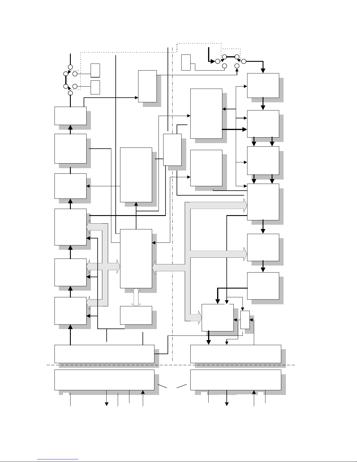
1.2 Modem Functional Assemblies
The PSM-500 VSAT/SCPC Modem consists of seven main functional elements arranged on three
electronic printed circuit assemblies, as shown in Figure 1-2.
The Main Modem Circuit Assembly consists of the following major assemblies:
1. The Modem digital PSK/QAM modulator with carrier generation in the 50 to 90 M Hz
range for standard modem, or 950 to 1750 MHz in the L-Band versions.
2. The Modem digital PSK/QAM demodulator accepting signals in the 50 to 90 MHz range
for the standard modem and 950 to 1900 MHz in the L-Band versions.
3. The Modem microprocessor monitor/control subsystem.
4. The Modem Digital Signal Processor Acquisition subsystem.
5. The Programmable Data Interface. Seven standard data interfaces are built onto the
main modem assembly. The unit can also accept special interfaces via an optional
interface card.
The other two printed circuit assemblies are the Front Panel Control Assembly, and the Power
Supply Assembly.
In addition the main PWB can accept two plug-in sub-assemblies for Forward Error Correction
(FEC). The first subassembly normally contains either the standard Viterbi and Reed-Solomon FEC
set or a combination card containing Viterbi/TCM, Reed-Solomon and either a 4k block size Turbo
Product Codes (TPC) or a 16k block size TPC. The TPC could also be installed alone on a card
placed in the second plug in location. The second location could also be one of a number of FECs
that are be available for the M500, such as FlexLDPC.
The IBS Multiplexer circuitry that was on another daughter card in previous modems is now part on
the main board’s FPGAs.
Note in the functional block diagram below that, with the exception of the receiv e FIFO buffer, there
are complementary signal processing blocks in the transmit and receive paths. Note also that there
are no typical superhetrodyne mixing and filtering blocks. That is because there are none used in the
direct modulation and demodulation scheme used in the PSM-500, sometimes referred to as Zero
IF.
The following sections described more detail on the design of the modulator and demodulator.
PSM-500/500L/500LT - Rev. 0.91
Page 17
PSM-500/500L/500LT SCPC Satellite Modem Description
Page 1-7
Doppler
FIFO Buffer
Program
mable
Transmit
Interface
DB37
Female
at J3
RS-449
or
V.35
or
RS-232
etc.
FEC
Encoder
Baseband Signal
Processing
Modulator
TClk
TData
RTS
CTS
V.35/Intelsat
and
Differential
Encoder
Programmabl
e Attenuator
Transmit SynthesizerProcessor Control
Option
Interface
Connector
P1
TT
Clk
Program
mable
Receive
Interface
DB37
Female
at J3
RS-449
or
V.35
or
RS-232
etc.
RClk
RData
Ready
Option
Interface
Connector
P1
Ext
FIFO
Clk
XMT Out
70 MHz
or L-Band
Figure - M500 Modem Block Diagram
FEC
Decoder
Baseband Signal
Processing
Demodulator
V.35/Intelsat
and
Differential
Decoder
Front end
AGC/Amp
A/D
Conversion
Receive Synthesizer
RCV In
70 MHz
(or L-Band)
Out Clk
In Clk
Modem
Reference
Oscillator
MODULATOR
DEMODULATOR
Interface & Loop-
Back Circuits
DSP Aquisition
Processor
25 dB
Loopback
Attenuator
Term
Term
Low
Pass
Filter
Term
Ext. Reference In
Clock
Control
Aux.
Con-
nection
at J4
PSM-500/500L/500LT - Rev. 0.91
Figure 1-2 Modem Block Diagram
Page 18

Description PSM-500/500L/500LT SCPC Satellite Modem
Page 1-8
1.2.1 Modulator
The PSK/QAM modulator in the modem employs a unique digital modulation scheme requiring no
heterodyne operations (mixing and filtering to an IF) to arrive at the transmit RF frequency. The
desired carrier frequency is synthesized and directly modulated with the baseband signal. The
baseband signal is itself digitally derived and generated using a digital to analog (D/A) convert er.
The digital signal processing of the transmit signal includes the equivalent of a 144 tap FIR filter
function.
As previously shown in Figure 1-2, synchronous transmit data and clock signals are accepted by the
modulator, then processed by the V.35/Intelsat scrambler and differential encoder. The m odulator
can be set by the processor to operate at a number of data rates between 1.2 kbps (BPSK, rate 1/2)
and 20 Mbps (8PSK +, M520 feature set). Refer to the specification in Appendix A for exact rate
capabilities. The data is then encoded for Forward Error Correction (FEC) at rate 1/2, 3/4, 5/6 or 7/8
resulting in an encoded signal at between 2.4 and 14,760 ksps (kilo symbols per second). The
Viterbi convolutional encoder can be programmed for rate 1/2, 3/4, 5/6 or 7/8 and is set for a
constraint factor (K) of 7 for use by a (receiving end) Viterbi convolutional decoder with the same
rate and K factor. A Reed-Solomon FEC is available for concatenated operation with the Vit erbi
Codec and two types of “Turbo Codes” Codecs are also available to replace the Viterbi Codec. A
special case is 8PSK, which only operates in a Trellis Code Modulation (TCM) mode at rate 2/3,
unless a non-Viterbi FEC is added such as TPC or FlexLDPC.
The FEC is followed by an optional differential encoder. The differential encoder out put is then sent
to the transmit baseband signal processor whose main function is to convert the data stream into
analog baseband I and Q channels for modulating the carrier. The actual conversion process is
accomplished in a lookup table, latch and D/A converter. The lookup table represents a digitally
preprocessed function required to produce the proper RF signal output when mixed with the desired
carrier frequency. A low-pass filter is applied to the D/A output to reduce the level of sampli ng
components.
Transmit Local Oscillator generation is accomplished in two parts. A PLL step synthesizer is used to
generate a basic LO in the 52 to 92 (or 104 to 184 or 952 to 1752) MHz range with 500 kHz step
size. A Direct Digital Synthesizer (DDS), consisting of an NCO and D/A conversion, is used to
generate an approximate 2 MHz signal with fine step size of approximately 1 Hz and a range of
±1.25 MHz. When the DDS is subtracted from the step synthesizer output in a second PLL, the
available LO can be tuned in 1 Hz steps over the full range of 50 to 90 MHz (100 to 180 MHz if built
for that version).
The processed baseband signal is then mixed with the transmit synthesizer's LO carrier signal to
generate an output modulated carrier in the 50 to 90 MHz range (or 950 to 1750 MHz in the L-Band
modem). A classic IQ modulator with two mixers is used and the LO is fed into the second mix er
shifted 90 degrees from the first. The modulated baseband signal can take two forms at this point
depending on whether BPSK or QPSK modulation is used. In BPSK mode, the baseband signal fed
to the two mixers is identical. In QPSK mode, the two signals represent the baseband I and Q
channels of the baseband.
The resultant RF signal is then low pass filtered and amplified to produce a signal at approximately
over 5 dBm into 75Ω. An output attenuator controlled by the onboard processor is used to set t he
modulator output level over a range of +5 to –35 dBm. The actual attenuator is a set of pin di odes
whose voltage is derived from the processor via a 12-bit D/A converter. The processor also holds a
calibration table of DAC input vs. RF output level/frequency in non-volatile memory.
No physical adjustments are present in the modulator. All necessary adjustments are electronically
performed during calibration and are intended to last the life of the unit without requiring resetting.
The modulator is capable of operating in two different modes: Continuous mode for SCPC use and
“Burst” mode for use at a VSAT location. When set to VSAT operating m ode, the transmit signal is
turned off and on according to the status of the data interface control lines and framing information in
the data stream as described in the “Operation” Chapter of this document. The burst mode allows
multiple station modulators to link up consecutively with a single master station “burst dem odul ator”.
PSM-500/500L/500LT - Rev. 0.91
Page 19

PSM-500/500L/500LT SCPC Satellite Modem Description
Page 1-9
Note: As of the time of this manual the burst mode is a special factory request option and not
installed in standard modems.
The Modulator IF output can be routed to the Demodulator input using a built-in “IF Loop-back”
function. The loop-back path provides a 25 dB attenuator to avoid overloading the receive input.
1.2.2 Demodulator
The Modem Demodulator uses direct conversion techniques for recovery of data from an incoming
carrier, and therefore like the modulator does not use heterodyning, and has no internal IF signal or
processing. Referring to Figure 1-2, the input RF signal is first input to the receive AGC amplifier.
The AGC amplifier has a range of greater than 40 dB at any data rate, allowing input s ov er that
range while still meeting performance criteria. The range is controlled in several steps depending on
the data rate extending over the range of –20 dBm at high data rates to –84 dBm at l ow dat a rat es.
The proper AGC gain is digitally determined as that which produces an optimal output from the A /D
converters and is thus derived after the A/D converters.
The RF input is then demodulated using a “Costas Loop”, phase locked loop demodulator where the
signal is split using a 90 degree hybrid into I and Q channels. In BPSK mode, the I channel carries
the data information and the Q channel represents the noise and carrier phase information in the
Costas loop. For QPSK operation, the I and Q channels each carry data information. The I and Q
channel “eye” signals are not available as in many other modems because the signal/data
representation at this point is still strictly digital for direct signal processing.
A receive synthesizer generates the demodulator local oscillator which is at the desired receive
carrier frequency. The synthesizer is tunable over the range of 50 to 90 MHz (or 950 to 1900 MHz in
the L-Band modems) and has two tuning components; the LO step synthesizer used to tune in steps
of 500 kHz, and a Direct Digital Synthesizer (DDS) component used to acquire and track the
received carrier. The DDS control has two tuning sources; (1) the digital Costas demodulation loop
phase detector used to track an already “locked” signal and (2) the processor control used to set the
carrier frequency and acquire new signals. The processor controls the acquisition search over a
programmable range from ±100 Hz to ±1.25 MHz.
The I and Q channel baseband outputs of the Costas Loop demodulator are converted to digital data
streams by parallel 12 bit D/A converters. The digital information is then filtered via a Datum
Systems’ proprietary programmable digital filter. The filtered sample output is sent to the input of the
Forward Error Correction (FEC) process (either Viterbi convolutional, concatenated Reed-Solomon,
8PSK TCM rate 2/3, Turbo Codes or LDPC decoder) circuit. Multiple bits of the filtered A/D
converter are used for “soft decision” decoding in the FEC, providing an improvement in
performance over hard decision decoding.
The A/D output is also available to a special Digital Signal Processor (DSP), which is used to
examine the incoming signals for known energy patterns and acquire carriers significantly faster
than conventional sweep acquisition. This DSP controlled acquisition is especially useful at low data
rates and can improve over a typical sweep by more than 2 orders of magnitude.
The receive signal processing shown in Figure 1-2 serves the following multiple functions:
1. Generates the soft decision symbol information for input to the FEC.
2. Recovers the bit rate clock from the incoming signal.
3. Measures the Es/No of the received signal.
4. Generates the receive AGC signal to set the input stage gain.
The FEC decoders are contained on one or two adaptor cards plugged into the main board (all
except the TPC are contained with the adaptors FPGA), which is under control of the onboard
processor.
A differential decoder and INTELSAT / V.35 descrambler for the received data signal can be
individually enabled or disabled by the processor based on the current FEC and other settings. It is
no longer under control of the front panel or command interface. This configuration is held in the
PSM-500/500L/500LT - Rev. 0.91
Page 20

Description PSM-500/500L/500LT SCPC Satellite Modem
Page 1-10
nonvolatile EEPROM and does not have to be reconfigured on power-up. The resulting received
data and clock signals are sent to the interface assembly. Receive interface clocking can take
several forms as explained below.
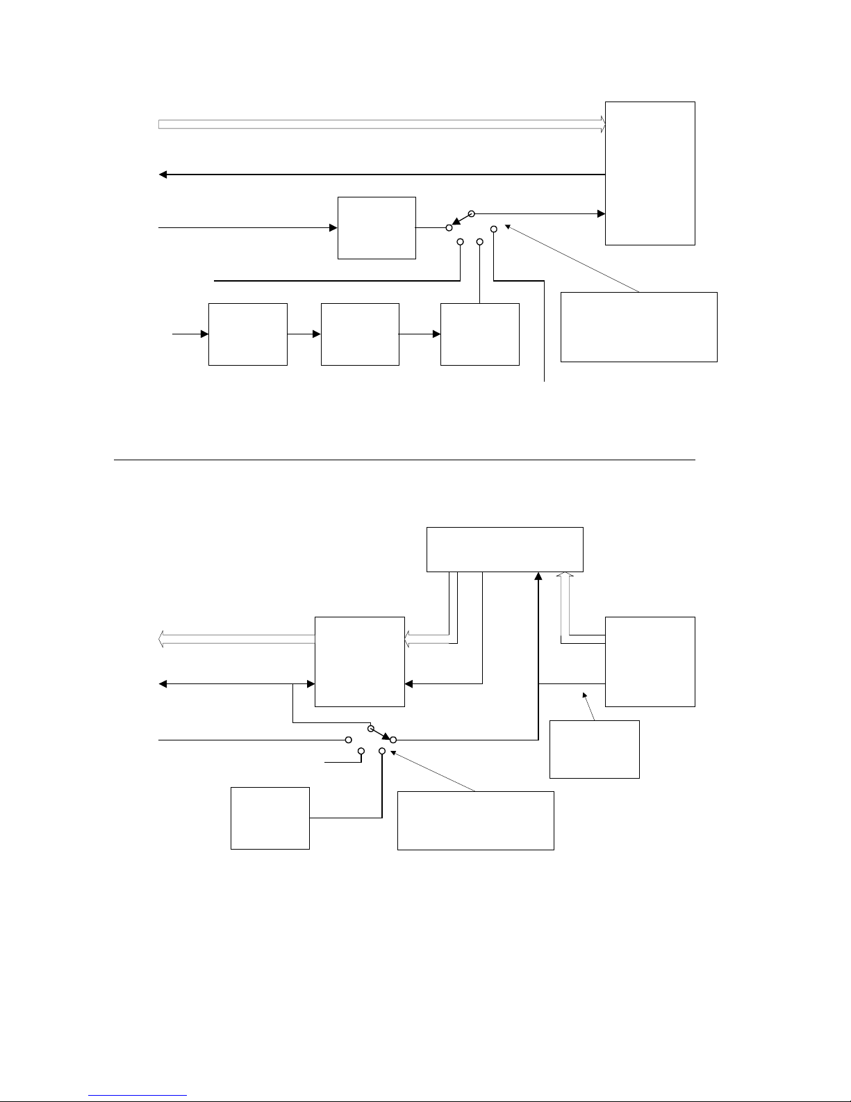
1.2.3 Modem Bit Rate Timing
The Modulator and the Demodulator each have 4 possible sources for their bit rate timing.
The Modulator always outputs the Send Timing signal, but the source of this tim i ng m ay be either:
1. An Internally generated bit rate NCO locked to the Internal Reference,
2. The Demodulator Receive Clock,
3. An External input at the data rate or
4. An external input on the Interface Terminal Timing input.
The modem’s internal reference is a 2.0 parts per million clock oscillator, which is sufficiently
accurate for most applications. If system timing requirements dictate a better reference, the i nternal
oscillator may be phase locked to an external reference applied at the rear panel.
The Demodulator always outputs the Receive Timing signal. The receive demodulator clock derived
from the receive signal is synchronous with the Receive Data and is the normal source of the
receive timing. If the system requires a different clock (which still must be the same av erage rate as
the demodulator’s receive clock) then provisions are made to buffer the data in a programmable
FIFO. The demodulator receive clock is always used to clock the data into the FIFO. The clock
output can be either:
1. The Demodulator Receive Clock,
2. The Modulator Clock
3. An internally generated bit rate NCO locked to the Internal Reference, or
4. An External FIFO Clock applied on the interface connector.
If the demodulator receive clock is selected then the FIFO itself is physically bypassed by switching
circuitry.
The internally generated bit rate NCO locked to the Internal Reference oscillator is settable to 40 bi t
accuracy. That is 1 part in 10 to the 12 or 1 part per trillion.
The PSM-500 series includes two changes to previous modems to insure proper operation. First, the
modem detects if no data is present on the input by a lack of transitions for approximately 5 seconds
and will produce a programmable alarm after that time. Second, due to the higher data rat es the
PSM-500 input circuitry automatically fine tunes the clocks to attempt to place the data period at the
optimal point with respect to the clocks. This also helps tremendously when using the TT clock to
create the transmit timing.
A block diagram simplified representation of the Transmit and Receive clock sources are shown in
Figure 1-3.
PSM-500/500L/500LT - Rev. 0.91
Page 21
Page 1-11
Transmit Clock Sources
Receive Clock Sources
Demodulator
Modulator
Receive FIFO
Buffer
DATA
CLOCK
DATA
IN
INOUT
OUT
DATA
Optional Reed-Solomon Decoder
& IBS Multiplexer
CLOCK
Demodulator RCV
External
Reference Input
(Rear Panel)
From Modulator
bit timing
CLOCK
Internal
Reference
Oscillator
External
Reference PLL
Terminal
Timing
Terminal
Timing
From
Interface
Demod output
clock is phase
locked to receive
bit timing
FIFO output clock selected from
"RCV Clock", "Internal", "External"
or "Mod Clock". Selection of "RCV
Clock" bypasses the FIFO buffer.
Bit Rate NCO
From
Receive
Clock
Send Data
From
Interface
Send
Timing To
Interface
Modulator bit clock source is
selected from "Internal", "Terminal
Timing", "External" or "RCV
Clock". The Send Timing is
always an output from the modem.
Receive
Data To
Interface
Receive
Timing To
Interface
External
FIFO Clock
From
Interface
Bit Rate NCO
"Internal"
External Send Timing Input
(Rear Panel)
PSM-500/500L/500LT SCPC Satellite Modem Description
These Clock sources may be used in various ways in a system implementation to provide correct
timing at a destination. Each of the clock sources can be set either from the front panel or from an
external monitor and control system.
PSM-500/500L/500LT - Rev. 0.91
Figure 1-3 Clock Source Options
Page 22

Description PSM-500/500L/500LT SCPC Satellite Modem
Page 1-12
1.2.4 Control Processor
A single microprocessor manages all monitor, control and communications functions on the modem
board. The processor continuously monitors all onboard status signals.
The modem control processor uses external address and data buses to connect to external Flash
PROM containing the instruction code. The processor uses both internal and external RAM for all
operations and maintains configuration and permanent parameters in parallel EEPROM. The
processor also connects to the FEC, the custom ASICs, the DSP processor, the front panel, and
various onboard peripheral functions via the address and data bus.
The control processor also maintains a serial peripheral interface to connect to several onboard
peripherals. These include external D/A converters holding calibration and current analog settings,
identification EEPROMs on option and interface cards and step synthesizers.
The control processor also contains an internal 12-Channel 10-bit A/D converter for gathering
analog information from various onboard monitored points including the phase locked loop tuning
voltages.
Digital I/O used to monitor and control the modem is handled mainly through the DSP circuits and
their interface to the processor. Such parameters as the current Eb/No and receive offset frequency
information are read by the processor from the DSPs while most configuration information is writt en
to the DSPs.
The control processor uses a full-duplex Universal Asynchronous Receiver/Transmitter (UART) for
communications with either the RS–232 / RS–485 remote command port or with a separate VT100
type “console” terminal device connected to the modem. In addition a USB control int erf ace i s
provided.
The control processor has provisions for communicating with another PSM-500 modem for
implementation of Automatic Uplink Power Control (AUPC). The channel for this communications is
normally provided by equipping the unit with the optional IBS multiplexer interface card.
1.2.5 Acquisition Processor
The acquisition processor, a Texas Instruments 320C5xxx Digital Signal Processor, manages the
receive signal acquisition and lock functions to achieve fast acquisition performance at low data
rates. This DSP is controlled by the control processor via a communications protocol managed
through a special bi-directional parallel interface to the main processor.
The signal acquisition DSP accepts sampled data from the receive chain A/D Converters and
mathematically determines the location of the incoming carrier. This is accomplished in a multi–step
process which continues to narrow down the exact frequency until it is known within the lock range
of the PLL demodulator. At data rates below 16 kbps this process is more than an order of
magnitude faster than a standard sweep method. Typical signal acquisition times at 16 kbps QPSK
are 0.2 seconds using the acquisition processor vs. over 20 seconds using a standard sweep.
1.2.6 Standard Data Interface
The standard Interface in the PSM-500 is built onto the main PWB and contains the driv ers and
receivers for one of five possible data interface standards (seven including minor variations of each).
All interface standards are selected under program control via the front panel or remote control. Five
of these standards are common interfaces used in the communications industry:
• RS-449, terminated and un-terminated
• V.35,
• V.36
• Synchronous RS-232 (Limited to 128 kbps by drivers and receivers.)
• EIA-530 and EIA-530A
• Asynchronous RS-232 (Limited to 115 kbps by various protocols).
PSM-500/500L/500LT - Rev. 0.91
Page 23

PSM-500/500L/500LT SCPC Satellite Modem Description
Page 1-13
The un-terminated versions of these standard interfaces and are used to implement one for one
(1:1) redundancy between two PSM-500 units.
A single 37 pin “D” type female connector is available on the rear panel at J3 providing the terrestrial
data interface. The interface standard is electronically selectable via front panel or remote control.
Optional interfaces are provided by a separate option interface card which is mounted inside the
modem chassis. The provision of an optional interface “adds” to the available interfaces which can
be selected under program control. An interface field kit of parts to add an option interface is
available from the manufacturer for installation by qualified technical f i eld servi ce personnel. When
an optional interface is installed the main processor automatically queries and installs the necessary
software controls for accessing the interface.
1.2.6.1 Data Interface Loop-Back Function
The standard and most optional interfaces also provide the data loop-back function. Ethernet
interfaces do not have this function. The data loop-back can be controlled from the front panel or via
remote control command. The data towards both the terrestrial and satellite sides can be looped
back individually by enabling this function via the front panel or remote control
⇒
Caution: Enabling the “Data Loop-Back” functions will result in loss of traffic. It
should not be used in operating links without prior arrangements.
The data loop-back allows testing of the signal path connection up to the loop-back and back to the
source. Since both terrestrial and satellite sides of the signal path can be looped, the connection
from a local DTE can be checked on the terrestrial side while the connection from the far end DTE
over the satellite and through the modem can be checked on the satellite side.
More information on use of the loop-back modes is given in Section 4.1 Common Test Procedures.
1.2.6.2 Data Interface BERT Function
The standard interfaces also include a programmable Bit Error Rate Test (BERT) set. It is located
between the modem’s satellite and terrestrial data loop-back functions. Ethernet interfaces do not
have this function. The BERT can be controlled from the front panel or via remot e cont rol comm and
and provides extensive test result data.
⇒
Caution: Enabling the “BERT” function will result in loss of traffic. It should not be
used in operating links without prior arrangements.
New in this modem is the ability to set the BERT set to point toward t he “Li ne” side external cabling,
acting as a DCE device. More on use of the BERT functions and modes is given in Section 4.1.2
“Using the Built-in BERT”.
1.2.6.3 Data Interface 1:1 Redundancy Function
The standard interfaces are also capable of operating in a special 1:1 redundancy mode. In this
mode the data interfaces are tied directly in parallel using a special “Y” cable. Software control built
into the modem can then be set to indicate that the two connected modems are operating in a
redundant mode. The two modems communicate with each other to determine the alarm status of
each and force the “off-line” unit’s data interface into an un-terminated condition. This allows both
interfaces to receive incoming data and clock signals, which are necessary to ascertain correct
functioning. At the same time the transmit and receive IF ports are also connected together through
the stations (or separately supplied) transmit and receive IF combiner/splitter assemblies.
The alarms that are used to determine switching criteria are programmable, and the first modem set
up for this mode automatically loads its configuration information to the second or “back-up” unit.
These features create a very low cost redundancy system that is both flexible and easily set up.
More information on the set-up and use of the 1:1 redundancy functions and modes is given in
Sections 2.3.5 “1:1 Redundancy Connection” and 3.10 “Built-in 1:1 Redundancy Mode Operation”.
PSM-500/500L/500LT - Rev. 0.91
Page 24

Description PSM-500/500L/500LT SCPC Satellite Modem
Page 1-14
Compatibility
Ratio
Disabled
N/A
1/1 Standard
IESS-309
16/15
Fixed synchronous ESC, No AUPC, No MCC
MCC).
Also variable data load per frame.
1.2.7 Standard Framing and IBS Multiplexer
The framing/multiplexer is capable of multiplexing a relatively low speed overhead channel onto the
terrestrial data stream resulting in a slightly higher combined or “aggregate” data rate through the
modem. The overhead channel is recovered at the far end. This added channel is termed variously
an overhead channel, ESC, service channel, “asynch” channel or, in IESS terminology, an E S to ES
data channel. A simplified block diagram of the data multiplexer is shown in Appendix RS .
The basic frame structure used by the multiplexer is that specified in the IESS-309 standard, P age
60, Figure 10, resulting in a 16/15 aggregate to through data ratio. This means that when the
multiplexer is enabled the modem aggregate operating data rate is computed as the terrestrial
connection (through) data rate multiplied by 16/15. The user sets only the desired through data rate
while the modem computes the aggregate rate required. The multiplexer is also capable of
expanded operating modes which include custom setting of the ratio of data to framing by tes.
The Multiplexer provides the following modes of operation. They are described more fully i n T he IBS
Multiplexer/Reed-Solomon Appendix RS.
Mode Standard/
Overhead
Notes
Enhanced Modified IESS-309 16/15 M4 compatible ESC and AUPC (limited
Custom Modified IESS-309 Variable Full ESC and MCC including AUPC, Remote
Modem Control, 2 one=bit control channels.
The ESC Data Channel can be set under software-control to either RS-232 or RS-485 mode. The
pin assignments for both modes are shown in Section 2.3 and Appendix RS. These pin assignments
appear on the rear panel “AUX” (Auxiliary) connector J4 only when the Multiplexer function is
enabled. The RS-485 Transmit Data Drivers can set to “RS-485” or “RS-485 ON” when in
“Enhanced” mode. The “ON” setting forces the driver continuously on while the “RS-485” setting
controls the output into tri-state when the modem is not transmitting data, al lowing m ul tiple modem
outputs to be connected together. In the standard IBS mode only the “RS-485 ON” mode is
available.
In Enhanced or Custom mode a 2 wire receive operating mode can be selected for the receive data
into the ESC channel. In this mode the receive input is muted while the transmit data output is
active. In 4 wire mode the receive is always enabled. In the standard IBS mode only the 4 wire mode
is available. Note that the transmit and receive pairs are physically separate wires and must be
connected together if true RS-485 2 wire connectivity is desired.
The processor on the main board performs software/hardware assignment of bits to specific
purposes in the Custom mode and buffers the ESC Data Channel to standard asynchronous data
rates.
The user does not have to compute data framing variables to use the Custom Multiplexer Mode.
When placed in this mode the entry parameters are the ESC and MCC channel rates selected from
standard asynchronous data rates (300 to 38,400 bps). The modem then computes the proper
relationship between the framing and terrestrial data rates to achieve the proper operation. The
modem also displays the terrestrial data to aggregate ratio.
PSM-500/500L/500LT - Rev. 0.91
Page 25

PSM-500/500L/500LT SCPC Satellite Modem Description
Page 1-15
1.2.7.1 Modem Control Channel (MCC)
The MCC is available in both the Enhanced and Custom Multiplexer modes. In the Enhanced mode
the MCC provides for an AUPC channel. In the Custom mode the MCC provides for the AUPC plus
the Remote Modem Control (RMC) Channel and the Auxiliary control bits (RFC).
1.2.7.1.1 AUPC Control Channel (AUPC)
When the modem is placed into either the “Enhanced” or “Custom” modes the AUPC control
channel becomes available. The AUPC operation itself is under control of the modem while the
AUPC facility in the MCC provides the channel for the information. Thi s channel prov i des a m i ni m um
300 baud control channel in each direction to allow the modems at two ends of a link to interactively
maintain the receive Eb/No by controlling the power output at the transmit site.
Refer also to the AUPC operation description of the main manual in Section 3.8 titled “Automatic
Uplink Power Control (AUPC)” Operation.
1.2.7.1.2 Remote Modem Control Channel (RMC)
When the modem is placed in the “Custom” mode the Remote Modem Control Channel becomes
available. This channel allows the control of a far end modem from the near end site. This cont rol i s
not however allowed from the near end front panel, but only via the remote control interface port.
The command protocol for remote unit control is explained in Appendix B, “Remote Control
Protocol”.
Note that the Automatic Configuration Recovery or ACR is partially designed as a safet y feature to
be used with the remote programming of modems. It can help prevent “losing” the modem at an
unattended site. Refer to the ACR section of the main manual in 3.14 “Automatic Configuration
Recovery”.
1.2.7.1.3 Auxiliary Bit Control Channels (RFC)
When the Multiplexer is placed into the “Custom” mode the auxiliary bit control RFC channels
becomes available. These consist of two single line or “one-bit” control channels that can be used to
send control information independently in both directions over the link. The input signals on t hese
channels can be either a contact closure or a logic type signals while the output is a form C relay
contract set whose state depends on the state of the input signal. The low input logic level is 0 to 0.4
VDC, while the logic high level can be from 2.4 to approximately 20 VDC. The input is current limited
to accept this wide voltage range without damage. Higher voltages may damage the input s howev er
and caution should be exercised. Pin connections for these one bit channels are shown in the RS
Appendix.
1.2.8 Standard and Optional Modem FEC Cards
All of the M500 class modems have two card slots on the main PCB for two FEC function boards.
One board is normally installed containing the standard Forward Error Correction set including
Viterbi (with Trellis Code Modulation mode when in 8PSK mode only) and Reed-Solomon
concatenated codecs. The same standard card has several variations which includes either a 4k or
16k block size TPC or both on the same board if ordered that way initially. The second slot can be
used for optional FECs as desired, for example the FlexLDPC FEC featuring exceptional
performance at very low Eb/No.
These two FEC slots are wired in parallel and the control processor on the main board searches for
a requested FEC on the first card containing that capability. The same FEC functions can exist on
both cards, but only the first card will be used in that case.
FEC technology is in many ways a matter of tradeoffs. In most cases the t radeof f is between
bandwidth and performance, which also relates to power and performance. FECs are normally
specified by “Rate”, which is the ratio of data information bits to transmitt ed bits, and coding gain,
which is the Eb/No reduction able to achieve a specified BER as compared to an unencoded signal.
The extra bits required for a given rate are redundancy processing bits needed to perform forward
PSM-500/500L/500LT - Rev. 0.91
Page 26

Description PSM-500/500L/500LT SCPC Satellite Modem
Page 1-16
error correction. For example, the common rate ½ means that for every data bit two bits are
transmitted, and in rate 5/6, 6 bits are transmitted for every 5 dat a bi ts. Better performance is
commonly considered higher coding gain at a given rate. There are always other factors to consider,
such as the latency (processing time) required, time to recover from a synch loss, signal acquisition
time, etc, etc.
FECs technology is often specifically adapted to a particular use. For example, it is comm on to use
special forms of Reed-Solomon, TPC and LDPC for video signals. These type signals and FECs
typically have a fairly high performance floor that are of litt l e consequence for a wideband video
signal, but would be entirely unacceptable for most data information especially at low data rates.
Viterbi has been the standard high performance FEC used in satellite communications for
approximately 10 years. It has only been in the past few years that new t echnologi es hav e em erged
which provide more coding gain with reasonable implementations. The standard PSM-500 FEC card
includes the circuitry for a Viterbi, TCM and Reed-Solomon Codec providing the PSM-500 with basic
functional capability for all standard operating parameters including 8PSK TCM and 16QAM. T he
following are general descriptions of the characteristics of each of these functions.
The table below shows the currently available modes depending on modulation.
Note in Table A that the front panel selection number for each of the options is list ed as t he “S el #”.
For example The Modulation modes show the selection numbers 0 through 6, and the FEC Type,
Option and Code Rate selection numbers are listed in the column to the right of each item. These
numbers can be referred to for front panel operation but are even more applicable to the SnIP Telnet
command line program named “m500ctl”. This program has specific commands that allow entering
either just the 3 digit FEC options or the full M
odulation, FEC Type, Option, Code rate and Reed-
Solomon mode (MTOCR) in a single entry. Refer to the SnIP documentation for more information.
PSM-500/500L/500LT - Rev. 0.91
Page 27
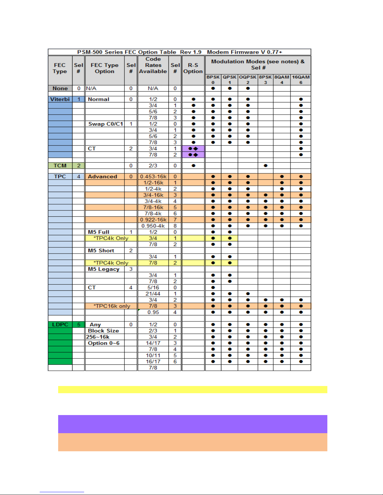
PSM-500/500L/500LT SCPC Satellite Modem Description
Page 1-17
1. The TPC M5 Full, Short and Legacy modes are intended for PSM-4900 Compatibility only
2. * TPC 4k/16k restrictions apply to that line and Code Rate only
3. TPC4k Max data rate limits see below
4. TPC16k operates up to 20 Mbps depending on Feature Set and modulation
5. The Viterbi, Rate 3/4 & 7/8, 16QAM CT modes are only for Comtech modem compatibility as
they only operate in this mode with R-S at 220, 200, depth of 4. R-S is auto-enabled
6. TPC Advanced modes are Datum Systems proprietary implementations that require the
TPC16k option only for the colored lines. They offer superior performance to CT modes
PSM-500/500L/500LT - Rev. 0.91
Page 28

Description PSM-500/500L/500LT SCPC Satellite Modem
Page 1-18
1.2.8.0 Special Codec CT Modes
The wide range of FECs available today and the possibility of many diff erent operating modes and
parameters for each can make compatibility with other brands of modems extremely difficult. To ai d
in FEC compatibility with other brands of modems, the PSM-500 series offers special “CT” modes,
standing for “Competing Technology”. These modes use the same parameter settings as popular
modems by other manufacturers.
Take note of the special CT modes available for Viterbi, Reed-Solomon and TPC modes below.
1.2.8.1 Viterbi, Trellis Code Modulation Codec
Viterbi has been the standard high performance FEC used in satellite communications for
approximately 10 years. It has only been in the past few years that new technologies have emerged
which provide more coding gain with reasonable implementations. Viterbi still maintains the
advantage of fairly high coding gain with very low latency. So, for voice circuits or DAMA links
requiring fast acquisition times Viterbi may be the FEC of choice.
Viterbi is part of a class of FECs considered “convolutional”, basically meaning folded as in the
redundancy bits are folded into the data bit stream. The important issue here is that it is not block
oriented and not framed. It is therefore the responsibility of the FEC decoder to determine which are
the proper data bits.
Trellis Code Modulation or “TCM” is a standard part of the M500 used with 8PSK at rate 2/3.
The Viterbi CT option mode follows that of competitive modems for 16QAM operation at rates ¾ and
7/8. The CT mode at this setting defaults to selecting Reed-Solomon CT mode at n, k and depth
values of 220, 200, depth of 4 and inverts the data. This is a closed circuit mode that does not meet
normal IESS standards, but is necessary in order to link to those modems.
1.2.8.2 Reed-Solomon Codec Capability
Reed-Solomon Codec places a second Forward Error Correction (FEC) process outside of and in
series with the existing Viterbi FEC. The two FECs are thus considered "Concatenated". In addit i on,
the data between the two FECs is "interleaved" which effectively reduces the possibility of multiple
consecutive errored block symbols, thus improving the Reed-Solomon Codec performance.
The performance improvement achieved by this combination is significant. For example, the BER vs.
Eb/No performance of concatenated Viterbi rate 3/4 coding with R-S is better than Viterbi rate 1/2
alone and it uses less bandwidth than the Viterbi rate 1/2 alone.
Reed-Solomon is a block oriented code, meaning that data is framed into fixed size blocks and
processed in a specific way. A full block must be received before processing can begin, thus adding
to the latency. The PSM-500 type R-S Codec is capable of operating in multiple standard and
custom modes as shown in the table below.
Reed-Solomon uses framing which allows the use of a synchronous scrambler resulting in slightly
improved performance relative to the self-Synchronized scrambler normally used.
A simplified block diagram of the Reed-Solomon Codec is shown in the Figure below.
PSM-500/500L/500LT - Rev. 0.91
Page 29
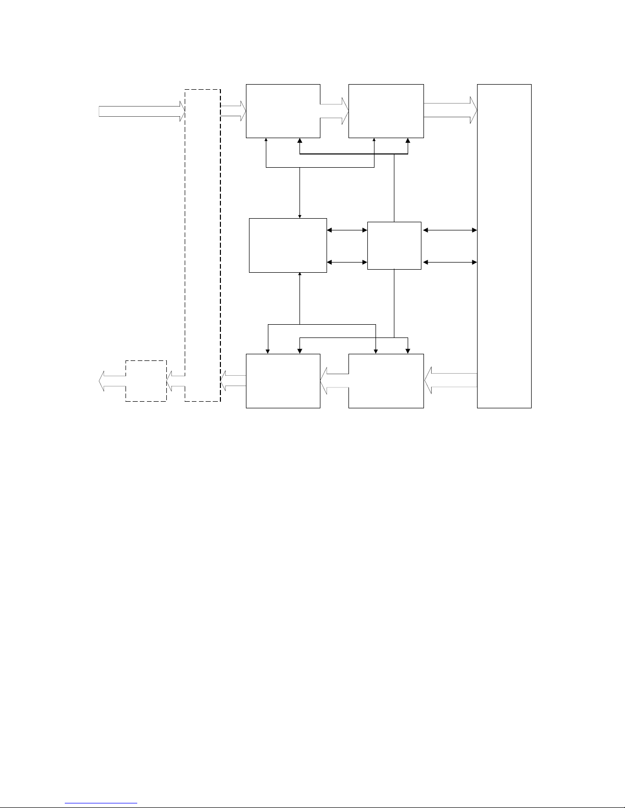
PSM-500/500L/500LT SCPC Satellite Modem Description
Page 1-19
Transmit Reed-Solomon
Block Encoder &
Synchronous Scrambler
Processor
Transmit
Terrestrial Data
Channel
Receive
Terrestrial Data
Channel
Transmit
Data Channel
Receive Data
Channel
Control
XMT
Clock and Frame
Generation
RCV
Control
Clock
Clock
Main Modem
Assembly
Clocks
Reed-Solomon Codec Simplified Block Diagram
Transmit Reed-Solomon
Block Interleaver
Receive Reed-Solomon
Block Decoder &
Synchronous
Descrambler
Receive Reed-Solomon
Block De-Interleaver
FIFO From
Main Modem
IBS
Multiplex
Option
The Reed-Solomon modes shown available below can be selected from the front panel or remote
control. The CT220,200 mode is a special compatibility mode and is automatically set by cert ai n CT
FEC modes, for example when Viterbi, Rate ¾ is selected when in 16QAM mode. It can be overridden by choice from the Reed-Solomon parameter.
PSM-500/500L/500LT - Rev. 0.91
Page 30

Description PSM-500/500L/500LT SCPC Satellite Modem
Page 1-20
Data Rate
Ratio
Disabled
N/A 1/1
<1.544 Mbps
<2.048 Mbps
IESS-308
>2.048 Mbps
73/67
219, 201, 4
IESS-309
IESS-309
All
73/67
219, 201, 4
CT220,200
Comtech
All
11/10
220, 200, 4
max M4 data rate.
Mode
IESS-308 IESS-308 1.2 kbps to
IESS-308 1.544 Mbps to
Custom Modified
Compatibility
IESS-309
Terrestrial
Overhead
n, k and depth Values
9/8 126, 112, 4 (M4 modem compatible)
45/41 225, 205, 4
All Variable Allows setting the “n”, “k” and “depth”
values for special requirements. Can
also be set for M4 compatibility to
The IESS 308 mode automatically adjusts the n and k factors dependent on the data rate. T he
“Overhead” ratio is the ratio of the data rate at the R-S encoder output to the data rate at the input. It
is defined as n/k. The modem automatically adjusts to accommodate the new rate.
The Reed-Solomon Codec function can be turned on and off under software control, and is
independent of the IBS ESC Data Channel enabling.
1.2.8.3 Turbo Product Codes FEC Capability
The addition of the Turbo Product Codes (TPC) option allows replacement of the standard Viterbi
FEC selectively for the transmit and receive paths independently. The performance improvem ent
achieved by the TPC is significant. For example, the BER vs. E b/No performance of TPC Rate ¾ is
approximately equal to Rate ½ Viterbi and uses over 40% less bandwidth. TPC also provides bet ter
bandwidth/power utilization than either Reed-Solomon concatenated on Viterbi or 8PSK/TCM with
Reed-Solomon.
The PSM-500 series offers extensive TPC capabilities including both first generation 4k block TPC
with both PSM-4900 compatibility (M5) and Competitive Technology (CT) operating modes plus a
newer second generation 16k block TPC. This second TPC offers superior performance at the
expense of more delay due to larger processing blocks.
The Datum Systems’ proprietary TPC “Advanced” mode has been optimized to provide the highest
performance available in any TPC on the market. These modes not only outperform other
manufacturer’s TPC, but also LDPC in many cases.
The Turbo Product Codes FEC is more fully explained in Appendix TPC.
1.2.8.4 FlexLDPC FEC Capability
The addition of the FlexLDPC FEC option allows replacement of the standard Viterbi FEC selectively
for the transmit and receive paths. The performance improvement achieved by FlexLDPC is the
highest and most flexible of any specialized FEC technology to date, outperformi ng TPC in across
all modes. FlexLDPC at rate ½ are capable of operating at a sustained Eb/No of only 1.5 dB with an
error rate less than 10
-9
.
PSM-500/500L/500LT - Rev. 0.91
Page 31

PSM-500/500L/500LT SCPC Satellite Modem Description
Page 1-21
1.2.9 Optional Interface Capability
The M500 modems are also capable of accepting optional interface cards to replace the standard
synchronous serial interfaces. The first of these cards is the Ethernet interface embodied in the
Datum Systems’ Satellite Network Interface Processor, or “SnIP”. The SnIP is m ore fully explained
in Appendix SNIP.
A second specialized interface card available is a High Speed Serial Interface or HSSI that is
commonly used for connection to some routers. The HSSI interface is more fully explained i n
Appendix HSSI.
For users that require the option to select either SnIP or HSSI interfaces in addition to the standard
synchronous serial interfaces, both cards can be installed in a “stacked configuration.
Installed option interfaces are automatically recognized by the modem, making them a selectabl e
option on the front panel or remote control protocols.
1.2.10 Modem Circuit Implementation
Much of the functionality in this modem has been achieved by incorporation of ext ensive circuitry
into Digital Signal Processing parts and Field Programmable Gate Arrays (FPGA). Depending on
features and options installed there are between 1.2 and over 2 Million gates of logic encapsulated
in the FPGAs, a 10 fold increase over the last generation modem. The logic can be augmented and
changed as requirements change. The modems unique direct modulation and demodulation scheme
also completely eliminates all IF mixing and filtering circuitry.
PSM-500/500L/500LT - Rev. 0.91
Page 32

Page 33

PSM-500/500L/500LT SCPC Satellite Modem Installation
Chapter 2 - Installation
2.0 Installation Requirements
The PSM-500 VSAT/SCPC Modem is designed for installation in any standard 19-inch
equipment cabinet or rack, and requires 1 RU mounting space (1.75 inches) vertically and 12
inches of depth. Including cabling, a minimum of 15-inches of rack depth is required. The rear
panel of the PSM-500 is designed to have power enter from the left and IF cabling enter from the
right when viewed from the rear. Data and control cabling can enter from either side although
they are closer to the left. The unit may be placed on a table or suitable surface as required.
⇒
CAUTION: There are no user-serviceable parts or configuration settings located
inside the PSM-500 modem case. There is a shock hazard internally at the power supply
module. DO NOT open the modem case unless power is removed for option installation.
⇒
CAUTION: Before initially applying power to the modem, it is a good idea t o
disconnect the transmit output from the operating satellite ground st ation equipment. This
is especially true if the current modem configuration settings are unknown, where
incorrect setting could disrupt existing communications traffic.
2.1 Unpacking
The PSM-500 Modem was carefully packed to avoid damage and should arrive complete with the
following items for proper installation:
1. PSM-500 Modem Unit. L-Band Units may include an external BUC power supply.
2. Power Cord, 6 foot with applicable AC connector.
3. Installation and Operation Manual plus other information on CD.
2.1.1 Removal and Assembly
If using a knife or cutting blade to open the carton, exercise caution to ensure that the bl ade does
not extend into the carton, but only cuts the tape holding the carton closed. Caref ull y unpack the
unit and ensure that all of the above items are in the carton. If t he Prime AC power available at
the installation site requires a different power cord/AC connector, then arrangements to receive
the proper device will be necessary before proceeding with the installation.
The PSM-500 Modem unit is shipped fully assembled and does not require removal of the covers
for any purpose in normal installation. All normal hardware configuration, including setting the
data interface type and IF impedance is under software control. The type of Feat ure Sets, FEC
Options and Interface Options installed can be read from the LCD display on the front panel
under <Unit: Status – > column by scrolling down after initial application of power.
Should the power cable AC connector be of the wrong type for the installation, either the cable or
the power connector end should be replaced. The power supply itself is designed for world-wide
application using from 90 to 264 VAC (100 to 240 VAC +/- 10%).
2.2 Mounting Considerations
When mounted in an equipment rack, adequate ventilation must be provided. The ambient
temperature in the rack should preferably be between 10 and 35° C, and held constant for best
equipment operation. The air available to the rack should be clean and relatively dry. The m odem
units may be stacked one on top of the other to a maximum of 10 consecutive unit s before
PSM-500/500L/500LT - Rev. 0.91 Page 2-1
Page 34

Installation PSM-500/500L/500LT SCPC Satellite Modem
providing a 1 RU space for airflow. Modem units should not be placed immediately above a high
heat or EMF generator to ensure the output signal integrity and proper receive operation.
Do not mount the PSM-500 in an unprotected outdoor location where there is direct contact with
rain, snow, wind or sun. The modem is designed for indoor applications only.
The only tools required for rack mounting the PSM-500 is a set of four rack mounting screws and
an appropriate screwdriver. Rack mount brackets are an integral part of the front panel plate of
the unit and are not removable.
The following interface connections should be available at the mounting location as a minimum:
1. Prime AC power.
2. A 75Ω Transmit IF cable with BNC male connector. (50Ω optional) or a 50Ω Transmit
IF cable with type N male connector for the L-Band version.
3. A 75Ω Receive IF cable with BNC male connector. (50Ω optional)
or a 75Ω Receive IF cable with type F male connector for the L-Band versions.
4. A Terrestrial data interface cable to mate with the modem or installed option; ei ther a
37-pin male “D” sub connector for all standard or appropriate connector for an
optional interface (such as G.703 or Ethernet 10 Base T).
Other optional connections are shown below.
2.3 Modem Connections
All modem connections are made to labeled connectors located on the rear of the unit: The
connector definitions below are those on the modem unit. Any connection interfacing to the
modem must be the appropriate mating connector. Cabling and Connections are detailed in
Appendix C, “Cabling Specifications”. Refer to Figure 2-1 to locate the following connectors:
Prime AC power to the far left IEC male input at J1:
90 to 260 VAC, 47 – 63 Hz.
Maximum unit power consumption is 50 Watts (Typical < 30 Watts).
Integral switch provided as part of power entry connector.
Chassis ground connection at #8 stud location J2.
Data Interface Connection at Data Connector J3:
Standard RS–449 Connector (37-pin female “D” sub connector).
DB25 adaptor cable supplied with modem for V.35, E IA 530, RS-232.
Alarm Connection at 9-pin male “D” connector J5.
RS–485 Control Port connection at 9-pin female “D” sub connector J6:
Shield ground on pin 15
Transmit A on pin 6 (output from modem)
Transmit B on pin 1. (output from modem)
Receive A on pin 9 (input to modem)
Receive B on pin 8. (input to modem)
OR
RS–232 Control port connection at 9-pin female “D” sub connector J6:
Transmit on pin 3 (input to modem)
Receive on pin 2 (output from modem)
Common on pin 5.
Page 2-2 PSM-500/500L/500L T- Rev. 0.91
Page 35

PSM-500/500L/500LT SCPC Satellite Modem Installation
The Modulator 70 MHz IF Output at female BNC J7
50 – 90 MHz
Programmable +5 to –35 dBm output at 75Ω
Programmable +3 to –35 dBm output at 50Ω.
The L-Band Modulator (PSM-500L) L-Band IF Output at female Type N J7
950 – 1750 MHz
Programmable +3 to –35 dBm output at 50Ω.
BUC Power Source (normally 24VDC @ <4A) to be output on this connector. Various
supplies are available and all are connected to the 5 pin DIN connector at J10.
Programmable 10 MHz Reference signal to be output on this connector.
⇒
CAUTION!: Extreme Care should be exercised when connecting test
equipment in the transmit line either directly to the modem output or within the
line to the BUC. The voltage present to power the BUC can cause severe
to the input of test equipment like spectrum analyzers. A DC Block device is
highly recommended for test equipment connection.
⇒
CAUTION!: Extreme Care should be exercised when handling the transmit
cable as it is possible to have hazardous voltages on the transmit line. When
higher voltages are used to supply BUCs that require 48VDC the transmit line
can seriously
injure personnel.
damage
To avoid injury or equipment damage unplug the L-Band modem
and BUC power supply whenever the transmit cable is
disconnected!
The L-Band Modulator (PSM-500L) Block Up Converter Power Supply at J10
12 to 56 Volts DC, up to 6 Amp capability .
Programmable enable and disable onto the transmit cable at J7
The BUC Power Status LED next to J7 shows the status as follows
Red – No voltage sensed on DIN input connector or power is input and the
enabled but the cable to the BUC is shorted.
Green – Power sensed and enabled (connected) to transmit cable
Off – Power sensed but disabled (disconnected) from transmit cable.
The Demodulator 70 MHz IF Input at female BNC J9, 50 – 90 MHz
–20 to –60 dBm input at 75 or 50Ω. (to –84 dBm at lower bit rates)
The L-Band Demodulator (/L) L-Band IF Input at female Type F J9
950 – 1900 MHz
–20 to –60 dBm input at 75Ω. (to –100 dBm at lower bit rates)
Programmable 0, 13VDC or 18VDC @ <500mA to be output on this connector
Programmable 10 MHz Reference signal to be output on this connector.
⇒
CAUTION: Extreme Care should be exercised when connecting test
equipment in the receive line to the LNB. The voltage present to power the LNB
can cause severe damage to the input of test equipment like spectrum analyzers.
A DC Block device is highly recommended for test equipment connection.
The Modem External Reference Input at female BNC J8
1, 5, 9 or 10 MHz input
+10 to –15 dBm input level at 50Ω (normally a sine wav e).
PSM-500/500L/500LT - Rev. 0.91 Page 2-3
Page 36

Installation PSM-500/500L/500LT SCPC Satellite Modem
The ESC channel connection at 37-pin male “D” sub connector J4 (AUX). (When the optional
IBS multiplexer is enabled). See Appendix C, “Cabling Specifications” for the pi ns used
for each of the following interfaces available on the “AUX” connector.
RS-232 Standard Mode Connection (synchronous)
RS-232 Transmit on pin 4 (input to modem, sampled on rising clock edge)
RS-232 Transmit Clock on pin 13 (output from modem)
RS-232 Receive on pin 6 (output from modem, changes on fall i ng clock edge)
RS-232 Receive Clock on pin 7 (output from modem)
RS-232 Enhanced/Custom Mode Connection:
RS-232 Transmit on pin 4 (input to modem)
RS-232 Receive on pin 6 (output from modem)
RS-232 CTS on pin 7 (output from modem)
RS-232 RTS on pin 9 (input to modem)
RS-232 DSR on pin 11 (output from modem)
RS-232 DTR on pin 12 (input to modem)
RS-232 DCD on pin 13 (output from modem)
RS-485 Connection:
RS-485 Receive A on pin 11 (output from modem)
RS-485 Receive B on pin 6. (output from modem)
RS-485 Transmit A on pin 12 (input to modem)
RS-485 Transmit B on pin 4. (input to modem)
User Remote Facility Control channel A
Pin 33 - RFC channel A Input (TTL, Internal 1mA P ul l-Up)
Pin 34 - RFC channel A Form-C Common
Pin 35 - RFC channel A Form-C N.C.
Pin 16 - RFC channel A Form-C N.O.
User Remote Facility Control channel B
Pin 15 - RFC channel B Input (TTL, Internal 1mA P ul l-Up)
Pin 17 - RFC channel B Form-C Common
Pin 18 - RFC channel B Form-C N.C.
Pin 36 - RFC channel B Form-C N.O.
Grounds
Pins 14, 19, 20, 32, 37
Page 2-4 PSM-500/500L/500L T- Rev. 0.91
Page 37

PSM-500/500L/500LT SCPC Satellite Modem Installation
Normally Blank, Used with
Option Interface.
37 Pin "D" Connector
J3 Data Interface
AC
Line
XMT IF OUT
EXT. REF IN
RCV IF IN
S1
J1
J2
J8J7
J9
90 - 260 VAC, 50 W.
MADE IN U.S.A.
J5
Alarm
J6
AUX
J4
J8
!
CAUTION!
Hazardous Voltage May Be Present on J8/J9
BUC PWR IN
BUC PWR
Status
J11
DC Only,
60V, 6A Max
Normally Blank, Used with
Option Interface.
37 Pin "D" Connector
J3 Data Interface
AC
Line
XMT IF OUT
EXT. REF IN
RCV IF IN
S1
J1
J2
J7
J9
90 - 260 VAC, 50 W.
MADE IN U.S.A.
J5
Alarm
AUX
J4
70 / 140 MHz and Hybrid IF Modem
L-Band IF Modem
Control
USB
USB
J6
Control
J10
J10
PSM-500/500L/500LT - Rev. 0.91 Page 2-5
Figure 2-1 Modem Rear Panel
Page 38

Installation PSM-500/500L/500LT SCPC Satellite Modem
ST
RD
RT
CTS
DCR
TSETT
2.3.1 Data Interface Pin Connections
The unit is supplied with an electronically programmable data interface assembly. Table 2-1
shows the pin assignments for the possible standard interfaces. Additional information aiding the
creation of “adaptor” cables from the unit’s 37-pin female “D” sub connector to other types of
interface connections such as V.35 “Winchester” type connector standard pin-outs or RS-232
type DB25 connector is presented in Appendix C “Cabling Specifications”.
Table 2–1 Data Interface
Connector J3 Pin Assignment by Signal
Modem
Pin #
1 Shield (GND) Shield (GND) Shield (GND) SHD (GND) GND (4)
4 Transmit Data (A) – SD A (SD-)
22 Transmit Data (B) + SD B (SD+)
5 Transmit Clock (A) – SCT A (ST-)
23 Transmit Clock (B) + SCT B (ST+)
6 Receive Data (A) – RD A (RD-)
24 Receive Data (B) + RD B (RD+)
8 Receive Clock (A) – SCR A (RT-)
26 Receive Clock (B) + SCR B (RT+)
7 RTS (A) – RTS RTS RTS A Input
25 RTS (B) +
9 CTS (A) – CTS
27 CTS (B) +
11 Data Mode (A) – DSR
29 Data Mode (B) +
12 TR (A) – DTR DTR DTR A Input
30 TR (B) +
13 Receive Ready (A) – RLSD RLSD RLSD A Output
31 Receive Ready (B) +
17 Terminal Timing (A) – SCTE A (TT-)
35 Terminal Timing (B) + SCTE B (TT+) TSETT B Input
3 External data Clock
21 External data Clock
19 Signal GND SIG GND GND SGND GND
20 Common Chassis GND
10 Mod Fault Alarm *(2) Mod Fault Alarm *(2) Mod Fault Alarm *(2) Mod Fault Alarm *(2) OC TTL
RS–449 Signal Name V.35, V.36 Signal
(transmit data clock or
receive FIFO Buffer
output Clock (A) – *(3)
(transmit data clock or
receive FIFO Buffer
output Clock (B) + *(3)
Name
Ext Data/FIFO Clock
A (-)*(3)
Ext Data/FIFO Clock
B (+)*(3)
RS-232 Signal Name
*(5)
SD
Ext Data/FIFO Clock
A (-)*(3)
Ext Data/FIFO Clock
B (+)*(3)
Eia-530 Signal Name Direction
TD A Input
TD B Input
TTSETC A Output
TSETC B Output
RD A Output
RD B Output
RSETC A Output
RSETC B Output
RTS B Input
CTS A Output
CTS B Output
DCR A Output
DCR B Output
DTR B Input
RLSD B Output
TSETT A Input
Ext Data/FIFO Clock
A (-)*(3)
Ext Data/FIFO Clock
B (+)*(3)
Input
Input
output
Page 2-6 PSM-500/500L/500L T- Rev. 0.91
Page 39

PSM-500/500L/500LT SCPC Satellite Modem Installation
Table 2–1 Data Interface
Connector J3 Pin Assignment by Signal
Modem
Pin #
28 Demod Fault Alarm
32 Aux RS-232 Receive
34 Aux RS-232 Transmit
37 Send Common GND
RS–449 Signal Name V.35, V.36 Signal
*(2)
*(1)
*(1)
Name
Demod Fault Alarm
*(2)
Aux RS-232 Receive
*(1)
Aux RS-232 Transmit
*(1)
RS-232 Signal Name
*(5)
Demod Fault Alarm
*(2)
Aux RS-232 Receive
*(1)
Aux RS-232 Transmit
*(1)
Eia-530 Signal Name Direction
Demod Fault Alarm
*(2)
Aux RS-232 Receive
*(1)
Aux RS-232 Transmit
*(1)
OC TTL
output
Input
Output
Notes on Data Interface Connections:
1. If Automatic Uplink Power Control is provided by an external multiplexer the cont rol
channel may use the Aux RS-232 signal lines. These lines are however dedicated when
the 1:1 redundancy mode is enabled for inter-modem communications.
2. The modulator and demodulator fault alarms are Open Collector TTL outputs used to
interface to redundancy control equipment.
3. The External Data/FIFO clock pins are an input to the modem. An input at the receive
data rate can be used to clock data out of the demodulator FIFO buffer. An input at the
transmit data rate can be used to provide a transmit send timing clock which the modem
will phase locked to (if within acceptable range). The send timing signal is still an output
from the modem, but in this case will be at the input signal rate. Both functions can be
used simultaneously if the transmit and receive data rates are the same.
4. The Shield is normally connected to the cables shield at one end of the cable only.
Connecting at the DCE end only prevents ground loop currents being carried on the
shield.
5. The synchronous RS-232 connection is limited to 128 kbps.
2.3.1.1 Connecting the Data Interface to Other Equipment
The PSM-500 physical connector is that of an RS-449 interface. The electrical interface however
can be changed under front panel or remote program control to include the types of interfaces
shown above. Connecting the Data Interface to other types of equipment involves building cables
between the PSM-500 and that other equipment’s physical interface. Refer to Appendix C,
“Cabling Specifications” for more information on building and connecting these cables.
2.3.2 Remote Control Connection
The modem has a command interface serial control port which can be configured for either of two
electrical interface modes of operation. Both are located on the rear panel 9-pin female “D” sub
connector J6. Connection to either the RS–232 or RS–485 is selected by connecting to the
proper set of pins as shown in table 2-4, and setting the remote mode as applicable via the front
panel control. If the user desires a 2 wire RS-485 bus then the transmit and receive 485 lines
should be externally connected together (1 to 8 and 6 to 9).
The USB type B connection is also available for use as a remote control connection, although it s
primary purpose is loading new firmware. Computers that do not have an available RS-232 port
could use of this port for control, but it requires that a special USB device driver be loaded int o
the computer to access the modem via this port. This driver makes the control port appear similar
to a serial port. The latest driver is available on our web site.
PSM-500/500L/500LT - Rev. 0.91 Page 2-7
Page 40

Installation PSM-500/500L/500LT SCPC Satellite Modem
Table 2–2.
Remote Control Connector J6 Pin Assignment
P2 Pin # Signal Name Use Direction
1 Transmit B RS–485 Transmi t Data (B) + Output
2 Transmit RS–232 Transmit Signal Output
3 Receive RS–232 Receive Signal Input
4 Not Used
5 Common RS-232 Signal Common I/O
6 Transmit A RS-485 Transmit Data (A) - Output
7 Not Used
8 Receive B RS-485 Receive Data (B) + Input
9 Receive A RS-485 Receive Data (A) - Input
Refer to Appendix C, “Cabling Specifications” for information on making a remote control cable.
2.3.3 Alarm Connection
The modem has two form-C dry contact alarm relays on board and an alarm connector located
on the rear panel, the 9-pin male “D” sub connector J5.
The two relays are designated “A” and “B” and the particular alarms that are summarized on each
relay are programmable from the front panel of the unit or via remote control. Connecti on to the A
and B relays is via the proper set of pins as shown in Table 2-5 below and programming the
applicable alarm entries via the front panel control or remote control. Non-Alarm is defined as the
powered state of the relay resulting in an alarm when power is lost.
The analog monitor output is programmable from the front panel to select either receive E b/No,
receive AGC voltage or transmit output power.
Table 2–3.
Alarm Connector J5 Pin Assignment
J5 Pin # Connection
1 Relay A - NO on Alarm
2 Relay A - Common
3 Relay A - NC on Alarm
4 No Connection
5 Analog Monitor Output (1kOhm)
6 GND for analog monitor
7 Relay B - NO on Alarm
Note:
By convention “NO”
means Normally Open,
and “NC” means Normally
Closed.
Both conditions are the
non-powered, Alarm State.
8 Relay B - Common
9 Relay B - NC on Alarm
Page 2-8 PSM-500/500L/500L T- Rev. 0.91
Page 41

PSM-500/500L/500LT SCPC Satellite Modem Installation
⇒
Rear Panel BUC Status Indicator
2.3.4 Auxiliary (AUX) Connection
The modem has an auxiliary connector located on the rear panel, the 37-pin male “D” sub
connector J4. The pin-out of this connector is determined by option board(s) installed in the
modem; for example a multiplexer option would present overhead channel and analog channel
inputs at this connector. The pin definitions are defined in the addendum related to installed
options, for example when the IBS Multiplexer/Reed-Solomon option card is installed the I/O on
connector J4 is defined in Appendix RS.
2.3.5 L-Band BUC Power Connection/PSM-500L
The PSM-500L modem has a 5 pin circular DIN connector at the rear panel J11. This connector
is used to connect an auxiliary DC supply to power Block Up Converters that accept DC power
via the transmit line. This connector applies the input voltage to the transmit cable via a relay
internal to the modem and a “Bias-T” circuit. The relay is under processor control and can be
enabled or disabled using the front panel or remote control. The processor also reads the voltage
and current applied to the BUC and can create alarms in addition to reading voltage and current
at the front panel. The power connector pin-out and rear panel LED (labeled “BUC Power
Status”) meanings are shown below.
Table 2–4. BUC
Power
Connector J11
Pin Assignment
J11 Pin # Connection
1 Ground
2 Ground
3 V+
4 Ground
5 V+
Caution: The BUC power input is DC
Only, 60 VDC maximum, 6 Amps maximum.
The power input is only intended for
positive voltages with respect to ground.
Red – No voltage sensed on DIN input
connector or power is input and enabled
but the cable to the BUC is shorted.
Green – Power sensed and enabled
(connected) to transmit cable.
Off – Power sensed but disabled
(disconnected) from transmit cable.
2.3.6 Redundancy Connection
The modem is capable of operating in a limited 1:1 redundancy protection mode without the use
of a separate redundancy switch. It does require specific minimal facilities at the transmit and
receive IF signal connections and at the terrestrial data connection. These are a combiner at the
transmit IF, a splitter at the receive IF and a “Y” cable at the t errestrial data connection. With this
connection scheme the switching is only performed on the outputs from the modem. The modem
IF and data inputs are always available at the modem allowing internal circuitry to determi ne if
one modem is correctly accepting and “locking” to the input signals while the other is unable to if
in a failed state.
The two modems communicate with each other over the data “Y” cable. In this cable all
connections are 1 to 1 except the auxiliary RS-232 transmit and receive lines. These two lines
are swapped between the two modems allowing them to talk over an auxiliary serial link.
Specifics of this cable wiring are shown in Appendix C, “Cabling Specifications”. Operation of the
data interface connected in parallel depends upon the programmable interface drivers to be tristated and the receivers to be set in an un-terminated mode. This is accomplished under control
of the modem’s internal software.
PSM-500/500L/500LT - Rev. 0.91 Page 2-9
Page 42

Installation PSM-500/500L/500LT SCPC Satellite Modem
Modem A
Modem B
Aux Xmt
Aux Rcv
Aux Xmt
Aux Rcv
Transmit
IF
Combiner
Receive IF
Splitter
Data "Y" Cabl e Paired Modems
Station IF
Equipment
Xmt IF
Xmt IF
Rcv IF
Rcv IF
Note: The two modems should be at the same firmware revision for proper redundant operation.
The two modems operate in a “non-priority” redundancy mode, that is, no modem is specified as
“primary”, or having preference when both modems are operational. The first modem turned on
assumes a non-redundancy mode until the second connected unit is powered up. The on-line
unit can be set to send its configuration information to a second unit via the front panel . The
modems will remain in this state, constantly sending status information back and forth until one
unit indicates a failure. If that modem is currently on line, it is switched off-line and the alternate
unit is switch on.
The modem is also capable of operating in 1:N and M:N redundancy switching schemes. The
necessary connections to monitor and control switching are available on the data connector itself
in the form of the modulator and demodulator fault outputs and the aux il i ary RS-232 control port.
The alarm outputs are also available. The other facility provided to aid in these redundancy
schemes is the ability to save and recall configuration information. Thus a back-up modem can
obtain and save the configurations from 8 other modems and switch immediately to t he
necessary parameters to replace any of those units by simply recalling that unit’s stored
configuration. In addition, the programmable interface and common physical data connector
allows different interface protocols between the primary modems.
A diagram of the connections required for installing 1:1 redundancy is shown in the figure below.
Figure 2-2 - Modem Connections for 1:1 Redundancy
It is important in L-Band systems to use special splitters and combiners that have the ability to
pass DC used to power the BUC and LNB with sufficient current capacity. One type of these is
termed “Wilkinson” combiners. For the lower power receive LNB connection there are low cost
DC pass combiners that may be suitable. Visit our web site for recommendations.
Page 2-10 PSM-500/500L/500L T- Rev. 0.91
Page 43

PSM-500/500L/500LT SCPC Satellite Modem Installation
2.3.6.1 Set-Up Procedure for 1:1 Redundancy
If redundancy mode is to be set up between a pair of modems then the following procedure is
followed during installation, other wise this section can be skipped. In overview the procedure is:
1. Physically install both units to be paired and connect the IF transmit and receive
coaxial cables and data cables to both units. The special data “Y” cable is connected
between the redundant pair. For convenience we will arbitrarily call one modem
“Primary” and the other “Secondary”.
2. Power-up and configure the primary modem completely for the intended operating
parameters, including setting the <Unit: Redundancy – Mode> parameter to “1:1”.
This initial unit should not be in alarm. The second unit should still be turned off.
3. Turn the power on the secondary unit on.
4. Go to the primary unit menu item <Unit: Redundancy – Config> and press the
“Edit” key. The on-line unit will ask permission to transfer configuration to the second
unit with the prompt “Config Backup?” Confirm by pressing “Enter”. The primary unit
should say “Sending Config” for approximately 1 second. If the transfer of any packet
results in an error, a “Send Fail” message will be displayed, but transfer will continue.
5. Verify that the units are functioning correctly in redundancy mode. Go to the <Unit:
Status – Redundancy> item in both units. The on-line unit will say “On-Line, Bckup
OK” while the off-line unit will say “Standby, OK”.
Physical installation of the two units is best accomplished with one unit directly above the other in
the rack. This allows the status of the two modems to be seen together and avoids confusion.
Care should be taken that both units are not turned on in a non-redundant configuration with the
“Y” data cable installed. This will result in the two unit’s data output drivers possibly conflicting
and causing damage.
During configuration of the primary unit several new parameters will become available after the
mode is set to 1:1. In addition to the <Unit: Redundcy - Config> parameter of step 4 above
there will also be parameters that allow the alarms and timing to be configured for the applicati on.
The default values for these parameters are probably good in most installations, but they may
require specific configuration, especially if the unit had been configured for another unique
application. These new parameters are:
• <Unit: Redundncy – Sw Rqst> This parameter allows you to determine which alarm
indications result in a switch request. The possible selections are “On Any Alarm”, “On
Alarm A”, “On Alarm B”, or “On Alarm A & B”. Since the specific alarms which comprise
Alarm A and Alarm B are programmable themselves, then a switch request is highly
programmable itself. For most applications though the default “On Any Alarm” i s a
preferred selection.
• <Unit: Redundncy – Sw Hold> This parameter determines how long an alarm must
exist on the on-line unit and not the off-line unit before switching will occur. Allowable
values are 0.0 to 600.0 seconds. The value could be set to zero, but this is not advised. A
nominal value of 0.5 seconds insures that intermittent cases do not cause undue
switching. A built in factor of 10 seconds is provided once a switch has occurred before a
switch back to the original unit is allowed (except in the case of a manual switch request
or loss of power in the on-line unit which requires 2 seconds).
Teardown or un-pairing of two redundant units is accomplished by turning both units off before
removing the “Y” cable. Then power on and set the <Unit: Redundancy – Mode> to “Disabled”.
A unique case can arise when both units are off-line and powered up at the same time. They will
probably go out of alarm at virtually the same time. In such ti e cases, which unit will be placed on
line is determined by the unit serial numbers, where the highest serial number wins the tie.
PSM-500/500L/500LT - Rev. 0.91 Page 2-11
Page 44

Installation PSM-500/500L/500LT SCPC Satellite Modem
2.4 Modem Checkout
The following descriptions assume that the modem is installed in a suitable location with prime
AC power and supporting equipment available.
2.4.1 Initial Power-Up
⇒
CAUTION: Before initial power-up of the modem, it is a good idea to disconnect the
transmit output from the operating satellite ground stati on equi pment. This is especially
true if the current modem configuration settings are unknown, where incorrect setting
could disrupt existing communications traffic. New modems from the factory are normally
shipped in a default configuration which includes setting the transmit carrier off.
Turn the unit “ON” by placing the rear panel switch (above the power entry connector) to the “ON”
position. At every power-up, the modem processor tests itself and several of its components
before beginning its main monitor/control program. These power-up diagnostics take
approximately 1 second and show no results if successful. If a failure is detected, the indications
vary by the type of fault detected. A serious failure will result i n the front panel Alarm LEDs
flashing at a rate of approximately 4 times a second, and the unit beeper sounding.
Most potential failures will result in the modem giving a verbal indication of the problem on the
front panel LCD display. Status indications are shown highest priority first.
The initial field checkout of the modem can be accomplished from the front panel or in the
Terminal Mode. The Terminal Mode has the advantage of providing full screen access to all of
the modem’s parameters, but requires a separate VT100 terminal or computer running a terminal
program in VT100 or ANSI mode. The modem unit is placed into terminal mode by set ting two
options via the front panel. First set the <Unit: Remote – Protocol> parameter to “V T100”
(option 0), then set the <Unit: Remote – Port> parameter to “RS–232” (option 0). The <Unit:
Remote – Bit Rate> and Format also require setting to match the terminal settings. T he <Unit:
Remote – Address> serves no function in the Terminal mode. See below for a quick introduction
on the use of the front panel and steps for entering parameters.
2.5 Modem Control from the Front Panel
The front panel can be used to completely control the modem setup and operating parameters.
Front panel control of the modem is more thoroughly discussed in the Operations Section, 3.1.3
“Guide to Front Panel Monitor and Control”, but a quick introduction to t he front panel operations
is given here to allow initial setup. The Navigation figure in Section 3. 1.3 is especially usef ul .
The modem parameters are arranged in four matrices, one each for “Unit”, “Mod”, “Demod” and
“Int’f”, representing Unit, Modulator, Demodulator and Interface. Each mat rix is 4 to 10 columns
wide and up to 20 rows long as shown in the parameter matrix tables. The particular functional
matrix is selected by pressing one of the four buttons to the immediate right of the LCD display. In
response the modem will highlight the particular button text selected. Within each matrix the
columns designation is shown in the upper left hand corner of the LCD Display and is selected
using the left and right arrow keys. Columns common to all matrices are “Status”, “Alarm” and
“Test”, while others vary by the parameters required. The particular parameter within a column is
shown in the upper right hand of the LCD display and is selected using the up and down arrow
keys. The LCD display allows viewing only one of the many parameters at one time, while the
four arrow keys (
matrix. The complete matrix is shown as Tables 3-1 through 3-4 in Chapter 3, “Operation” of this
manual.
In this manual operation of the keypad to access a certain parameter is shown in the format
<Function: Column – Row>. For example, to get to the Modulator IF Level the method is to
press the “Mod” key then use the left and right arrow keys to access the “IF” column and the up
↑), (↓), (→), (←), allow scrolling through the rows and columns of the parameter
Page 2-12 PSM-500/500L/500L T- Rev. 0.91
Page 45

PSM-500/500L/500LT SCPC Satellite Modem Installation
and down arrow keys to arrive at the “Level” parameter. This is shown by convention in this
manual as <Mod: IF – Level>
2.5.1 Parameter Setup
Each individual item that may be read or set is referred to as a “parameter”. Parameters are
arranged in a matrix of rows and columns. To set any parameter:
1. Select the functional matrix by choosing one of the four function keys; Unit, Mod, Dem
and Int’f.
2. Select the parameter to be set using the four arrow keys to the right of the LCD display.
The Left and right arrow keys control the column of the matrix and is shown in the upper
left position of the LCD display. The up and down arrow keys control the row of the matrix
and is shown in the upper right of the LCD display. Then
3. Press the “Edit” key to indicate that a new entry is desired (If the “Quick” keyboard entry
is enabled this step may be skipped), next
4. Set the parameter via the numeric keypad, and
5. Finalize the data entry using the “Enter” key.
The current input can be canceled by pressing the “Clear” key at any time before pressing
“Enter”.
When the entry involves selection of one of several choices; this is accomplished by either:
1. Use the up and down arrow keys to scroll though the available options, pressing “Enter”
when the desired option is displayed. When scrolling though the available options the
current setting is denoted by an arrow in the left column position, or
2. Pressing an option number selection (0 to max. where max. may be 1 to 8), then
pressing the “Enter” key. This method is faster when the option scheme becomes more
familiar. For instance, all options that can be enabled or disabled use “1” to enable and
“0” to disable. Note that the “yes” and “no” below the 1 and 0 key aid this convention.
Following a valid input, the modem will place the new setting into the nonv ol atile EEPROM
making it available immediately and also automatically the next time the unit is powered on.
2.6 Modem Terminal Mode Control
The modem can be interactively monitored and controlled in the VT100 Terminal mode, wit h a full
screen presentation of current settings and status. Programming is accomplished by selecting the
item to be modified and pressing the terminal key of the option letter “A” through “Z”. For
example, to change the transmit data rate, press the terminal's “A” key (upper case is not
necessary for letters). The modem will respond by presenting the options available and
requesting input. Two types of input may be requested. If the input i s m ul tiple choice, the desired
choice is selected by pressing the indicated number key. This input type does not require
pressing the “Enter” or carriage return key. The other possible input type requires a numerical
input (such as entering a frequency or data rate). This type of input is followed by pressing the
“Enter” or carriage return key. An input can be aborted at any time by pressing the “TAB” key.
Invalid input keys are signaled by a beep or bell signal from the terminal. Note that t he “E S C” key
used to escape or cancel an input because the common ANSI and VT100 terminal control
is not
sequences use the escape character to flag start of sequence.
Following a valid input, the modem will place the new setting into the nonvolatile E EPROM
making it available not only immediately but also automatically the next time the unit is powered
up.
PSM-500/500L/500LT - Rev. 0.91 Page 2-13
Page 46

Installation PSM-500/500L/500LT SCPC Satellite Modem
2.7 Self-Test Mode
⇒
CAUTION: The Self-Test Mode will disconnect the transmit and receive IF from t he
ground station equipment and will therefore disrupt any traffic currently through the PSM500 under test. This Test Mode should not be used on a live traffic unit.
The PSM-500 provides a built–in self-test mode which uses the IF Loop-back and a predefined
sequence of actions to test the basic modem operation. This test mode can be used to verify
correct functioning of the modem before placing it into service. The modem is placed into self-test
mode by using the front panel controls to initiate the test mode sequence.
The Self-Test Mode does not use or change the current configuration parameters, and returns to
these parameters after the test is completed.
To access the Self-Test Mode from the front panel, select “Unit” and use the right arrow key to
scroll to the “Test” column of the configuration matrix and then scroll down until “Test Modem” is
displayed. Then press “Edit”, the “3” key then “Enter” to start the test. The m odem self-test only
requires approximately one minute. This tests both the lamp and unit functioning. Just the lamp
test is performed by selecting “1” above or the Loop tests by selecting “2” above.
If any portion of the self-test fails, the modem will halt on the failed test and enter a loop with 4
short “beeps” then pause for several seconds and repeat the 4 short beeps.
The Self-Test Mode state is not stored in EEPROM, therefore if the uni t is powered off during
Self-Test Mode it will be configured for Self-Test Mode disabled when powered up again
2.8 IF Loop-back Test Mode
⇒
CAUTION: The IF Loop-back Mode will disconnect the receive IF from the ground
station equipment and will therefore disrupt any traffic currently through the PSM-500
under test. The transmit output is still active if it was enabled before initiating an IF Loopback. This Test Mode should not be used on a live traffic unit.
The PSM-500 provides a built–in IF loop-back mode which couples the transmit output to the
receive input via physical relays at the modem IF and an internal attenuator to achieve proper
input levels. This mode can be used to test modem operation with data, for instance using a B ER
test set, before going up on the satellite.
The IF Loop-back Test Mode uses the current modulator carrier frequency (plus offset setting)
only and sets the demodulator to the same carrier frequency setting when in loop-back. The user
is responsible for all other compatible settings in order for the modulator and demodulator to
operate properly. When the IF Loop-back Test Mode is disabled, the demodulator carrier
frequency is returned to that stored in EEPROM (present before Loop-back was initiated).
To access the IF Loop-back Mode using the front panel, select the “Demod” and use the arrow
keys to scroll to the “Test” column of the configuration matrix and then scroll down until “IF
Loopbck” is displayed. Then press “Edit”, the “1” key for enable and then “Enter” to enable the IF
Loop-back. When finished using this mode, return to the “Test - IF Loop” position and press the
“0” option key to disable.
2.8.1 Built-in BERT
When in IF Loop-back mode a Bit Error Rate Test (BERT) can also be performed using the
modem’s built in BER test capabilities. The transmit and receive BERTs are independent and are
enabled in the <Int’f: Test – Mod BER> and <Int’f: Test – Dem BER> parameters. Note this
convention for accessing a parameter. It means press the “Int’f” key (if not already set) and scroll
left or right to the Test column and then up or down until the LCD displays ”Test – Mod BER” on
the upper line. The BER test is enabled by pressing “Edit” and then pressing either “1” for a
Page 2-14 PSM-500/500L/500L T- Rev. 0.91
Page 47

PSM-500/500L/500LT SCPC Satellite Modem Installation
“2047” pattern or “2” for a “2^23-1” pattern. The “0” key will disable the BER test mode. BERT test
readings are displayed in the <Int’f: Status - BER> parameter and the 6 items below it.
Since there is no noise added in the IF Loop-back mode the BER results should show no errors.
This test is more useful once the modem is configured and a Loop-back over the satellite is
performed by setting the receive frequency to that output by the m odul ator.
The IF Loop-back state and the BERT state are both stored in EEPROM, therefore if the unit is
powered off during IF loop-back and/or BERT test it will return to this state when powered up
again.
More information on the BERT functions is given in Section 4.1.2 “Using the Built-in BERT” .
2.9 Modem Configuration
Configuring the PSM-500 Modem operating parameters is essential before placing the unit into
service. The PSM-500 Modem operating parameters may be set up using the front panel, the
USB or the terminal command mode. The binary remote control input may also be used if the
remote interface parameters are already known and set.
2.9.0 Configuring the Modem for Operation
The following description assumes that the modem setup is to be done manually at a depot
location or in the field via the front panel. Alternately, the modem could be automatically set up
using a controller and the command interface. No software is provided for such an external
control application and therefore this task is the responsibility of the using organization.
2.9.1 Setting Essential Parameters
The setting of several basic parameters is essential to achieve proper operation and carrier lock
with the modem. Improper setting of any of these parameters will probably result i n failure to
communicate with the far end of the link. These basic parameters are listed here to serve as a
minimum checklist for installation.
Modulator and Demodulator
1. Carrier Frequency (Note special procedures below available for L-Band interfaces.)
2. Modulation Mode (BPSK or QPSK)
3. Bit Rate
4. FEC Code Rate
5. Scrambler (Normally Enabled in IESS 308/309 mode – See “Using The Proper
Scramble” below)
6. Clock sources set per system requirements.
7. Reed-Solomon Codec settings if enabled
8. IBS Multiplexer settings if enabled
9. External reference set properly
10. Modulator and Demodulator functions enabled
Modulator
1. Output Level
2. Carrier Enable
3. The L-Band modem can also supply power and reference to a BUC.
Demodulator
1. Carrier Acquisition Mode and Acquisition Range
PSM-500/500L/500LT - Rev. 0.91 Page 2-15
Page 48

Installation PSM-500/500L/500LT SCPC Satellite Modem
2. The L-Band modems with L-Band Receive can be set to supply power at either 13 or
18 VDC and/or a 10 MHz reference signal on the receive input connector for coupling
to the LNB via the receive cable.
2.9.1.1 IBS Multiplexer and Reed-Solomon Selection
The PSM-500 Modem contains on-board circuitry implementing either an IBS Multiplexer or a
Reed-Solomon concatenated FEC capability independently.
The IBS Multiplexer and Reed-Solomon functions are independent and each can be enabled and
disabled as required. The Modulator (Transmit) and Demodulator (Receive) functions of each
option are also independent and can be enabled and disabled as required.
For additional information on the configuration of the IBS Multi plexer/Reed-Solomon capabilities
refer to Appendix RS.
2.9.1.2 Using the Proper Scrambler
The PSM-500 modems now have had an “Auto” mode used to automatically select the preferred
scrambler setting in any FEC or other dependent mode. This replaces the previous “IESS 308” or
“IESS-309” auto modes used in the PSM-4900. There is no IESS Standard covering the Turbo
Product Codes FEC. The Auto mode is highly recommended. Following is the setting chosen by
the modem when in Auto Scrambler mode:
• When TPC is either not installed or not enabled the preferred scrambler and descrambler
is automatically selected to “IESS 308” or “IESS 309”. See below for t he di fference.
• When TPC is enabled but the IBS multiplexer option is not installed or not enabled “Auto”
uses the new Scrambler and Descrambler option #7 “TPC Sync” this uses a synchronous
scrambler specific to the TPC Codec.
• When both TPC and IBS multiplexer are installed and enabled Auto uses the “IESS 308”
option.
Remember that the scrambler and descrambler may be set independently in each link direction.
IESS-308 Scrambler Mode Operation
• With no mux or RS then the self-synchronizing Intelsat scrambler is enabled.
• With just the IBS mux enabled then the IBS synchronous scrambler is used
• With just the R-S enabled then the R-S synchronous scrambler is used
• With both IBS Mux and R-S enabled then the IBS synchronous scrambler is used.
IESS-309 Scrambler Mode Operation
The operation is the same as the IESS-308 option with the exception that
• With just R-S enabled then the self-synchronizing Intelsat scrambler is used.
Fixed Scrambler Mode Operation
The V.35 and Intelsat scrambler modes use the V.35 and Intelsat self-synchronizing scramblers
respectively in all modes.
Alternate Scrambler Mode Operation
The alternate V.35 and alternate Intelsat scrambler mode performs a data inversion required by
some “Comstream” modems.
2.9.1.3 Using The L-Band PSM-500L Transmit RF Frequency Feature
The PSM-500L can cover the entire satellite’s receive range from it’s transmit output. This output
can be tuned to any frequency on 1 Hz increments in the 950 to 1750 MHz range. The coverage
can be “projected” to the actual satellite RF frequency being transmitted at the BUC out put. To
Page 2-16 PSM-500/500L/500L T- Rev. 0.91
Page 49

PSM-500/500L/500LT SCPC Satellite Modem Installation
enable this feature simply supply the <Mod: BUC – LO Frequency> parameter with a v al ue
other than “0”. When the value set here is equal to the BUC’s LO frequency then the modem can
automatically compute the RF frequency at the BUC output.
The PSM-500L modem will also determine if the LO is high or low side and sets the spectrum so
that it is always “Normal”, i.e. not inverted. You do not have to change the IF spectrum setting
from “Normal” to achieve this.
Note: After entering a new BUC LO frequency the modem requires a new Transmit IF
frequency input to recalculate the proper output frequency setting.
To return to using the L-Band IF frequency setting, simply enter a value of “0” int o the BUC LO
parameter. A common BUC LO frequency for the C-Band 5.925 to 6.425 GHz Range is 4900
MHz (low side LO), while a low side LO for the Ku Band 14.0 to 14.5 GHz range is 13150 MHz.
2.9.1.4 Using The L-Band & L Receive RF Frequency Feature
The L or LT models can cover the entire satellite’s transmit range on it’s receive input. T his input
can be tuned to any frequency on 1 Hz increments in the 950 to 1900 MHz range. The coverage
can be “projected” to the actual satellite RF frequency being received at the LNB input. To enabl e
this feature simply supply the <Dem: LNB – LO Frequency> parameter with a value other than
“0”. When the value set here is equal to the LNB’s LO frequency then the modem can
automatically compute the RF frequency at the LNB input.
The L/LT modems will also determine if the LO is high or low side and sets the spectrum so that it
is always “Normal”, i.e. not inverted. You do not have to change the IF spectrum setting from
“Normal” to achieve this.
Note: After entering a new LNB LO frequency the modem requires a new Receive IF
frequency input to recalculate the proper input frequency setting.
To return to using the L-Band IF frequency setting, simply enter a value of “0” into the LNB LO
parameter. A common LO frequency for the C-Band 3.7 to 4.2 GHz Range is 5150 MHz (high
side LO), while a common LO for the Ku Band 11.7 to 12.2 GHz range is 10750 MHz (low side
LO).
2.9.2 Carrier Acquisition Parameters
The PSM-500 Modem has two main modes and several programmable receive carrier acquisition
parameters available. These parameters control the initial acquisition of a carrier and
reacquisition of a carrier when it has been removed and reapplied.
There are two main acquisition methods used by the PSM-500. The normal mode for fastest
possible acquisition (especially at low data rates) is the “Fast” mode which utilizes an onboard
digital signal processor (DSP) to mathematically determine the location of the carrier and lock as
fast as possible. This mode initially goes for the largest carrier power within the acquisition range.
A new acquisition attempt will always repeat the same process and go to the same carrier. The
“fast” acquisition mode is optimized for the fastest possible acquisition speed, and is set as the
default acquisition mode for the modem.
A second mode called “Search” also uses the DSP but performs a piece-wise sweep of the
programmable acquisition range to locate the carrier and lock to it. If the modem cannot lock to
the first carrier it detects it will attempt to find another carrier in the next step of frequency. The
sweep always starts at the low end of the acquisition range and moves upward, wrapping around
to the low end when the top is reached. The Search mode is optimized for crowded spectrum
applications where nearby high power carriers may interfere with the standard “Fast” acquisition
mode. To our knowledge no one has ever had a problem using the standard Fast mode over
several years with many thousands of units, but the “Search” mode is still supplied just in case.
PSM-500/500L/500LT - Rev. 0.91 Page 2-17
Page 50

Installation PSM-500/500L/500LT SCPC Satellite Modem
The hybrid “Auto Narrow” and “Auto Track” modes available in previous generations of this
modem are no longer available as separate entries. The “Auto Narrow” function of initially
searching in a smaller acquisition range is incorporated into the latest version of the “Search”
mode. Setting the “Search” mode also enables a new menu item for “Sweep Time”. To be
enabled the <Dem: IF – Sweep Time> is set to a value other than 0 Seconds. Then, when a
carrier lock is lost, the modem will search in a reduced acquisition range (equal to the symbol
rate in Hertz) for the specified Sweep Time.
The “Search” acquisition mode also allows a modified version of the previous “Auto Track”
function. When in this mode the modem can be commanded to an offset from the set receiv e IF
frequency and the modem will begin its narrow search about that offset for the specified Sweep
Time. In this mode the Demod Offset may be set by any command method and the demodulator
will search at that point in the narrow DSP mode. (Note that in the standard fast acquisition mode
the Demod Offset is read only) This mode is intended for possible DAMA use where the offset
can be maintained to insure the fastest lock time.
The acquisition mode is set by setting the <Demod: IF - Sweep Mode> option parameter to
either “Fast” (0), or “Search” (1). The “Fast” mode is the standard setting.
2.9.2.1 Initial Acquisition
For initial acquisition, a single setting allows programming the acquisition sweep range that the
modem will search to find an available carrier. This parameter can be set from ± 100 Hz ± 1.25
MHz, where ± 30 kHz is common for standard demodulators. If all of the system offsets are
known and stable for a given installation, the initial acquisition range can be set to a low v alue
which will slightly reduce acquisition time, especially at low data rates. Conversely if a v ery
“loose” downconverter is in use such as a block down converter, for example, the initial
acquisition range can be set very wide to allow locking to a carrier well outside the range of
standard modems. Several cautions are in order here. If the acquisition range is set too small and
the system offsets drift, then a carrier may be locked out of acquisition or lost during operat i on. If
the acquisition range is set too wide and other compatible carriers are within the acquisition
range, then the wrong carrier may be locked.
If a Demodulator Offset frequency parameter is entered in “Search” mode, the Demodulator
carrier frequency setting plus the offset setting is used as the start point for attempting to acquire
a signal. If a sweep time has been set in the “Search” mode the modem uses the last carrier lock
offset as the initial setting.
If the demodulator lock to a signal is forcibly aborted in “Search” mode, the Demodulator will
attempt to acquire another signal immediately higher in frequency than the aborted signal . This
pseudo-sweep always progresses more positive in frequency until it reaches the upper limit of the
set acquisition range, where it will start searching again beginning at the lower limit of the set
acquisition range. This allows a user to “search” through all of the available carriers within the
acquisition range by viewing the <Dem: Lock – Status> and pressing the “Edit” or “Enter” key. At
this keypress the modem will prompt with “Enter to unlock”. Pressing “Enter” will cause the
modem to unlock and find the next higher frequency carrier within the acquisition range.
2.9.2.2 Carrier Re-acquisition
For the “Search” acquisition modes the PSM-500 attempts to find a carrier in a reduced or
“narrow” search range for a specified period of time before reverting to the standard search
range. The reduced sweep range is equal to the symbol rate in Hertz. Once the “Search”
acquisition mode is set, the “Sweep Time” Demod parameter setting controls the acquisition
search time in the reduced range.
NOTE: The Narrow sweep range is relative to the receive frequency offset that is commanded via
the remote control or front panel, or the last lock offset.
Page 2-18 PSM-500/500L/500L T- Rev. 0.91
Page 51

PSM-500/500L/500LT SCPC Satellite Modem Installation
2.9.3 Sample Configuration Setting
The following procedures are used to set each of the modem’s parameters using the front panel.
Assuming the modem is to be used in the SCPC mode for a point-to-point link with another PSM-
500, the following sample configuration is representative of the required procedures:
For easier entry we can first set the entry mode to “Quick”. Go to <Unit: Keybrd – Entry> and
set the “Quick” mode. This is the default setting.
The desired transmit operating mode is 81.275 MHz, QPSK, 56 kbps, Rate 1/2 FEC, and receive
at 81.550 MHz, BPSK, 128 kbps, Rate 1/2 FEC. This example uses different transmit and receive
parameters to illustrate several points. The other end of the link would naturally have the opposit e
transmit and receive parameter settings.
The transmit parameters will be set first. With the unit powered on, press the “Mod” function
button. Next, press the left or right arrow keys until the “IF” identif ier i s in the upper left line of the
LCD display indicating that we are in the Modulator IF column of the parameter mat rix. Now scroll
down (or up) until the upper right of the LCD display indicates “Frequency”. The value displayed
in the lower line is the current setting for the transmit frequency. A new frequency can now be
directly entered by using the numeric keypad. First indicate that a new entry is desired by
pressing the “Edit” key, which will display the current setting with the cursor set on the first
available digit. Enter a frequency in MHz not including the decimal point, ent ering all digi ts
required to specify the shown frequency, then press the “Enter” key to apply this new parameter
value. In this first setting we did not use the quick entry mode, but the following will use that
mode. Note that when not using quick entry the frequency edit function skipped over the decimal
point. Late you might try returning to the frequency setting and enter the frequency directly using
quick entry and the decimal point.
Next scroll down to the “Modulation” entry and press the “1” key to request QPSK, then press the
“Enter” key to apply this new parameter value. Scroll right to the “Data” column and down t o the
“Bit Rate” parameter and press “56” and “Enter”. (Without Quick entry we would have to press
“Edit”, “0”, “0” , “5”, “6” and “Enter”. Note that i f digits other than “0” had been set in positions after
the last “6” of the valid entry, then they must be overwritten with “0”s.) Last, scroll down to the
“Code Rate” parameter and press “Edit”, “0” and “Enter”.
To set the receive parameters, press the “Demod” button and the right arrow key until the “IF”
identifier is in the upper left line of the LCD display indicating that we are i n the Demodulator IF
column of the parameter matrix. Now scroll down (or up) until the upper right of the LCD display
indicates “Frequency”, and press the “Edit” key. Then edit the displayed frequency to 81.55 MHz
and press “Enter”. Note that if digits other than “0” had been set in positions after the last “5” of
the valid entry, then they must be overwritten with “0”s. Scroll down t o the “Modulation” entry and
press the “Edit”, the “0” key to request BPSK and press the “Enter”. Scroll right to the “Data”
column and down to the “Bit Rate” parameter and press “Edit”, “0”, “1”, “2”, “8” and “Enter”. Last
scroll down to the “Code Rate” parameter and press “Edit”, “0” and “Enter”. Next scroll left and
down in the IF list to the “Sweep Range” parameter and set the value to 30 kHz.
This configuration example has illustrated how to “navigate” through the available parameter
matrix and has shown two modes of entry for numerical and list selected values. If the Unit
keyboard Entry had been set to “Quick” then all of the parameters shown above could have been
set directly without pressing the “Edit” key first. This mode also does not require that existing
characters be overwritten when entering new data.
Using the front panel or terminal command mode, set all modem parameters as necessary for the
type of service intended. This should prepare the unit for operation. If the m odem is to be
controlled by an external command controller, set the modem address properly as described in
the next section. The modem should now be ready for service in an operating satellite system.
PSM-500/500L/500LT - Rev. 0.91 Page 2-19
Page 52

Installation PSM-500/500L/500LT SCPC Satellite Modem
Once all parameters have been set and verified, the transmit output can be connected to the
ground station equipment for transmission to the satellite. Verify that the alarms are extinguished
and that the demodulator has locked.
2.9.4 Setting Additional Parameters
As stated before, the basic parameter settings are essential to achieve modem operation and
carrier lock. There are many other parameters, which must be set on the PSM-500 to configure
the unit to operate within your own system. These include setting those parameters which fall into
three major categories; Data Interface compatibility; Automatic Correction for l i nk properti es; and
Alarm configuration.
2.9.4.1 Data Interface Compatibility
Mod and Demod Data Sense
Mod and Demod Clock Source
Mod and Demod Clock Phase (Default Mod Clock is now “Auto”).
Modulator RTS Enable
2.9.4.2 Automatic Correction
Automatic Uplink Power Control (if equipped)
Demod FIFO Operation
2.9.4.3 Alarm configuration
The PSM-500 Alarm system represents a sophisticated method of controlling visual, relay and
logical alarm outputs which can be used for multiple purposes including redundancy. A basic
representation of the alarm system functioning is shown in the figure below.
Page 2-20 PSM-500/500L/500L T- Rev. 0.91
Page 53

PSM-500/500L/500LT SCPC Satellite Modem Installation
Individual Alarms Processing Matrix Outputs
Unit Alarms
Modulator Alarms
Demodulator Alarms
Interface Alarms
Reference
Test Active
Hardware
Carrier
Bit Clock
Test Active
Hardware
No Data
BER Loss
Test Active
Option Fail
Carrier Lock
Low Level
Low Eb/No
Test Active
Hardware
No Data
Summary Alarm
Alarm Relay A
Alarm Relay B
NC
NO
C
NC
NO
C
Front Panel
Front Panel
Data
Interface
Data
Interface
Redundancy
Switch Request
Selection
Logic
Modulator
Alarm
Demodulato
r Alarm
Figure 2-3 - Alarm Processing
There are also other possible alarm inputs depending on the modem options and configuration.
Each of the individual alarm inputs has a configuration selection parameter under the “Alarm”
column of its matrix. The general options available are to set the alarm to either be ignored or to
form one of the “OR” inputs to the A or B alarm relay or both. The default set-up for these alarms
is to have all the modulator related alarms assigned to Alarm A and all demodulator alarms
assigned to Alarm B. The two alarm relays could be changed to represent “Major” and “Minor”
alarms.
The open collector outputs for the modulator and demodulator alarms are available on the data
interface connector and are used by some types of redundancy switches for determining alarm
status. The modem’s built-in redundancy switch logic uses either all alarms or combinations of
the A and B alarms to activate a switch request.
A description of each of these settings is contained in Operations, Section 3.2 and Tables 3-5
through 3-8 later in this manual. A brief description of alarm configuration is also given here.
Possible alarm sources include the following items:
1. Unit Reference missing.
2. Unit Test Active.
3. Unit Hardware Fault.
4. Transmit Carrier Off.
5. Modulator Bit Rate Lock.
PSM-500/500L/500LT - Rev. 0.91 Page 2-21
Page 54

Installation PSM-500/500L/500LT SCPC Satellite Modem
6. Modulator AUPC Alarm.
7. Modulator Test Active.
8. Modulator Hardware Fault.
9. Demodulator Signal Lock.
10. Receive Input Level below AGC range.
11. Receive Low E
below threshold.
b/No
12. Demod Test Active.
13. Demodulator Hardware Fault.
14. Interface Test mode Active.
15. Interface BER Test Sync Loss.
16. Backward Alarm from IBS multiplexer (if equipped).
The inputs are read by the processor and eight outputs are produced including two alarm relays,
one Modulator , one Demodulator and one Summary alarm LED on the front panel, and a
modulator and demodulator redundancy open collector alarms on the interface card, plus the
redundancy switch request. The summary Alarm LED is the OR function of either of the alarm
relays. The front panel or remote control can be used to select which of the possible alarm
sources are assigned to each of the relays or can individually ignore any of the sources. Some
modems only present alarms based upon a hardware fault in either the modulator or
demodulator. The PSM-500 allows the user to select such items as a low input level or E
b/No
to
activate an alarm. By providing two relays and the configuration options, sev eral al ternative alarm
scenarios can be used. The A and B alarm relays could represent a minor and major alarm, or
they could be separated into modulator and demodulator functions, or one could be a summary
alarm while the other is a dry contact input to a redundancy control unit.
2.9.5 Using the Internal or an External Reference
The PSM-500 contains an internal Temperature Compensated Crystal Oscillator (TCXO)
reference which determines the basic accuracy of all modem frequency and rate settings. This
internal reference is a nominal 2.0 ppm stability over normal operating temperature, and ex hi bi ts
aging less than 1 ppm per year. This is accurate for most applications, and for example,
produces a worst case transmit center output frequency accuracy of 2.0 X 10
–6
X 70 MHz X 106
or ±140 Hz (176 Hz at 88 MHz). If this accuracy is not sufficient, or the network operating mode
dictates, an external reference can be used.
The L-Band modem, PSM-500L, uses an Oven Controlled Crystal Oscillator (OCXO) and the
standard unit has a 1 x 10
-7
stability and 2 to 3 x 10⁻⁷ aging rate per year. The increased stability
is necessary because the oscillator can be used as the reference for a BUC.
The external reference frequency is applied at the rear panel BNC connector, J7, at a frequency
of 1, 5, 9 or 10 MHz. Use of the external reference and the reference frequency are selected at
the front panel from the <Unit: Ref – Source>, setting to external which then enables the entry
for <Unit: Ref – Frequency>.
The external reference input does not perform any clean-up of an input other than band-pass
filtering with a pass-band from approximately 1 to 12 MHz. The reference input should therefore
been a low noise source.
2.9.5.1 Reference Calibration
During factory testing and calibration the modem unit is compared to a known in-house reference
and calibrated. A default value is permanently stored representing this factory calibrat i on. The
unit may be offset from this factory value by using the manual tuning or automatic recalibration.
Page 2-22 PSM-500/500L/500L T- Rev. 0.91
Page 55

PSM-500/500L/500LT SCPC Satellite Modem Installation
Manual tuning of the modem’s reference is accomplished using the <Unit: Ref – Fine Tune>
parameter and entering a value from –127 to +127
Automatic calibration of the modem’s internal reference is accomplished by inserting a known
high accuracy reference at the rear panel “External Reference” input and enabling the <Unit:
Test – Cal Ref> item. The calibration should take several seconds and will indicate a successful
completion. If the calibration fails then the external reference was out of range in either level or
frequency.
The factory calibration may be restored by setting the <Unit: Ref – Fine Tune> value to “0”.
2.9.6 Setting the Modem Station ID Name
Each PSM-500 contains two unique identification entries available at the front panel or remotely.
They are the unit serial number and the Unit Name or “Unit ID”. The serial number is set at the
factory and cannot be changed, but the Unit ID can be set and changed whenever necessary.
This field allows identification of the modem with up to 16 characters.
The Unit ID can be set easily from the VT100 terminal mode, and with slightl y more effort from
the unit front panel. To set the Unit ID, use the front panel arrow keys to scroll to the <Unit:
Status – Unit ID> parameter and pressing “Edit” to begin entry. Each character position is
selected using the right and left arrow keys, and the character at that position is set using the up
and down arrow keys. When the proper entry is achieved press the “Enter” key to finalize the
input. The first character is the “Space” followed by the characters below.
ASCII Characters Available for Unit Station ID
Char Char Char Char Char Char Char
! / . M ] l {
“ 0 ? N ^ m |
# 1 @ O _ n }
$ 2 A P ‘ o
% 3 B Q a p
→
÷
& 4 C R b q &
‘ 5 D S c r
( 6 E T d s
) 7 F U e t
* 8 G V f u
+ 9 H W g v
, : I X h w
- ; J Y I x
. < K Z j y
= L [ k z
When entering this parameter via a terminal connected to the remote port the Unit ID Name is
entered directly as text from the terminal keyboard. The Unit ID can also be ent ered via remote
control at the rear panel DB9 or USB control ports.
After any entry mode the processor will center the input characters on the lower line of the LCD
display
PSM-500/500L/500LT - Rev. 0.91 Page 2-23
Page 56

Installation PSM-500/500L/500LT SCPC Satellite Modem
2.9.7 Setting the Modem Address for Command Mode Operation
If Command Mode Binary Packet Operation is desired the modem packet “address” must be set
via the front panel before the modem will recognize packets. To set the address use the arrow
keys to go to the <Unit: Remote – Address> parameter and press “Edit”, then use the numeric
keypad to enter the address from 0 to 255. Then press the “Enter” key to enable the change.
The address 255 is “global” and all units will respond to a message packet with this address
regardless of its setting, but no unit will return a response message. It is suggested that you do
not use addresses 1 or 255 (1 is the factory setting, and any new unit added to a system will
have address 1).
The address “0” is also unique. This address causes the modem to accept commands and send
responses without the address fields normally required in the command packets.
2.10 Interface Type Configuration
The PSM-500 Modem contains on-board circuitry to implement several different interface types:
0 Disabled
1 RS-232 (Synchronous only, limited to 128 kbps by drivers and receivers)
2 RS-449
3 RS-449/Unterminated (used in redundancy)
4 V.35
5 V.36
6 EIA-530
7 EIA-530A
8 SnIP (Option)
9 HSSI (Option)
A single 37 pin female “D” type connector on the rear panel at J3 is used for all interface types.
The connector pin-out is shown in Chapter 2, Installation. Adaptor cables are available for other
physical connector types. The two we make are the DB25 (P/N DSF00-080) and Winchester M34
style V.35 (P/N DSF00-083). See Appendix C for more cabling information.
The modem is also capable of accepting one of several existing and to be implemented
additional option interfaces. These include a 10 Base T Ethernet interface, a High Speed S erial
Interface (HSSI), a G.703 interface and others. The main processor automatically determines the
presence and type of interface and options by querying the interface card. Adding an optional
interface card or changing an already installed interface should only be attempted by experienced
personnel familiar with electronic communications equipment. Either of these operations requires
removing the modem from service, and removal and replacement of the modem top cover to gain
access to the interface PCB assembly.
2.10.1 Adding or Changing the Optional Interface Type
An optional interface card may be installed or exchanged in a modem unit by removing t he
modem’s top cover. First the interface option card rear panel plate is released from the chassis
by removing the two screws on either side of this plate at the rear panel. The interface card to be
removed is disconnected from the main board by releasing the one or two ribbon cables from the
IDC connectors at P5 and P7 (or P5 only if so configured). These designations are those on the
main modem PWB. The three #6 screws and lock washers are then removed if in an existing
board and saved for placing the new interface card into the chassis. Once the new interface card
is installed on the standoffs the two rear panel screws are installed first, then the three #6 screws
are used to mount the board to the chassis (some boards have 4 mounting screws). Finally the
required ribbon cables are (re-)attached to the new card and the main PWB at P5 (and also P7 if
used). Finally the unit top cover is replaced using the 8 screws removed above.
Page 2-24 PSM-500/500L/500L T- Rev. 0.91
Page 57

PSM-500/500L/500LT SCPC Satellite Modem Installation
Figure 2-4 Typical Interface Card Layout
External Connector Area
To
P5
Rear Connector Plate
When the unit is powered-up again the main modem processor will automatically query the new
interface card and determine the type and options installed.
Most option interface cards completely co-exist with the on-board interface types, allowing the
optional interface to
represent one or more
added interface types
available. Only one
interface type is however
allowed to be enabled at
one time.
The SnIP Ethernet
interface and the HSSI
interface may be installed
alone or together. In the
latter case the two
interfaces are “stacked”
and a special ribbon cable
is available for this
configuration to connect to
the internal modem
interface. More information
on this installation is
provided with the HSSI
interface option.
Once installed the main
data interface for the SnIP
option is its standard RJ-45
10/100 base T Ethernet
interface connector located
on the rear panel.
Once installed the main
data interface for the HSSI
option is its standard High Density SCSI-2 type connector located on the rear panel. This
connection is designed to interface directly with a Cisco or compatible HSSI router interface
module via a commercially available HSSI cable. See Appendix C for more cable inf orm ation.
2.10.2 Optional Interface Configuration
Installed interface cards are automatically recognized by the modem and an entry is added to the
Interface Option selection menu. Selection of the option interface then becomes identi cal to
selection of any of the standard interfaces. Both the SnIP and HSSI automatically use the
modem’s transmit and receive data rate parameter as their clock signal just like the standard
interfaces.
2.11 Option FEC Card Installation
The PSM-500 Modem contains on-board circuitry and two “slot” connectors for adding several
available and planned FEC option “daughter” boards. These plug into either the A or B slots on
the main modem assembly. Installation of these cards is not difficult, but requires removal of the
modem from service and removal of the unit’s cover, and should be accomplished only by a
qualified technician. The modem automatically recognizes the presence of the option card and
PSM-500/500L/500LT - Rev. 0.91 Page 2-25
Page 58

Installation PSM-500/500L/500LT SCPC Satellite Modem
provides additional front panel and remote control parameter settings allowing control of the
option.
The modem’s two FEC slots are identical, and if similar functions exist on two cards the modem
will select a requested FEC option from the first slot which has that capability
In some cases when options are first introduced a software update to the modems internal
program is necessary to allow use of the option. Refer to Section 4.3 “Updating Modem
Software”. The Datum Systems’ M500 Update program will also recognize and install software for
FEC cards present in the modem.
The physical arrangement of the two FEC slots is shown in Figure 2-x below. The same PWB is
used for the standard Viterbi, Trellis Code Modulation and Reed-Solomon FECs with the
manufacturing option to add either the TPC4k or TPC16k chips when ordered. If these options
are ordered later a new board is supplied that has all of the necessary FEC capabilities and the
original standard FEC may be removed. FlexLDPC has a unique PWB, but comes standard with
Viterbi, Trellis Code Modulation and Reed-Solomon FECs, and is configurable to add either the
TPC4k or TPC16k chips when ordered.
2.11.1 Turbo Product Codes Option Installation
The PSM-500 Modem contains on-board circuitry and connectors for adding a Turbo Product
Codes Option Card. This card can co-exist with the IBS Multiplexer (and the Reed-Solomon
function also, but both cannot be used simultaneously).
Turbo Product Codes or TPC is available in multiple mechanical forms and also versions
depending on the link requirements. The three versions are a TPC4K which uses the same TPC
chip as in the PSM-4900 series of modems, and a TPC16K which uses a newer 16K block size to
improve performance, and a TPC-20K board with both the TPC4k and TPC16k chips installed.
Because of the larger processed block size, the TPC16K device has much higher delay or
latency than the 4K block device. It is also more expensive.
The modem can be ordered with any of these TPC options from the factory, and will t hen
normally be supplied as added components on the standard FEC card already containing the
Viterbi, TCM and Reed-Solomon FECs. Only one of these four versions can be installed on the
standard FEC card, and the type cannot be changed.
The other possibility is to add a card which has one of these two TPC chips into the Slot B of a
modem which already has Slot A occupied by the standard FEC card. Installation of these cards
is into a common SO-DIMM, 144 pin socket, and should be installed only by a qualified
technician.
The modem automatically recognizes the presence of the option card(s) and capabilities and
provides additional front panel and remote control parameter settings to control the opti on.
The Turbo Product Codes option, when enabled, replaces the convolutional encoder/Viterbi
decoder functions. The Modulator (Transmit) and Demodulator (Receive) functions of each option
are also independent and can be enabled and disabled as required.
Top and side views of the FEC cards are shown in Figure 2-5 below. For additional information
on the installation and configuration of the Turbo Product Codes option refer to Appendix TP C.
Page 2-26 PSM-500/500L/500L T- Rev. 0.91
Page 59

PSM-500/500L/500LT SCPC Satellite Modem Installation
J3 and J4 Connectors
Top View
M500 Series Main PCB
Latches
FEC Slot B
Rear Panel
Interface Option
Connector
FEC Card
FEC Slot A
DRA05-002
Flash
TPC4k
Main PCB
Side View
Showing Insertion
Slot B must be empty
to install in Slot A
FPGA
Figure 2-5 FEC Option Card Installation
TPC16k
PSM-500/500L/500LT - Rev. 0.91 Page 2-27
Page 60

Page 61

PSM-500/500L/500LT SCPC Satellite Modem Operation
Chapter 3 - Operation
3.1 Operating Procedures
Operation of the PSM-500 Modem consists of controlling the unit’s operating parameters and
monitoring status and responses via one of the control interfaces. There are three possible
control methods for the modem:
1. Front Panel Keypad Control. (Section 3.1.1)
2. Terminal Mode Control via rear panel 232/485 or USB control ports. (Section 3.3)
3. Command Interface Binary Control via rear panel 232/485 or USB control ports.
(Section 3.4)
Any of these methods may be used separately or together to monitor and control the m odem uni t.
Each of these three interfaces and their respective methods are discussed separately below in
the sections noted above.
Additional operating procedures are also presented later in this section on using some of the
unique features of the PSM-500 that would not normally be set-up during installation. T hese
include such items as the FIFO buffer, built-in BERT, storing and recalling configuration
information, AUPC, the analog monitor output, redundancy and automat i c recovery .
3.1.1 Front Panel Control
The front panel of the PSM-500 allows complete control and monitor of all modem paramet ers
and functions via a keypad, LCD display and status LEDs.
3.1.2 Front Panel Layout and Features
The front panel layout shown in Figure 3–1, identifies the location and labeling of it em s on the
front panel. The front panel is divided into three functional areas: the LCD display, the Keypad
and the LED Indicators, each described below.
3.1.2.1 Front Panel LCD Display
The front panel display is a 2 line by 16 character LCD display. It is augmented by the four LED
highlighted legends to the display’s right. The display and legends are lighted and the brightness
can be set to increase when the front panel is currently in use, automatically dimming with
inactivity. The display has four distinct areas showing current information. The four legends
indicate the Modem’s functional area that is currently being monitored or controlled, including
“Unit”, “Mod”, “Demod” and “Interface”. The upper left of the LCD shows the current area of use,
such as “Status”, “IF”, “Data”, “Alarm” or “Test” (for the Mod and Demod). The upper right shows
the current parameter being monitored, such as “Frequency”, “Offset” or “Bit Rate”. The lower line
shows the current value of that parameter. The LCD display is a single entry window into the
large matrix of parameters which can be monitored and set from the front panel. It i s conveni ent
to imagine the matrix as 3 dimensional spreadsheet just like a multi-sheet Excel workbook, with
the different “sheets” selected by the buttons for Unit, Mod, Demod and Interface, whil e
navigation on a given sheet is accomplished using the up, down, left and right arrow keys.
The backlight brightness can be set for two states: Active and Idle. The active state i s ent ered
whenever a key on the front panel is pressed, while the idle state occurs after approximately 60
seconds of inactivity. Each state may be set to “Off”, 1/3 bri ghtness, 2/3 brightness and full
brightness. The default setting is full in the active state and 1/3 in the idle state. To change the
settings for either state go to the “Modem LCD Active” or “Modem LCD Idle” brightness
parameter and adjust to the desired values.
PSM-500/500L/500LT - Rev. 0.91 Page 3-1
Page 62

Operation PSM-500/500L/500LT SCPC Satellite Modem
3.1.2.2 Front Panel Keypad
The front panel keypad consists of three areas:
First, is a 10-key numeric entry with 5 additional keys. Two keys provide for a “+/-” (change sign)
and “.” (decimal point) function, while three more on the far right provide “Edit”, “Clear” and
“Enter”. The “Enter” key on the lower right is normally blue while the rest of the num eric keypad
keys are gray. This allows easy identification of the Enter key.
The second area is a set of “Arrow” or “Cursor” keys used to navigate the parameter currently
being monitored or controlled. During entry, the cursor keys allow moving a cursor to individual
digits of a numerical entry or scrolling through the available options of a selection entry. T he
arrow keys are also in blue.
The third area is the four selection keys previously discussed with the LCD display. They allow
selecting which functional area or “sheet” of the display matrix is currently in use. The four
functional buttons represent the Unit, Modulator, Demodulator and Interface.
Page 3-2 PSM-500/500L/500LT - Rev. 0.91
Page 63

PSM-500/500L/500LT SCPC Satellite Modem Operation
Page 3-3
Edit
Enter
Clear
1 2 3
.
4 5 6
+/-
7 8 9
0
no yes
Unit
Mod
Dem
Int'f
IF Frequency
70.125613MHz
PSM500
Satellite Modem
DATUM
SYSTEMS
Transmit
Major Alm
Minor Alm
Test
Lock
Major Alm
Minor Alm
Test
Modulator Demodulator
Power
Sum
Alarm
Local
Remote
Figure 3-1 PSM-500 Front Panel Controls and Indicators
PSM-500/500L/500LT - Rev. 0.91
Page 64

Operation PSM-500/500L/500LT SCPC Satellite Modem
3.1.2.3 Front Panel LED Indicators
There are 12 LEDs on the modem front panel to indicate current status of the modem’s
operation. They are separated into three columns representing (from left to right) the Modul ator
status, the Demodulator status and the Modem (Unit) status. The LED colors maintain a
consistent meaning. Green signifies that the indication is appropriate for normal operation, Y el low
means that there is a condition not proper for normal operation. Red indicates a fault condition
which will result in lost communications
When one of the Alarm lamps below is illuminated, the highest priority alarm condition is
displayed in the LCD window.
Modem LED Indicators
1. Power: Green – Indicates the modem unit is currently under power.
2. Alarm: Red – if summary fault condition exists from either Alarm A or
Alarm B.
3. Local: Green – Indicates that the unit is set to respond to the front
panel.
4. Remote: Green – Indicates that the unit is set to respond to the remote
control input.
Modulator LED Indicators
1. Transmit: Green – Indicates that the transmit output is currently active.
Green Flashing when an IF Looback test is active and the
carrier is configured to the “disabled” state.
2. Major Alarm: Red – Indicates that the transmit direction has failed, losing
traffic.
3. Minor Alarm: Yellow – Indicates a transmit warning condition exists.
4. Test Mode: Yellow Flashing – Indicates the modulator is involved in a
current test mode activity.
Demodulator LED Indicators
1. Lock: Green – Indicates receiver lock to an incoming CXR and data
including FEC sync.
2. Major Alarm: Red – Indicates that the receive direction has failed, losing
traffic.
3. Minor Alarm: Yellow – Indicates a receive warning condition exists, either an
incoming carrier with a low input level or a low E
b/No
(programmable threshold), or a backward alarm received from
the far end.
4. Test Mode: Yellow Flashing – Indicates the receiver is involved in a current
test mode activity.
Page 3-4 PSM-500/500L/500LT - Rev. 0.91
Page 65

PSM-500/500L/500LT SCPC Satellite Modem Operation
Page 3-5
Data Bit Rate
256.000kbps
Unit
Mod
Dem
Int'f
Front Panel Parameter Matrix Navigation
Matrix
Column
Matrix Row
Matrix Sheet
Parameter
3.1.3 Guide to Front Panel Monitor and Control
The front panel can be used to perform complete monitor and control of the modem setup and
operating parameters. The operation of the front panel should be intuitive after very little use to
familiarize the user with basic concepts and operations. Parameter entry operations have two
methods of accomplishing the same goal and the method used is up to the user although in most
cases one method will have potential advantages.
3.1.3.1 Navigating Modem Parameters
Consider that there are over 180 programmable or monitored parameters on the PSM-500 and
that the LCD display can only show one parameter at a time. To simplify locating any desired
parameter, they are organized into a 3 dimensional table or matrix form with 4 layers or “sheets”,
each one having 4 to 10 columns and up to 32 rows. This matrix is shown in Tables 3-1 through
3-4. Each matrix sheet represents a major functional area of modem operation (i.e. Unit,
Modulator, Demodulator and Interface) while the columns represent groupings within those
functional areas and the rows represent individual parameters associated with that function. The
columns include such divisions as Status, Alarm and Test areas. The LCD display allows viewing
only one of the many parameters at one time. At any tim e the LCD display shows the monitored
parameter value on the lower line of the two-line display. The upper left line of t he di splay shows
the column name (such as Status, IF, Data, Alarm and Test) while the upper right shows the
parameter (row) name.
The four arrow keys located to the right of the LCD display are used to scroll through the rows
and columns of each parameter matrix layer or sheet. The left and right arrow keys scroll through
the columns and the up and down arrow keys scroll through the available parameters in each
column. Both the columns and rows “wrap around” such that scrolling past the last item in a row
starts with the first item in the same row again, and the same for columns.
In this manual operation of the keypad to access a certain parameter is shown in the format
<Function: Column – Row>. For example, to get to the Modulator IF Level the method is to
press the “Mod” key then use the left and right arrow keys to access the “IF” column and the up
and down arrow keys to arrive at the “Level” parameter. This is shown by convention in this
PSM-500/500L/500LT - Rev. 0.91
Page 66

Operation PSM-500/500L/500LT SCPC Satellite Modem
manual as <Mod: IF – Level>. We may also show selection of a specific value for the parameter
using the notation <Function: Column – Row> = value(#). The value is descriptive and the # in
parenthesis is the selection number key to press for optional parameters, if applicable, in the
direct entry mode explained below.
It is convenient to imagine the matrix as 3 dimensional spreadsheet just like a multi-sheet Excel
workbook, with the different “sheets” selected by the buttons for Unit, Mod, Demod and I nterface,
while navigation on a given sheet is accomplished using the up, down, left and right arrow keys.
Until you become familiar with the location of parameters using the front panel, i t is convenient to
use the Matrix Tables 3-1 through 3-4 as a quick reference.
3.1.3.2 Monitoring Modem Parameters
Any available modem parameter is monitored by simply using the function and arrow keys to
display the desired parameter in the LCD display. The item displayed will remain until changed or
power is removed from the modem unit. The display is “Live”, therefore when a currently
displayed parameter changes the display will change without operator intervention. When
multiple parameters could be displayed (such as when multiple test modes are currently running
or multiple alarms are present) only the highest priority item is displayed. When that item is no
longer valid the next highest priority is displayed. The priority of items is fixed within the modem
software.
3.1.3.3 Changing Modem Parameters
To set any parameter, the 4 functional area keys and the 4 arrow keys to the right of the LCD
display are first used to select the parameter to be set, then one of several “entry” m odes is used
to change the parameter. In any entry mode pressing the “Edit” key to indicate a new ent ry , then
editing the parameter via the arrow keys and the numeric keypad and finalizing the data entry
using the “Enter” key will work. The “Quick” entry mode allows direct entry of a new value without
first pressing the “Edit” key. All entry items take one of two forms:
1. Numeric entry such as frequency or bit rate; and
2. Selection from a list such as selecting FEC rates 1/2, 3/4 or 7/8.
Numeric
entries may be entered by performing one of the following:
• When a numeric parameter is displayed, it can be changed by pressing the “Edit”
key, then using the left and right arrow keys to select the first digit to be changed and
entering a new digit. Successive digit entries go to successive characters on the
display, skipping over the decimal point which is in a fixed location. Leading zeros
must be used to enter smaller numbers than are currently displayed, and trailing
zeroes are used to eliminate trailing digits not required. The entry is finalized by
pressing the “Enter” key.
• An alternate edit mode is accomplished by first pressing the “Edit” key, then using
the left and right arrow keys to select the first digit to be changed. The digit is
“scrolled” using the up and down arrow key. Additional digits are pointed to using the
left and right arrows and also scrolled. Finish the edit by pressing the enter key.
Overflow when scrolling up through 9 will increment the next higher digit while
underflow will decrement the next higher digit.
• Direct entry can be accomplished if the <Unit: Keyboard – Entry Mode> is set to
“Quick”. In this mode the current parameter can be changed by simply entering new
information, which completely overwrites the existing parameter. For example when
viewing the Modulator Data Bit Rate of 256.000kbps entering the digits 47.243
(including the decimal point) and pressing “Enter” will change to that new data rate.
Note that a leading “0” did not have to be entered to overwrite the “2” of the existing
parameter.
Page 3-6 PSM-500/500L/500LT - Rev. 0.91
Page 67

PSM-500/500L/500LT SCPC Satellite Modem Operation
Page 3-7
The current input can be canceled by pressing the “Clear” key at any time before pressing
“Enter”. Failure to press a key for approximately 60 seconds results in automatic canceling of the
current entry and return of the display to the current setting.
Selection
Following a valid input, the modem will place the new setting into the nonv ol atile EEPROM
making it available not only immediately, but also autom atically the next time the unit is powered
on.
entries may be accomplished by one of the following:
• When a selection entry parameter is displayed, simply press the “Edit” key followed
by a digit key 0, 1, 2, 3 or 4. In this scheme “0” represents disabled, OFF, NO or the
first possible choice. “1” represents enabled, ON, YES or the second possible choice.
“2”, “3” and “4” represents the third, fourth and fifth possible choices. Then press the
“Enter” key to finalize the entry.
• Alternately, when a selection parameter is displayed it can be changed by pressing
the “Edit” key, then using the up and down arrow keys to scroll through the possible
choices. When the desired option is displayed, pressing the “Enter” key selects the
displayed choice and finalizes the entry. When scrolling though the available options,
an arrow in the left column position denotes the current setting.
• Direct entry can be accomplished if the <Unit: Keyboard – Entry Mode> is set to
“Quick”. In this mode the current parameter can be changed by simply entering digit
key 0, 1, 2, 3 or 4 … and pressing “Enter” to finalize the entry. Optional selecti ons
can be viewed by successively pressing several keys to determine their value, then
pressing “Enter”.
3.1.3.4 Automatic Modem Parameter Sequences
Certain parameters are dependent on other parameter settings. New in the PSM-500 is
automatic presentation of those parameters that must be set to properly achieve the first setting
entered. An example of this is when entering an “IF Modulation” mode change, the modem will
accept that but next request entry of the “Data FEC” type, then the “Data Code Rate” finally
returning to the original IF Modulation screen. If only the Data FEC type were initially changed
then only the following item in the sequence would be requested. This insures that all of the
necessary parameters are entered to enable any mode dependent on other settings. Normal
settings are typically displayed during this sequence and it may be possible to simply press the
“Enter” key at each succeeding request.
3.1.3.5 Finding Modem Parameter Limits
During parameter setting you may not know what the maximum or minimum value i s t hat may be
entered. The modem can help in some cases by taking the parameter to its maximum or
minimum value when you enter a value greater or less than possible. For example, when all other
parameters have been set, if you wish to go to the maximum transmit data rate possible in an
M505 modem simply enter a value like 10000 (for 10,000 kbps). The modem should beep, say
“Set at max” and enter a value of 5000 (for 5 Mbps).
3.2 Front Panel Monitor and Control Parameters
The following tables 3-1 through 3-4 list the parameter matrices available from the front panel.
Parameters that appear shaded are only accessible when the modem is configured to use those
parameters. For example, those parameters pertaining the to AUPC are only available when t he
AUPC is enabled, and those pertaining to the Reed-Solomon Codec will appear only if the ReedSolomon Codec is installed and enabled. This list does not include optional parameters for some
interface options such as Ethernet or G.703 E1 interfaces.
PSM-500/500L/500LT - Rev. 0.91
Page 68

Operation PSM-500/500L/500LT SCPC Satellite Modem
The top gray row represents column headers, which are shown on the LCD display in the upper
left. Items below the header are row parameter names shown in the upper right of the LCD.
Columns are navigated using the left and right arrow keys while rows are navigated using the up
and down arrow keys.
The tables below are organized with general “Rules of Thumb” which aid navigation.
1. The “Status” columns are generally read only, providing status on specific areas of
modem operation.
2. The Modulator and Demodulator matrixes use common column designations. A current
parameter in one area can be immediately accessed in the other by pressing the
appropriate “Mod” or “Dem” button. For example when viewing the Mod Bit Rate, the
Demod Bit Rate is accessed by simply pressing the “Dem” button.
3. The “Alarm” columns existing in all four matrixes and represents the disposition of alarm
information from that source. Therefore the <Dem: Alarm – CXR Lock> sets the
disposition of the Demodulator Carrier Lock Alarm as either None, to Alarm Relay A, to
Alarm Relay B, or to Alarm Relay A & B.
4. The “Test” columns existing in all four matrixes and represents the control and display of
test information for that area. The top entries in the Test column contain t est s which can
be enabled or disabled if available. The lower rows represent measurements of
parameters and are read only. Active tests enabled in these columns generate flashing
“Test” LED lamps in appropriate areas.
Page 3-8 PSM-500/500L/500LT - Rev. 0.91
Page 69

PSM-500/500L/500LT SCPC Satellite Modem Operation
PSM-500/500L/500LT - Rev. 0.91 Page 3-9
Table 3-1
PSM-500 Front Panel Parameter Matrix – Unit Sheet
Status
Redundcy
Config
Keybrd
Remote
USB
Ref
Monitor
Alarm
Test
Modem
Mode
Modem
Mode
Mode
Mode
Source
Mode
Reference
Modem
Reference
SW Rqst
Recall
Entry
Protocol
Activity
Frequency
Full
OCXO Oven
Cal Ref
Redundcy
SW Hold
Store
LCD Actve
Address
Fine Tune
Zero
Tst Active
Update ROM
Unit ID
Backup
Restore 1
LCD Idle
Rate
Hardware
Ref AFC
Model
Restore 2
LCD Cntst
Format
Beep
SysClk AFC
Feature
Restore 3
Activity
Port
+3.3V
Serial #
Restore 4
Activity
+5.0V
Version
Restore 5
+12.0V
FEC A
Restore 6
+21.0V
FEC A Ver
Restore 7
-12.0V
FEC B
Restore 8
Boot Code
FEC B Ver
Power-Up
Mod Opt
Int’f Opt
Notes:
Parameters shown in gray are only available when the entry immediately above is enabled or set to a mode that requires those
entries. The gray Redundancy parameters are only shown when connected to another unit in redundancy mode.
Other columns may be added by options added to the modem or software.
Word spelling is purposely truncated to fit in available LCD display window.
Page 70

PSM-500/500L/500LT SCPC Satellite Modem Operation
PSM-500 Front Panel Parameter Matrix – Modulator Sheet
Status
IF
Data
Mux
BUC
Alarm
Test
CXR
Frequency
Bit Rate
Mode
Power
CXR
Modulation
Data
Offset
Fec
ESC Overhead
Voltage Out
Data
Symbol Rate
Clock
Level
FEC Options
MCC Overhead
Voltage Min
Clock
Clock Error
Test
Output
Code Rate
OverHd Ratio
Current Out
AUPC
CXR ALC
Modulation
RS Mode
ESC Port
Current Max
Tst Active
LO AFC
Spectrum
RS (n)
ESC Rate
Current Min
Hardware
Step AFC
Filter Mask
RS (k)
ESC Frmt
10 MHz Ref
BUC Power
Mode
RS Depth
ESC CTS
LO Frequency
Preamble
Dif Encoder
AUPC
Scrambler
AUPC Eb/No
Clk Source
AUPC Max Lvl
AUPC Min Lvl
Mute
Impedance
PSM-500 Front Panel Parameter Matrix – Demodulator Sheet
Status
IF
Data
Mux
LNB
Alarm
Test
CXR
Frequency
Bit Rate
Mode
Power
CXR Lock
IF Loopbck
Eb/No
Sweep Range
Fec
ESC Overhead
Current Out
Data
Symbol Rate
Offset
Sweep Mode
FEC Options
MCC Overhead
Current Max
Low Eb/No
Clock Error
Level
Sweep Time
Code Rate
OverHd Ratio
Current Min
Low Level
AGC
Est.BER
Modulation
RS Mode
ESC Port
10 MHz Ref
Tst Active
LO AFC
SER
Spectrum
RS (n)
ESC Rate
LO Frequency
Hardware
Step AFC
Buffer
Filter Mask
RS (k)
ESC Frmt
Backward
IDcOff
Test
Eb/No Alm
RS Depth
ESC DTR
LNB Power
QDcOff
Low Level Alm
Dif Decoder
ESC DSR
Impedance
Descrambler
Clk Source
Buffr Delay
Buffer Size
FEC Hold
Table 3-2
BUC parameters are only available on PSM-500L.
AUPC settings are only visible if the AUPC is enabled.
Dif Encoder disabled and not visible with Turbo Product Codes Option installed and enabled.
Table 3-3
PSM-500/500L/500LT - Rev. 0.91 Page 3-10
Page 71

PSM-500/500L/500LT SCPC Satellite Modem Operation
Page 3-11
Status
I/O
SnIP or SDMS
Alarm
Test
I/O
Mode
IP Addr
Tst Active
Ter Loopbck
RTS
Format
Netwrk Mask
BER Loss
Sat Loopbck
CTS
RTS
MAC Addr
SnIP or SDMS
BER I/O
DCD
CTS
Options
Mod BER
DTR
DCD
Version
Demod BER
DSR
DTR
Serial#
Test
DSR
Test BER
Xmt Data
Sync Loss
Xmt Clock
Errors
Rcv Data
Bits
Rcv Clock
EFS
RTS Monitor
Erred Sec
Total Sec
LNB column is only available on Land LT models.
Sweep Time is only visible if Sweep Mode is set to “Search”.
Buffer Parameters are only visible if the Data Clock Source is not set to “Demod”, enabling the
buffer.
Dif Decoder is disabled and not visible with Turbo Product Codes Option installed and enabled.
Table 3-4
PSM-500 Front Panel Parameter Matrix – Interface Sheet
Note: The seven shaded BERT Status column items are only visible when the Demod BER is
enabled in the Test column.
The center column is used for interface option expansion, and is only displayed with an option
installed. The entries shown are only representative of one type of option interface.
The RTS Monitor function is only available in firmware versions 0.47 and after.
PSM-500/500L/500LT - Rev. 0.91
Page 72

Operation PSM-500/500L/500LT SCPC Satellite Modem
Unit Parameter Detail
Representation
Type
Entry
Description
Status Modem
Locked & Sending
Status Reference
Status Redundcy
Status Unit ID
Status Model
PSM-500
Status Feature
Status Serial#
12923
Status Version
0.10
Status FEC A
Status FEC A Ver
Status FEC B
Status FEC B Ver
Status Mod Opt
Burst
Status Int’f Opt
SDMS-Lite
Redundcy Mode
Redundcy Sw Rqst
Tables 3-5 through 3-8 describe the parameters available from the front panel and entry in more
detail. The grayed separators delineate column divisions in the area matrix. The “»”symbol
indicates that this parameter is not available unless a preceding parameter is enabled or set to
require those parameters, or optional hardware is installed that uses that particular parameter.
Parameters can also be added as new options are installed.
Table 3-5. Modem (Unit) Parameter Detail
Read Only Read Only Mod & Demod Status
Internal, OK
1:1 On Line
Rmt Santa Cruz
M523-8PSK-16QAM
Viterbi/TCM/RS
01-004
TPC4K
03-004
Read Only Not changeable Reference source and
status
Read Only Used to force a transfer
Redundancy Status
away from this unit.
Alpha –
Numeric
Entered as ASCII for up to
16 characters
Station Name for user
Read Only Read from software Modem Model #,
Numeric 16 digit Feature Set upgrade
code inserted here.
Used to display features and
upgrade feature set.
Read Only Not changeable Modem Serial Number
Read Only Read from software Version of software installed
Read Only Read from Installed Option Available FEC options in
Slot A.
Read Only Read from Installed Option FEC Type Number and
Firmware Revision
Read Only Read from Installed Option Available FEC options in
Slot B.
Read Only Read from Installed Option FEC Type Number and
Firmware Revision
Internal 1:1
on Alarm A & B
Page 3-12 PSM-500/500L/500LT - Rev. 0.91
Read Only Read from Installed Option Type of Installed Option
Read Only Read from Installed Option Type of Installed Option
Selection 0 = Disable, 1 = Internal 1:1,
2 = External
Selection 0 = On any Alarm
1= On Alarm A
Select Redundancy mode.
Internal requires “Y” cable.
What will request a switch to
backup modem.
2 = On Alarm B
3 = On Alarm A & B
Page 73

PSM-500/500L/500LT SCPC Satellite Modem Operation
Page 3-13
Unit Parameter Detail
Representation
Type
Entry
Description
Redundcy Sw Hold
Redundcy Backup
Config Modem
Config Recall
Config Store
Config Restore 1
...Restore 2-7
Config Restore 8
Config Power-Up
Keybrd Mode
Keybrd Entry
Keybrd LCD Active
Keybrd LCD Idle
Keybrd LCD Cntst
10
Keybrd Activity
Remote Mode
.5 Sec
Idle
Mod & Demod
Factory, 1 to 8
Factory, 1 to 8
After 1 Sec
Disabled
Last
Numeric 0.0 to 600.0 seconds in 0.1
second increments.
Selection Backup Status or Press “0”
or “Edit” then “Enter” to
transfer current
configuration to backup.
Selection 0 = Disable,
1 = Demod Only,
2 = Mod Only,
3 = Mod & Demod
Selection/
0 to 8, 0 = Factory Location to recover current
Numeric
Selection/
Numeric
Selection/
Numeric
1 to 8, Factory configuration
not alterable
Disabled (0), 1 to 14,400
seconds
…
Selection/
Numeric
Selection/
Disabled (0), 1 to 14,400
seconds
Last (0), Recall 1 to 8 Behavior on power-up.
Numeric
Sets the minimum time that
a redundancy alarm must
last before switching occurs.
View status of or configure
backup. Only available when
on-line.
Used to disable the Mod or
Demod and also the lamps
and indications when not
used.
configuration from.
Location to store current
configuration to.
Time after loss of rcv carrier
to restore this configuration.
Time after loss of rcv carrier
to restore this configuration.
Either the last settings or try
to lock using one of the
stored configurations.
Full Access
Quick
Backlight Full
Backlight 1/3
Beep
Full Access
PSM-500/500L/500LT - Rev. 0.91
Selection 0 = Disable,
Keyboard access control.
1 = Read Only,
2 = Full Access
Selection 0 = Quick,
1 = Edit Only
2 = Confirm
Selection 0 = off, 1 = 1/3, 2 = 2/3, 3 =
Keyboard Entry method.
Quick is the normal default
mode.
Active level of LCD backlight
Full
Selection 0 = off, 1 = 1/3, 2 = 2/3, 3 =
Idle level of LCD backlight
Full
Numeric 0 to 20 LCD Contrast setting
Selection 0 = None,
1 = Beep,
2 = Blink,
Audible “click” and/or “Local”
LED Blink on front panel key
press.
3 = Beep & Blink
Selection 0 = Disable,
1 = Read Only,
Remote control access
mode allowed
2 = Full Access.
Page 74

Operation PSM-500/500L/500LT SCPC Satellite Modem
Unit Parameter Detail
Representation
Type
Entry
Description
Remote Protocol
Remote Address
Remote Rate
Remote Format
Remote Port
RS–485
Remote Activity
USB Mode
USB Activity
Ref Source
Ref Frequency
Ref Fine Tune
Monitor Mode
Monitor Full
Monitor Zero
Binary Packet
1
19200bps
N,8,1
RS–485
Full Access
Selection 0 = VT100,
Remote control mode type
1 = Quiet VT100,
2 = Binary Packet,
Numeric 0 to 255
0 = address disabled
255 = global
Selection 0 to 7 selects 300 to 38,400
Address used to access this
unit via remote control and
USB packets.
Remote port bit rate
bits per second.
Selection 0 = N,8,1
1 = E,8,1
2 = O,8,1
3 = M,8,1
4 = S,8,1
Remote control data/stop
bits and parity. Always 8
data bits and 1 stop bit. N=
No Parity, E = Even, M =
Mark, S = Space.
Selection 0 = RS–232, 1 = RS–485 Remote control port used
Selection 0 =None,
1 =Beep,
2 =Blink,
Audible “click” on/or and
“Remote” LED Blink on
Remote port activity.
3 =Beep & Blink
Selection 0 = Disable,
1 = Read Only,
2 = Full Access.
Remote control access
mode allowed from front
panel port.
Blink
Internal
10.000MHz
0
AGC Level
+5.0V
0.0V
Selection 0 = None,
1 = Beep,
2 = Blink,
Audible “click” on/or and
“Remote” LED Blink on
Infrared port activity.
3 = Beep & Blink
Selection 0 = Internal, 1 = External Rear panel external
reference.
Selection 0 =1.0,
1 =5.0,
2 =9.0,
Reference frequency at rear
panel. Only available if set
to external reference.
3 =10.0 MHz
Numeric +127 to -127 Internal reference fine
adjustment. Only in Internal
Selection 0 =AGC Level,
1 =Eb/No,
2 =Mod CXR Level
Selects source of analog
output on rear panel alarm
connector pins 5 and 6
Numeric +10.0 to –10.0 Full scale setting for
maximum output
Numeric +10.0 to –10.0 Minimum scale setting for
minimum output.
Page 3-14 PSM-500/500L/500LT - Rev. 0.91
Page 75

PSM-500/500L/500LT SCPC Satellite Modem Operation
Page 3-15
Unit Parameter Detail
Representation
Type
Entry
Description
Alarm Reference
Alarm OCXO Oven
Alarm Tst Active
To Alarm A
Alarm Hardware
To Alarm A
Alarm Beep
Test Modem
Test Cal Ref
Test Update ROM
Test Ref AFC
+1.1V
Test SysClk AFC
+9.1V
Test +3.3V
+3.3V
Test +5.0V
+5.0V
Test +12.0V
+12.1V
Test +21.0V
+20.8
Test -12.0V
-12.1V
Test Boot Code
0000:0000:0000
To Alarm A
Mute & Alarm A
On Alarm A & B
Disabled
Disabled
Selection 0=None, 1=A, 2=B, 3=A&B,
4 = Mute CXR,
5 = Mute & Alarm A,
Selects destination and
action taken for reference
oscillator alarm types.
6 = Mute & Alarm B,
7 = Mute & Alarm A & B
Selection 0=None, 1=A, 2=B, 3=A&B,
Selects destination of alarm
4 = Mute CXR,
5 = Mute & Alarm A,
6 = Mute & Alarm B,
7 = Mute & Alarm A & B
Selection 0=None, 1=A, 2=B, 3=A & B Selects destination of alarm
Selection 0=None, 1=A, 2=B, 3=A & B Selects destination of alarm
Selection 0=None,
1=On Alarm A,
Selects if alarm causes a
unit audible “beep”.
2=On Alarm B,
3=On Alarm A & B
Selection 0 = Disabled,
1 = Lamp Test,
Carrier output mode for test
purposes.
2 = Self Test
3 = Lamp & Self Test
Selection 0 = Disabled,
1 = Enabled
Calibrates the internal
reference to an external
input.
Disabled
PSM-500/500L/500LT - Rev. 0.91
Numeric Normally Disabled,
Enter unit serial number and
“Enter” key to start.
Entering the serial number
and pressing “Enter” starts
the update process.
Read Only N/A Internal Loop Voltage
Read Only N/A Internal Loop Voltage
Read Only N/A Internal Supply Voltage
Read Only N/A Internal Supply Voltage
Read Only N/A Internal Supply Voltage
Read Only N/A Internal Supply Voltage
Read Only N/A Internal Supply Voltage
Read Only N/A Factory Diagnostic Use
Page 76

Operation PSM-500/500L/500LT SCPC Satellite Modem
Modulator Parameter Detail
Representation
Type
Entry
Description
Status CXR
Sending, OK
Status Data
NO DATA
Status Clock
Status Test
Normal
IF Frequency
–8.031kHz
kHz
IF Level
IF Output
Enabled
IF Modulation
IF Spectrum
Normal
IF Filter Mask
»IF Mode
»IF Preamble
IF AUPC
»IF AUPC Eb/No
»IF AUPC Max Lvl
»IF AUPC Min Lvl
IF Mute
IF Impedance
75 Ohm
Table 3-6. Modulator Parameter Detail
Read Only Read Only Modulator Carrier Status
Read Only Read Only Modulator Input Data Status
Internal, OK
70.000000MHz
IF Offset
–20.4dBm
QPSK
Normal
Continuous
Read Only Read Only Modulator Bit Rate Clock
Status
Read Only Read Only Modulator Test Status
Numeric 50.000 000 to 90.000 000
Carrier center frequency
MHz
Numeric –1,250.000 to +1,250.000
Numeric +5.0 to –35.0 dBm
Carrier offset frequency
Transmit output power level
+3.0 max at 50Ω
Selection 0 = Disable, 1 = Enable Carrier output enable
Selection 0 = BPSK, 1 = QPSK,
2 = OQPSK, 3 = 8PSK,
6 = 16QAM
Modulation Mode. Some
values left available for new
options.
Selection 0 = Normal, 1 = Inverted Modulation Spectrum control
Selection 0 = IESS, 1 = Legacy Modulation Spectrum Filter
Control. Legacy for PSM4900 compatibility.
Selection 0 = Continuous, 1 = Burst Only available with burst
option installed.
64 Symbols
Disabled
6.5dB
–10.0 dB
–20.0 dB
Manual
Page 3-16 PSM-500/500L/500LT - Rev. 0.91
Selection 0 = 32, 1 = 64 Symbols Selects preamble length when
burst option installed.
Selection 0 = Disable, 1 = Enable Automatic Uplink Power
Control
Numeric 3.0 to 20.0 dB A UP C rem ote receive Eb/No
level set point.
Numeric +5.0 dBm to Minimum level Max. Transmit level under
AUPC control
Numeric Maximum level to –35 dBm Min. Transmit Level under
AUPC control
Selection 0 = Automatic,
1 = Confirm,
2 = Manual
3 = Manual & Pwr Loss
Selection
0 = 50Ω, 1 = 75Ω
Manual requires manual
Carrier enable after Mod
output change. Option 3
forces Cxr off after power fail.
Transmit IF impedance.
Page 77

PSM-500/500L/500LT SCPC Satellite Modem Operation
Page 3-17
Modulator Parameter Detail
Representation
Type
Entry
Description
Data Bit Rate
Data FEC
Data FEC Option
Data Code Rate
RS Mode
»RS FEC (n)
»RS FEC (k)
»RS FEC depth
Data Dif Encoder
Data Scrambler
Data Clk Source
2.100000Mbps
Viterbi
Normal
Rate 1/2
IESS-308
126
112
Numeric 1.200 to 20,000.000 kbps
in 1 bps resolution. Entered
in kbps to 1bps increments.
Selection 0 – None
1 = Viterbi,
2 = TCM (8PSK only)
3 = TPC Short
4 = TPC (Legacy)
5 = TPC (CT)
Selection 0 = Normal,
1 = Swap C0/C1,
Selection 0 = ½, 1 = ¾, 2 = 5/6
3 = 7/8.
0 = 2/3 in 8PSK TCM
Selection 0 = Disabled,
1 = IESS-308
2 = IESS-309
4 = IESS Custom
Numeric In Custom Mode only:
Available n values
Read only in other modes
Numeric In Custom Mode only:
Available k values
Read only in other modes
Modulator Bit Rate – The max
and min are determined by
settings and options.
TPC Encoder - Only available
if installed. Reed-Solomon is
enabled below.
Legacy in Rate ¾, 7/8 only.
CT compatibility Rate ¾ only.
FEC Optional Modes. May
change depending on FEC
options installed.
FEC Code Rate. The options
may change depending on
FEC installed and selected
Reed-Solomon column and
options only available if not
disabled. Entry is not shown
when TPC enabled.
Block size
n = 22 to 255
k = 20 to 253,
k must be 2 to 20 less than n
4
Enabled
Auto
Internal
Selection In Custom Mode only:
0 = 4, 1 = 8, 2 = 16
Read only in other modes
Not
0 = Disable, 1 = Enable Differential Encoder Not
Shown
Selection 0 = Disable,
1 = Auto
2 = V.35,
3 = Intelsat, ,
4 = Alt V.35,
5 = Alt. Intelsat
6 = EFD
7 = TPC Sync
Selection 0 = Internal,
1 = TT Clock,
2 = External,
3 = RCV Clock
Interleave depth factor
shown or settable except in
special modes.
Scrambler types. Types are
added if optional hardware is
installed. The Auto mode
uses IESS 308 & 309
standards to automatically
switch to use synchronous
scramblers part of R-S and
TPC.
Transmit Data Clock Source.
Type 1, 2 or 3 will fall-back to
Internal if clock is not present
in these modes.
PSM-500/500L/500LT - Rev. 0.91
Page 78

Operation PSM-500/500L/500LT SCPC Satellite Modem
Modulator Parameter Detail
Representation
Type
Entry
Description
Mux Mode
»Mux ESC Overhead
»Mux MCC Overhead
»Mux Ratio
»Mux ESC Port
»Mux ESC Rate
»Mux ESC Frmt
BUC Power
BUC Voltage Out
BUC Voltage Min
BUC Current Out
2.37A
BUC Current Max
BUC Current Min
BUC 10 MHz Ref
BUC LO Frequency
IBS Custom
9600 bps
1200 bps
15:16
RS-485, 4 Wire
9600 bps
N,8,1
Selection 0 = Disabled,
1 = IBS Standard,
2 = IBS Enhanced
3 = IBS Custom
Selection 0 = Disable
1 to 7 selects standard
rates 300 bps – 38.4 kbps
Selection 0 = Disable
1 to 7 selects standard
rates 300 bps – 38.4 kbps
Enables Multiplexer to
specified mode. Enable
makes other menu selection
below visible.
Only in Custom Mode.
Selects framing resources
committed to ESC Comm.
Only in Custom Mode.
Selects framing resources
committed to MCC Comm.
Read Only Shows current data to
aggregate ratio for mux.
Selection 0 = RS-232,
1 = RS-485 2 wire,
Physical ESC port type. .
(coupled to receive)
2 = RS-485 4 wire,
3 = RS-485 Drvr On
Selection 0 to 7 selects standard
rates 300 bps – 38.4 kbps
Selection 0 = N/7/1,
1 = P/7/1,
2 = N/8/1,
Physical ESC port rate at rear
panel. (coupled to receive)
Physical ESC port format at
rear panel. (coupled to
receive)
3 = P/8/1
Enabled
+23.8V
+20.0V
5.00A
1.25A
Enabled
7375.000000MHz
Selection 0 = Disabled
1 = Enabled
Selects Power and Voltage to
a BUC in the 500L
Numeric Read Only Displays Voltage output on
Transmit Cable.
Numeric 0 to 60.0 V Sets the minimum BUC
voltage before an alarm.
Numeric Read Only Displays Current draw of BUC
Numeric 0 to 6.00 A Sets the maximum BUC
current before an alarm.
Numeric 0 to 4.00 A Sets the minimum BUC
current before an alarm.
Selection 0 = Disabled
1 = Enable
Selects if modem’s current 10
MHz reference to be supplied
to a BUC in PSM-500L
Numeric 0 to 49999.999996 MHz Selects BUC LO frequency in
PSM-500L. If set non-zero
then IF frequency setting is at
RF frequency.
Page 3-18 PSM-500/500L/500LT - Rev. 0.91
Page 79

PSM-500/500L/500LT SCPC Satellite Modem Operation
Page 3-19
Modulator Parameter Detail
Representation
Type
Entry
Description
Alarm Carrier
Alarm Data
Alarm Clock
Alarm AUPC
Alarm Tst Active
Alarm Hardware
Alarm BUC Power
Test Modulation
Test Symbol Rate
Test Clock Error
251
Test CXR ALC
+3.0V
Test LO AFC
+9.1V
Test Step AFC
+9.5V
To Alarm A
To Alarm A
To Alarm A
To Alarm A
To Alarm A
To Alarm A & B
Mute & Alarm A
Selection 0 = Mute CXR,
1 = Mute & Alarm A,
2 = Mute & Alarm B,
3 = Mute & Alarm A & B
Selection 0=None, 1=A, 2=B,
3=A & B
Selection 0=None, 1=A, 2=B,
3=A & B, 4=Send All ones.
5 = All ones & A
6 = All ones & B
7 = All ones & A & B
8 = Mute Mod Cxr
9 = Mute & A
Selection 0=None, 1=A, 2=B,
3=A & B
Selection 0=None, 1=A, 2=B,
3=A & B
Selection 0 = Mute CXR,
1 = Mute & Alarm A,
2 = Mute & Alarm B,
3 = Mute & Alarm A & B
Selection 0=None, 1=A, 2=B, 3=A&B,
4 = Mute CXR,
5 = Mute & Alarm A,
6 = Mute & Alarm B,
7 = Mute & Alarm A & B
Selects destination of alarm
Selects destination of alarm
Selects destination of alarm
Selects destination of alarm
Selects destination of alarm
Selects destination of alarm
Selects destination of alarm
PSM-500/500L/500LT - Rev. 0.91
Normal
256.000ksps
Selection 0 = Normal,
1 = Pure Carrier,
Carrier output mode for test
purposes.
2 = Alt 1/0
3 = Sideband
Read Only N/A Computed Transmit Symbol
Rate
Read Only N/A Bit Rate Clock error
Read Only N/A Internal Loop Voltage
Read Only N/A Internal Loop Voltage
Read Only N/A Internal Loop Voltage
Page 80

Operation PSM-500/500L/500LT SCPC Satellite Modem
Demodulator Parameter Detail
Representation
Type
Entry
Description
Status Carrier
Status Eb/No
elapsed.
Status Level
–52.4dBm
Status Est. BER
Status SER
Status Buffer
Status Test
Normal
IF Frequency
+/-30.000kHz
kHz.
IF Sweep Mode
»IF Sweep Time
IF Modulation
IF Spectrum
Normal
IF Filter Mask
Table 3-7. Demodulator Parameter Detail
Locked, OK
4.7dB
Status Offset
–8.031kHz
2x10^–7
3.37x10^–2
100%
Read Only N/A Demodulator receive Carrier
Status
Read Only Measured by internal
Measured Eb/No
circuitry.
Numeric Within +/– Narrow
Acquisition Range
Receive carrier offset
frequency. An entry will reset
to 0 after search time has
Read Only N/A Receive carrier level
Read Only
Resettable
Read Only
Resettable
Read Only
Resettable
Press “0” or “Edit” and
“Enter” to restart.
Press “0” or “Edit” and
“Enter” to restart.
0 = Reset Slip (Flag)
1 = Re-center
Estimated Bit Error Rate
Measured Symbol Error Rate
FIFO Buffer status in percent
fill. Only visible when Demod
Data clock source is not set to
“RCV Clock”. The “slip” flag
tells when the FIFO
automatically re-centered.
Read Only N/A Demodulator Test Status
IF Sweep Range
70.000000MHz
Fast
10.0 Sec
QPSK
Normal
Numeric 50.000 000 to 90.000 000
MHz
950 000 000 to 1900 000
000 MHz for L-Band unit
Carrier center frequency.
L-Band frequency shown if
LNB LO is set to 0, else is set
to RF frequency.
Numeric +/–0.1 to +1,250.000 kHz Carrier Acquisition Range in
Selection 0 = Fast, 1 = Search Fast Acquisition mode is
standard method
Numeric
0.0 to 600.0 Seconds.
0 Disables Narrow Sweep
Narrow Sweep time
applicable to Search sweep
mode only.
Selection 0 = BPSK, 1 = QPSK,
2 = OQPSK, 3 = 8PSK,
6 = 16QAM
Modulation Mode. Some
values left available for new
options.
Selection 0 = Normal, 1 = Inverted Modulation Spectrum control
Selection 0 = IESS, 1 = Legacy Modulation Spectrum Filter
Control. Legacy for PSM-4900
compatibility.
Page 3-20 PSM-500/500L/500LT - Rev. 0.91
Page 81

PSM-500/500L/500LT SCPC Satellite Modem Operation
Page 3-21
Demodulator Parameter Detail
Representation
Type
Entry
Description
IF Eb/No Alm
IF Low Level Alm
IF Impedance
50 Ohm
Data Bit Rate
Data FEC
Data FEC Option
Data Code Rate
R-S Mode
»RS FEC (n)
»RS FEC (k)
»RS FEC depth
Data Dif Decoder
2.0dB
-65.5dBm
2.100000Mbps
Viterbi
Normal
Rate 1/2
Numeric 1.0 to 20.0 dBm in 0.1 dB
increments
Numeric -26 to –85 dBm in 0.1 dB
increments. Dependent on
Bit Rate.
Selection
0 = 50Ω, 1 = 75Ω
Numeric 1.200 to 20,000.000 kbps
in 1 bps resolution. Entered
in kbps to 1bps increments.
Selection 0 = Viterbi,
1 = TPC Full
2 = TPC Short
3 = TPC (Legacy)
4 = TPC (CT)
Selection 0 = Normal,
1 = Swap C0/C1,
2 = Invert C1,
3 = Swap and Invert C1
Selection 0 = ½, 1 = ¾, 2 = 5/6
3 = 7/8.
0 = 2/3 in 8PSK TCM
A receive Eb/No level at or
below this level will produce
an alarm.
A receive carrier level at or
below this level will produce
an alarm.
Receive IF impedance.
Modulator Bit Rate – The max
and min are determined by
settings and options.
TPC Decoder - Only available
if installed. Reed-Solomon is
enabled in R-S column.
Legacy in Rate ¾, 7/8 only.
CT compatibility Rate ¾ only.
FEC Optional Modes. May
change depending on FEC
options installed.
FEC Code Rate. The options
may change depending on
FEC installed and selected
IESS-308
126
112
4
Enabled
Selection 0 = Disabled,
1 = IESS-308
2 = IESS-309
5 = IESS Custom
Numeric In Custom Mode only:
Available n values
Read only in other modes
Numeric In Custom Mode only:
Available k values
Read only in other modes
Selection In Custom Mode only:
0 = 4, 1 = 8, 2 = 16
Read only in other modes
Not
0 = Disable, 1 = Enable Differential Encoder Not
Shown
Reed-Solomon column and
options only available if not
disabled. Entry is not shown
when TPC enabled.
Block size
n = 22 to 255
k = 20 to 253,
k must be 2 to 20 less than n
Interleave depth factor
shown or settable except in
special modes.
PSM-500/500L/500LT - Rev. 0.91
Page 82

Operation PSM-500/500L/500LT SCPC Satellite Modem
Demodulator Parameter Detail
Representation
Type
Entry
Description
Data Descrambler
Data Clk Source
»Data Buffr Delay
»Data Buffer Size
Data FEC Hold
Mux Mode
»Mux ESC Overhead
»Mux MCC Overhead
»Mux Ratio
»Mux ESC Port
»Mux ESC Rate
»Mux ESC Frmt
Auto
RCV Clock
2.00000ms
512 Bits
1
IBS Custom
Selection 0 = Disable,
1 = Auto
2 = V.35,
3 = Intelsat, ,
4 = Alt V.35,
5 = Alt. Intelsat
6 = EFD
7 = TPC Sync
Selection 0 = RCV Clock
1 = Internal,
2 = External,
3 = Mod Clock
Numeric 0 to maximum calculated
by data rate.
Numeric 0 to 131,070 bits in 1 bit
increments.
Numeric 0 to 255
Normally set to 1
Selection 0 = Disabled,
1 = IBS Standard,
2 = IBS Enhanced
3 = IBS Custom
Scrambler types. Types are
added if optional hardware is
installed. The Auto mode uses
IESS 308 & 309 standards to
automatically switch to use
synchronous scramblers part
of R-S and TPC.
Receive Data Clock Source.
Selecting “0” disables FIFO
buffer, any other setting
enables it.
Receive FIFO buffer delay in
milli-Seconds.
Receive FIFO buffer delay in
bits. Buffer has this many bits
filled and empty when
centered.
Number of FEC lock “cycles”
the FEC will accomplish
before declaring loss of lock.
Enables Multiplexer to
specified mode. Enable
makes other menu selection
below visible.
RS-485, 4 Wire
9600 bps
1200 bps
15:16
9600 bps
N,8,1
Selection 0 = Disable
1 to 7 selects standard
rates 300 bps – 38.4 kbps
Selection 0 = Disable
1 to 7 selects standard
rates 300 bps – 38.4 kbps
Only in Custom Mode.
Selects framing resources
committed to ESC Comm.
Only in Custom Mode.
Selects framing resources
committed to MCC Comm.
Read Only Shows current data to
aggregate ratio for mux.
Selection 0 = RS-232,
1 = RS-485 2 wire,
Physical ESC port type.
(coupled to transmit)
2 = RS-485 4 wire,
3 = RS-485 Drvr On
Selection 0 to 7 selects standard
rates 300 bps – 38.4 kbps
Selection 0 = N/7/1,
1 = P/7/1,
2 = N/8/1,
Physical ESC port rate at rear
panel. (coupled to transmit)
Physical ESC port format at
rear panel. (coupled to
transmit)
3 = P/8/1
Page 3-22 PSM-500/500L/500LT - Rev. 0.91
Page 83

PSM-500/500L/500LT SCPC Satellite Modem Operation
Page 3-23
Demodulator Parameter Detail
Representation
Type
Entry
Description
LNB Power
LNB Current Out
221mA
LNB Current Max
LNB Current Min
LNB 10 MHz Ref
to an LNB in or L
LNB LO Frequency
frequency.
Alarm CXR Lock
Alarm Data
Alarm Low Eb/No
Alarm Low Level
Alarm Tst Active
Alarm Hardware
»Alarm Backward
»Alarm LNB Power
Only shown in /L.
Test IF Loopbck
Disabled
Test Symbol Rate
256.000ksps
Test Clock Error
251
Test AGC
-1.9V
+18V
300mA
150mA A
Disabled
5150.000000MHz
To Alarm A
To Alarm A
Selection 0 = Disabled
1 = +13VDC
Selects Power and Voltage to
an LNB in the 500L or LT
2 = +18VDC
Numeric Read Only Displays Current draw of LNB
Numeric 0 to 500 mA Sets the maximum LNB
current before an alarm.
Numeric 0 to 500 mA Sets the minimum LNB
current before an alarm.
Selection 0 = Disabled
1 = Enable
Numeric 0 to 49999.999996 MHz
Selects if modem’s current 10
MHz reference to be supplied
Selects LNB LO frequency in
or L. If set non-zero then IF
frequency setting is at RF
Selection 0=None, 1=A, 2=B, 3=A&B,
Selects destination of alarm
4 = Mute Mod CXR,
5 = Mute & Alarm A,
6 = Mute & Alarm B,
7 = Mute & Alarm A & B
Selection 0=None, 1=A, 2=B,
Selects destination of alarm
3=A & B
To Alarm A
To Alarm A
To Alarm A
To Alarm A & B
To Alarm A & B
To Alarm A & B
Selection 0=None, 1=A, 2=B,
Selects destination of alarm
3=A & B
Selection 0=None, 1=A, 2=B,
Selects destination of alarm
3=A & B
Selection 0=None, 1=A, 2=B,
Selects destination of alarm
3=A & B
Selection 0=None, 1=A, 2=B,
Selects destination of alarm
3=A & B
Selection 0=None, 1=A, 2=B,
3=A & B
Selection 0=None, 1=A, 2=B,
Selects destination of alarm –
Only available with mux.
Selects destination of alarm –
3=A & B
Selection 0 = Disable, 1 = Enable IF Loop-back control.
Read Only N/A Receive Symbol Rate
Read Only N/A Bit Rate Clock error
Read Only N/A Internal Loop Voltage
PSM-500/500L/500LT - Rev. 0.91
Page 84

Operation PSM-500/500L/500LT SCPC Satellite Modem
Demodulator Parameter Detail
Representation
Type
Entry
Description
Test LO AFC
+8.8V
Test Step AFC
+9.4V
Test IDcOff
Test QDcOff
Read Only N/A Internal Loop Voltage
Read Only N/A Internal Loop Voltage
-0.1V
-0.1V
Read Only N/A Internal Loop Voltage. I
channel DC offset
Read Only N/A Internal Loop Voltage. Q
channel DC offset
Page 3-24 PSM-500/500L/500LT - Rev. 0.91
Page 85

PSM-500/500L/500LT SCPC Satellite Modem Operation
Page 3-25
Interface Parameter Detail
Representation
Type
Entry
Description
Status I/O
Online
Status RTS
Off
Status CTS
On
Status DCD
On
Status DTR
Off
Status DSR
Off
Status Test
Mod BER
Status BER
0.0 E-7
Status Sync Loss
3
Status Errors
7
Status Bits
1.45 E7
Status EFS
99.95%
Status Erred Sec
1
Status Total Sec
2135
I/O Mode
I/O RTS
I/O CTS
Normal
I/O DCD
Normal
I/O DTR
Normal
Table 3-8. Interface Parameter Detail
Read Only N/A Interface Status **
Read Only N/A Interface RTS line status
Read Only N/A Interface CTS line status
Read Only N/A Interface DCD line status
Read Only N/A Interface DTR line status
Read Only N/A Interface DSR line status
Read Only N/A Interface Test status
Read Only N/A Interface Test status
RS-449
Ignore
Read Only N/A Interface Test status
Read Only N/A Interface Test status
Read Only N/A Interface Test status
Read Only N/A Interface Test status
Read Only N/A Interface Test status
Read Only N/A Interface Test status
Selection 0 = Disable
1 = RS-232
2 = RS-449
3 = RS-449/Unterm
4 = V.35
5 = V.36
6 = EIA-530
Interface electrical mode.
Some option interfaces may
replace the SnIP or HSSI
interface.
Other options may include
G.703 (when released)
7 = EIA-530A
8 = SnIP (Option)
9 = HSSI (Option)
Selection 0 = Normal
Interface RTS line control
1 = Control CXR
2 = Ignore
PSM-500/500L/500LT - Rev. 0.91
Selection 0 = Normal, 1 = Force Active Interface CTS line control
Selection 0 = Normal, 1 = Force Active Interface DCD line control
Selection 0 = Normal, 1 = Ignore Interface DTR line control
Page 86

Operation PSM-500/500L/500LT SCPC Satellite Modem
Interface Parameter Detail
Representation
Type
Entry
Description
I/O DSR
Normal
I/O Xmt Data
Normal
I/O Xmt Clock
I/O Rcv Data
Normal
I/O Rcv Clock
Normal
I/O RTS Monitor
SnIP IP Addr
SnIP Netwrk Mask
SnIP MAC Addr
SnIP Options
SnIP Version
SnIP Serial#
1200047
Alarm Tst Active
to Alarm A
Alarm BER Loss
to Alarm B
Alarm SnIP
to Alarm B
Test Ter Loopbck
Test Sat Loopbck
Test BER I/O
Test Mod BER
Test Demod BER
Selection 0 = Normal, 1 = Force Active Interface DSR line control
Selection 0 = Normal, 1 = Inverted Transmit Dat a Inversion
Normal
Normal
192.168.100.1
255.255.255.0
0080A800256C
00007f
021771-001-50
Selection 0 = Normal, 1 = Inverted, 2 =
Auto
Transmit Clock Phase. Auto
is now default standard.
Selection 0 = Normal, 1 = Inverted Receive Data Inversion
Selection 0 = Normal, 1 = Inverted Receive Clock Phase
Selection 0 = Disabled, 1 = to Alarm A,
2 = to Alarm B
Allows using Alarm relay
contacts to show RTS Status,
overriding other alarms.
Numeric IP Address for Ethernet
Interface.
Numeric IP Mask Address for Ethernet
Interface.
Read Only Read Only Allows read of fixed Interface
MAC Address..
Read Only Read Only Displays SnIP Options
enabled
Read Only Read Only Displays SnIP Software
Version Number
Read Only Read Only Displays SnIP Serial Number
Selection 0=None, 1=A, 2=B, 3=A & B Selects destination of alarm
Selection 0=None, 1=A, 2=B, 3=A & B Selects destination of alarm
Selection 0=None, 1=A, 2=B, 3=A & B Selects destination of alarm
Disabled
Disabled
Satellite
Disabled
Disabled
Selection 0 = Disable, 1 = Enable Interface terrestrial loop-back
Selection 0 = Disable, 1 = Enable Interface satellite loop-back
Selection 0 = Satellite, 1 = Terrestrial BERT Transmit output and
Selection 0 = Disable, 1 = 2047,
Selection 0 = Disable, 1 = 2047,
** Interface Status when the SnIP option is installed and enabled can be:
Page 3-26 PSM-500/500L/500LT - Rev. 0.91
2 = 2^23-1
3 = Insert 1 Error (if enabled)
2 = 2^23-1
xmt input to receive output.
receive output to xmt input.
Receive input direction..
BERT enable to modem
transmit input.
BERT enable from modem
receive output.
Page 87

PSM-500/500L/500LT SCPC Satellite Modem Operation
Page 3-27
• ”SnIP FAILURE”, Meaning no communications from SnIP card to modem processor.
• “SnIP HARD RESET”, Meaning that the SnIP is in process of resetting its parameters.
• “SnIP LIMIT ALARM”, Meaning that the SnIP is not able to process data.
The front panel controls for the SDMS are normally only used for basic initial setup. When m ore
sophisticated software is loaded into the SDMS control is usually via the Ethernet connection.
3.3 Terminal Mode Control
The PSM-500 Terminal Mode Control allows the use of an external terminal or computer to
monitor and control the modem from a full screen interactive presentation operated by the
modem itself. No external software is required other than VT100 terminal emulation sof tware
(e.g. “Procomm” or “HyperTerminal”) for a computer when used as a terminal. The control port is
normally used as an RS–232 connection to the terminal device. The RS–232 operating
parameters can be set using the modem front panel and stored in EEPROM for future use.
The USB connection at J10 cannot be used for Terminal Mode Control. To connect to the modem
from a computer’s USB port, use a USB to serial adaptor connected to the DB9 at J6.
3.3.1 Modem Setup for Terminal Mode
Terminal mode communications and protocol is set from the front panel control by setting the
<Unit: Remote – Protocol> parameter to “VT100” (Option 0), and then setting the <Unit:
Remote – Port>, <Unit: Remote – Rate> and <Unit: Remote – Format> parameters as
desired. Then a “VT100” protocol terminal is connected to connector J6. All operating software
for the terminal mode is contained within the PSM-500 modem internal control software.
A “break” signal on the communications line, pressing “Control R” on the terminal or power on of
the modem will initiate full screen terminal mode printing and redraw the full screen. The terminal
mode displays the present status of all user parameters controlled and read by the processor,
and offers a menu allowing change to any controlled parameter.
A single terminal mode screen displays one full column of information from any one of t he four
matrixes, being Unit, Modulator, Demodulator and Interface. The number of terminal mode
display screens possible is equal to the total number of columns in the four matrixes (24 at
current count). Any possible screen can be accessed by 2 key presses from any other screen.
The 2 key presses are:
1. A first digit representing the functional area:
a) 0 = Unit
b) 1 = Modulator
c) 2 = Demodulator
d) 3 = Test
2. A second digit representing the column number. (0 to 9 for the Unit, 0 to 5 for Modulat or
and Demodulator or 0 to 4 for the Interface).
The resulting screen display shows all items present in that column of the matrix.
For example the basic Unit Status screen shown below lists the status items from the Unit St atus
column of the Unit Matrix. Notice that at the bottom of the screen is a prompt inviting you to select
from one of the 4 items as the first step to change to another screen.
PSM-500/500L/500LT - Rev. 0.91
Page 88

Operation PSM-500/500L/500LT SCPC Satellite Modem
PSM-500 VT100 Terminal Control
PSM-500 VT100 Terminal Control
Strike Number/Letter of Option to Select, TAB Key Aborts Selection.
Unit Status
Modem Demod Tst Active
Reference Internal, Ok
C) Redundcy Internal 1:1
D) Unit ID
Model PSM-500
Serial# 13490
Version 0.10
Section ? 0)Unit, 1)Mod, 2)Demod, 3)Intf
Strike Number/Letter of Option to Select, TAB Key Aborts Selection.
Figure 3-2a. Terminal Mode – Example of Unit Status Screen
Assuming that we wanted to view another of the Unit column screens. If we first press the “0” key
to indicate that we want to change to a “Unit” screen the following lower screen prompt will be
displayed:
Unit Status
Modem Demod Tst Active
Reference Internal, Ok
C) Redundcy Internal 1:1
D) Unit ID
Model PSM-500
Serial# 13490
Version 0.10
Unit ? 0)Status, 1)Config, 2)Keybrd, 3)Remote, 4)USB, 5)Ref, 6)Redundcy,
7)Monitor, 8)Alarm, 9)Test
Figure 3-2b. Terminal Mode – Example of Unit Status Screen Selection
Page 3-28 PSM-500/500L/500LT - Rev. 0.91
Page 89

PSM-500/500L/500LT SCPC Satellite Modem Operation
Page 3-29
PSM-500 VT100 Terminal Control
Notice now that we can select from the Status, Configuration, Keyboard, etc. colum ns of the Unit
Matrix. Selecting for example the “Test” item (selection 9), would display the following new
screen.
Unit Test
A) Modem BER Test
B) Cal Ref Disabled
Ref AFC +1.1V
SysClk AFC +9.3V
+3.3V Power +3.3V
+5.0V Power +5.0V
+12.0V Power +12.0V
+21.0V Power +20.8V
-12.0V Power -12.2V
J) Boot Code 0000:0000:0000
Mod ? 0)Status, 1)IF, 2)Data, 3)Alarm, 4)Test
Strike Number/Letter of Option to Select, TAB Key Aborts Selection.
Figure 3-3. Terminal Mode – Example of Unit Test Screen
Notice that some items have a preceding letter with parentheses. These items are programmable
via the communications interface. Items without a preceding letter in parentheses are “Read
Only” items.
Any available “screen” can be displayed with only two keystrokes. These are similar to
designating the functional area and column of a matrix as when using the front panel.
3.3.2 Programming Modem Operational Values From the Terminal Screens
The modem can be interactively monitored and controlled in the Terminal mode, with a full
screen presentation of current settings and status. Programming is accomplished by selecting
first the desired screen, then the item to be modified and pressing the terminal key of the option
letter “A” through “Z”. For example, to change the modulator's carrier frequency you must first go
to the modulator screen if not already there (Press “1, 1”) and press the terminal's “A” key (lower
case is fine!). The modem screen will respond by presenting the options, or input range, available
and waiting for input. The operator input is followed by pressing the “Enter” or carriage return key.
An input can be aborted at any time before completing by pressing the “TAB” key, restori ng the
previous setting. Invalid input keys are signaled by a beep or bell signal from the terminal.
Following a valid input, the modem will place the new setting into the nonv ol atile EEPROM
making it available not only immediately but also automatically the next time the unit is powered
up.
PSM-500/500L/500LT - Rev. 0.91
Page 90

Operation PSM-500/500L/500LT SCPC Satellite Modem
3.4 Remote Command Interface Control
The PSM-500 Command Mode allows the use of an external controller or computer to monitor
and control the modem via a packet-based message protocol. This mode normally uses the RS–
485 connections allowing multiple modems (and other devices) to share the command link under
control of a single or multiple entities. An RS–232 connection is also usable for this application,
but lacks the RS-485’s ability to work on a “party line” and is therefore limited to a single
controller and single modem, for example a computer to a modem. The packets use a unique
address for each controlled device, which is set using the modem’s front panel. The message
packets themselves use a binary format for efficiency. The complete protocol is shown in
Appendix B.
The protocol consists of messages from the controller to the modem and response messages
from the modem back to the controller. The modem never initiates communications without
having first received a correctly addressed and formed message requiring a response.
Message packets to the modem can take two forms;
1. Messages requesting information in a response message or “Read”;
2. Messages commanding a change in operating parameters or “Write”.
Any write information is automatically saved to non-volatile memory and is st i ll present on the
next power-up.
The packet of both incoming and outgoing messages take the same generic form. First are pad
and opening flag, then the destination and source addresses, followed by the command code
(and read or write mode), then necessary data. The message packet is closed with a closing flag
and check word to verify the packet integrity. The use of a source address allows multiple
controllers on a single control link.
3.4.1 System Unit Programming/Communications
The communications protocol is unique. This mode is termed “command mode” communications
in the following discussion and is normally accomplished via an RS–485 4-wire connection to the
modem at “Control” connector J6. Note that the transmit and receive pair of this interface are
separated to form a 4-wire basis. If a 2-wire connection is desired, the transmit A and B leads
may be connected to the Receive A and B leads respectively in the connector applied to J6.
This command mode communications protocol involves the sending of a standard message
packet from a controller requesting information or commanding a change. The PSM-500 modem
responds with a message packet containing the information or confirmation of change. The
Modem never initiates communications at any time except in response to a command or query
message from the station controlling devices.
The new features and capabilities of the PSM-500 modem over previous versions required
modification of the protocol such that older control programs would not work directly. The PSM500 however emulates the protocol used in the PSM-4900 and other M5 series modems within
the capabilities of those previous modems. Therefore, the PSM-500 may be placed into a system
with existing PSM-4900s and the control mechanisms do not have to be changed until newer
feature control is desired. This emulation capability also allows an SDMS type Ethernet i nterface
card designed for an M5 modem to be placed into an M500 series modem and still work. See
Appendix B for more information.
3.5 Modem Checkout
The following descriptions assume that the full system is in operation and that software is running
properly on the central processor.
Page 3-30 PSM-500/500L/500LT - Rev. 0.91
Page 91

PSM-500/500L/500LT SCPC Satellite Modem Operation
Page 3-31
3.5.1 Power-Up
On initial and every subsequent power-up, the modem microprocessor will test itself and several
of its components before beginning its main monitor/control program. These power-up
diagnostics show no results if successful. If a serious power on failure is detected, the ALARM
LED is flashed at an approximate 4 Hz rate. Other failure modes are displayed on the front panel
LCD.
New modems from the factory have default values placed into the EEPROM for operating
parameters. If a Monitor/Control System does not configure the modem autom atically via the
serial command channel, the modem can be easily configured from the front panel or can be
connected to a VT100 protocol terminal to set the modem's operating parameters. To restore the
default parameters the modem can be powered on while depressing the “Clear” key.
The most common default parameters placed into the EEPROM are as follows: A modem can be
returned to the factory default settings by using the front panel command <Unit: Config -
Recall>, then editing (or quick edit) and choosing the “Factory” or “0” selection option.
Modulator:
Carrier Frequency = 70.00 MHz
Data Rate = 256 kbps
Modulation = QPSK
Code Rate = Rate 1/2
Differential Encoder = Enabled
Scrambler = Auto
Clock phase = Normal
Data = Normal
Clock Source = Internal
RTS = Ignore
Carrier = Off.
All Mod Alarms to Relay A
Modem Unit:
Modem Reference: Internal, 10 MHz
Remote Port Address = 1
Remote Port = RS-232
Remote Mode = Binary Packet
Remote Rate = 9.6 kbps
Remote Data Format = 8 data bits, 1
stop, no parity
In a properly operating system, with an incoming carrier available for the demodulator, the
modem’s Alarm (red) and Warning (yellow) LEDs should all go out. Without an acceptable
incoming carrier the Demod “Major Alarm” and “Summary Alarm” will illuminate. When the
incoming carrier is acquired, the green “Signal Lock” LED should illuminate. The “Transmit On”
LED will also illuminate if the transmit output is enabled.
Demodulator:
Carrier Frequency = 70.00 MHz
Data Rate = 256 kbps
Modulation = QPSK
Code Rate = Rate 1/2
Differential Decoder = Enabled
Descrambler = Auto
Clock phase = Normal
Data = Normal
Clock Source = Receive
Sweep mode = Fast
Acquisition Range = +/- 30 kHz
All Demod Alarms to Relay B
Interface:
Mode = RS-449
All Tests Off
Data and Clocks in normal mode (not
inverted). The XMT Clock now uses a
default “Auto” mode that detects the
proper phasing and applies it.
3.6 L-Band Feature Operation
Note: The following special L-Band features refer to the transmit and receive for the PSM500L and the PSM-500LT .
PSM-500/500L/500LT - Rev. 0.91
Page 92

Operation PSM-500/500L/500LT SCPC Satellite Modem
3.6.1 L-Band BUC Control
The PSM-500L offers 3 specific features related to the control and use of an outdoor Block Up
Converter or BUC: Frequency control, power control and reference control.
Transmit Frequency Control – When the BUC Local Oscillator or LO frequency is entered into
the <Mod: BUC – LO Frequency> parameter the <Mod: IF – Frequency> parameter entry
allows (and requires) entry of transmit frequency at the actual satellite uplink RF frequency. To
return to using L-Band IF frequencies set the BUC – LO Frequency parameter to “0”.
BUC Power Control – When a power supply is plugged into the rear panel DIN connector, J10,
the PSM-500L uses and internal power relay to control application of power to the BUC’s transmit
input cable under front panel or remote control. The modem can also read the voltage and
current being applied to the transmit cable. The PSM-500LT has an integrated BUC power
supply.
BUC Reference Control – The PSM-500L/LT contains a high stability 10 MHz OCXO reference
oscillator designed to provide a suitable reference signal to most BUCs. See the specifications in
Appendix A for the exact reference stability, aging, phase noise and level specifi cat ions. The
application of the reference to the transmit cable is under front panel or remote control, as
required by the BUC. Some BUCs use the 10 MHz signal to control application of power to the
final PA, removing it and going to a low power state when the 10 MHz is absent.
3.6.2 L-Band LNB Control
The PSM-500L and H offer 3 specific features related to the control and use of an outdoor Low
Noise Block Down Converter or LNB: Frequency control, power control and reference control.
Receive Frequency Control – When the LNB Local Oscillator or LO frequency is entered into
the <Dem: LNB – LO Frequency> parameter the <Dem: IF – Frequency> parameter entry
allows (and requires) entry of receive frequency at the actual satellite downlink RF frequency. To
return to using L-Band IF frequencies set the LNB – LO Frequency parameter to “0”.
LNB Power Control – The PSM-500L and PSM-500LT contain an internal LNB power supply
and internal power relay to control application of power to the LNB’s receive output cable under
front panel or remote control. The voltage applied can be chosen for either 18VDC or 13 VDC.
The modem can also read the voltage and current being applied to the receive cable.
LNB Reference Control – The PSM-500L and PSM-500LT contain an internal 10 MHz reference
oscillator designed to provide a suitable signal to those LNBs requiring an external reference.
See the specifications in Appendix A for the exact reference stability, agi ng, phase noise and
level specifications. The application of the reference to the receive cable is under front panel or
remote control, as required by the LNB.
3.7 Data Interface Clock Options
The modem clocking and options for either VSAT or SCPC operation is discussed below:
3.7.1 VSAT Mode
A typical method of synchronization in a VSAT system is as follows. The master st ation reference
is used to synchronize the master station transmit data clock. The VSAT terminal receive dat a
clock maintains this synchronization. The VSAT terminal DTE equipment may use the receiv e
data clock to synchronize itself and generate the transmit data clock for input to the VSAT
modulator either directly via setting the Modulator clock source to “Receive Clock” or indirectly via
the Terminal Timing input. Alternately it may use an accurate clock to generate t he transmit data
clock and input it via the Terminal Timing input.
Page 3-32 PSM-500/500L/500LT - Rev. 0.91
Page 93

PSM-500/500L/500LT SCPC Satellite Modem Operation
Page 3-33
Function
Description
AUPC ENABLE/DISABLE
Enables/Disables the AUPC to function locally.
MOD AUPC Eb/No
Desired Eb/No of remote modem.
MOD AUPC MIN LVL
Sets minimum output power to be used.
MOD AUPC MAX LVL
Sets maximum output power to be used.
3.7.2 SCPC Mode
Independent – Each station of two linked SCPC modems is considered independent. The
transmit data clock is either an input to or output from each station modulator. The other st ation
receive data clock maintains this synchronization. The clocking in each direction is independent
and follows the same transmit to receive synchronization.
Master/Slave – One station of two linked SCPC modems is considered the master and the other
station is considered the slave. The master transmit data clock is either an input to or output from
the master station modulator. The slave station receive data clock maintains this synchronization.
The receive data clock is used to generate a contra–directional transmit data clock (from
modulator to DTE) of the same frequency, but not necessarily phase, as the receive data clock.
3.7.3 Transmit Interface Clock Auto Mode
The PSM-500 Modem uses a transmit clock option called “Auto”, which is now the default setting.
The new clock mode appears in the "Interface I/O" menu column under “Xmt Clock” and is not
settable. The modem measures the phase relationship between the transmit clock and data and
automatically sets the clock phase correctly. This gives improved performance on slightly longer
data cables when operating at bit rates above approximately 1.5 Mbps.
3.8 Automatic Uplink Power Control (AUPC) Operation
The PSM-500 modem has built-in logic for Automatic Uplink Power Control (AUPC). AUPC
attempts to maintain a constant E
at the receive end of an SCPC link by adjusting the
b/No
transmit power at the transmit end of the link. This is especially useful when operating over a
satellite at Ku-Band frequencies in locations with high rainfall periods.
The AUPC function requires a data channel at 300 to 1200 baud in order to operate. This
data channel can either be external to the modem (that is provided by an external
multiplexer or telephone line modem) or provided by the internal IBS multiplexer when
enabled.
Note: The “Enhanced” or “Custom” Multiplexer mode MUST be selected to provide a
channel for AUPC operation from the IBS multiplexer option.
The internal data multiplexer in “Enhanced” mode provides a 300 baud service channel between
the two sites of a link permitting the modem processors to send messages and get responses
over this channel. AUPC can be set to operate on either or both directions of a link but always
requires a bi–directional channel. The AUPC functions and their descriptions are shown in the
table below:
The basic AUPC operation is described as follows: Assume that the two modems, one at each
end of the link, are set up for AUPC operation. Only one direction is discussed, controlling the
Eb/No at Site B, but the same functions could be occurring in both directions simultaneously. This
is shown in the Figure 3-4 below. Modem “A” is transmitting to modem “B” under normal
conditions and modem “B” has a receive Eb/No of 7.5 dB. Modem “A” has been set to an AUPC
PSM-500/500L/500LT - Rev. 0.91
Page 94

Operation PSM-500/500L/500LT SCPC Satellite Modem
Satellite
Site A
Site B
Modem A
Modulator
Modem A
Demodulator
Modem B
Modulator
Modem B
Demodulator
Mux
Mux
Eb/No
Eb/No
AUPC Control
Eb/No on the front panel of 7.5 dB, and is currently outputting –15 dBm. Next it begins raining at
location “B”, and the Eb/No drops to –7.0 then –6.8 dB. Modem “B” is constantly sending update
messages to “A” and reports the current Eb/No. When “A” sees the drop in Eb/No, it slowly
begins to raise the output power, and raises it again when it sees further drops. As the rain
increases in intensity, and the Eb/No decreases again, “A” continues to increase its power level
to compensate, and when the rain diminishes and quits, it also lowers its power level to
compensate. The operation is therefore a feedback control loop with the added complication of a
significant time delay.
Figure 3-4 AUPC
There must be safeguards built into the AUPC system. First, the Modulator has t wo additional
parameters which allow control of the maximum and minimum power output level. The other
controls are built into the operating control software to limit response times and detect adv erse
operating conditions.
3.8.1 AUPC Setup Guide
The normal method for setting up AUPC over a point to point link is to use the PS M-500's built i n
multiplexer to provide the necessary communications channel. Since AUPC can be enabled in a
single direction the multiplexer must be enabled in only the direction necessary to return Eb/No
information to the controlled transmit modem. The best way to illustrate this is with an expansion
of the example shown above for sites A and B. Here are the steps assuming that we start with a
working link between A and B without any multiplexers or AUPC enabled. We will also assume
that the desired receive Eb/No that we wish to maintain at site B is 7.0 dB .:
Site B AUPC Setup
1. Set the B Modulator Multiplexer to Custom mode. Note this kills the l i nk f rom B to A until
the A Demod is set with the same Multiplexer settings.
2. If not using the ESC channel for some other reason then set the ESC Overhead to
“Disabled”.
3. Set the MCC Overhead Rate to 1200 bps. This carries the AUPC information and 300
baud is the absolute minimum required. But in most cases you should start at this higher
rate. You can always go back and try lower values. The speed here determines the time
it takes to send the information.
Page 3-34 PSM-500/500L/500LT - Rev. 0.91
Page 95

PSM-500/500L/500LT SCPC Satellite Modem Operation
Page 3-35
Site A AUPC Setup
4. Set the A Demodulator Multiplexer to Custom mode (or match the B setup above).
5. If not using the ESC channel for some other reason then set the ESC Overhead to
“Disabled”.
6. Set the MCC Overhead Rate to match that set for Site A above e.g. 1200 bps.
[ The link should now be working again from B to A. ]
7. Set the Modulator IF AUPC to “Enabled.
8. Set the Modulator IF AUPC Eb/No to that desired, e.g. 7.0 dB.
9. Set the Modulator IF AUPC Maximum Level to that desired al l owing at least several dB
above the nominal operating point for margin, e.g. -10.0 dBm.
10. Set the Modulator IF AUPC Minimum Level to that desired, e.g. -32.0 dBm.
The link should now be operating and using AUPC to set the A transmit level keeping the B
receive Eb/No constant. Alarms will be generated if the transmit level reaches either t he m ax or
min level attempting to maintain the receive E/b/No.
The exact settings required can be further adjusted to account for the type of fading ex pect ed.
For example if in a tropical environment with sudden heavy showers you may want to allow m ore
power margin and possibly speeding up the response time by using a higher speed MCC
channel.
To set the other direction to use AUPC, simply repeat the above instructions reversing the A and
B site.
3.9 Demodulator Receive Data FIFO Operation
The PSM-500 modem has a built-in First In First Out (FIFO) buffer on the receive data channel
that may be enabled to compensate for cyclical variations in the receive data rate or different
systems clocks at the two link ends. A receive buffer of this type is sometimes referred to as a
Plesiochronous buffer when the intent is to absorb different clocks on the transmit and receive
end. This type of clock difference is usually uni-directional and cumulative. Cyclical variations are
most often caused by the daily movement of the satellite in its position resulting in a varying
distance from earth station locations. This movement would cause the receive data rate to
increase during a portion of the day and decrease during other periods. This type of variation is
termed Doppler variation and the buffer to absorb the variation is a Doppler Buffer. If the daily or
weekly average rate is the same then this temporal variation can be absorbed by the receive
FIFO without ever losing data (assuming the FIFO is large enough). Other data rate variat i ons
between the transmitting and receiving stations which are not periodic (that is average to zero)
can still be buffered by the FIFO, but will eventually result i n l ost data.
Operation of the FIFO requires two clock sources: one that clocks the data into the FIFO, which
is always the clock recovered from the received signal; and one that clocks the data out of the
FIFO. The “out” clock can come from one of four sources:
1. Receive Clock – (Option 0) Meaning that the input and output clocks are the same,
disabling the FIFO.
2. Internal Clock – (Option 1) Uses a dedicated modem internal NCO generated data
rate clock as the output clock. Use of this clock does not require that the modulator
and demodulator data rate be identical.
PSM-500/500L/500LT - Rev. 0.91
Page 96

Operation PSM-500/500L/500LT SCPC Satellite Modem
3. External FIFO Clock – (Option 2) This option allows a station-derived standard clock
rate to be used to clock data out of the FIFO. The externally supplied clock must be
equal to the average receive data rate.
4. Modulator Clock – (Option 3) Uses the modulator data rate clock as the output
clock and obviously requires that the modulator and demodulator data rate be
identical.
The Receive FIFO operation can be set from the front panel or remote control, and consists of
selecting the output clock source, and either the delay time desired in milliseconds or the number
of bits of delay. The processor computes the other value based on the one entered and the
current data rate. The modem processor also keeps track of and can display the current FIFO fill
percentage status. The FIFO sets the delay or number of bits selected upon activation and thi s
center value represents 100% FIFO fill. At any time the FIFO m ay contain from 0% to 200% of
the set value. The percentage fill can also represent the percentage of delay with respect to the
setting. For example if the buffer was set to 2 mS of delay and the fill is 150% this represents 3
mS of delay.
When the data rate is changed the modem maintains delay time constant, automati call y changing
the number of bits stored in the buffer to compensate.
NOTE: When the number of bits of delay are very small, one bit may represent a large
percentage change (e.g. if the delay is only 4 bits, each bit represents 25%). The delay
may be set from 4 bits to 131,070 bits at any data rate, resulting in a del ay ranging from
0.00081mS (4 bits at 4.92 Mbps) to over 42,000 mS (131,070 bits at 2400 bps).
An overrun occurs when a bit is clocked into the FIFO causing the fill to reach a full 200% of the
selected value. This causes flushing the upper half of the FIFO, restoring the fill to 100%, recentering the FIFO. The data flushed is lost and cannot be recovered.
An under-run occurs when the last bit is clocked out of the FIFO, emptying it. This also causes
re-centering of the FIFO by resetting the buffer pointers to the mid or 100% level, resending all
the data in the buffer. Both conditions result in a potential serious disruption of t raffic.
When an under or over-run occurs an internal modem flag is set indicating that a re-center has
occurred. The front panel display shows “Slip” and FIFO fill data percentages read from the
remote port are negative numbers. This latched flag may be reset at the front panel or by writing
to the remote port FIFO parameter.
The FIFO may also be re-centered at any time on command from either the front panel or v i a the
remote control. At the front panel the command is <Dem: Status - Buffer> and pressing the “1”
key, then "Enter" to confirm. Pressing the “0” key on this parameter will clear the “S l ip S tatus”.
In “framed” communications the severity of the disruption can be minimized by setti ng the buffer
size in bits to multiples of the frame size. For example if the total frame size is 512 bits and the
buffer is set to a size of 1024 bits an under or over-run would result in the frame flags remaining
in the same location in the data stream. Note that frames will still be errored by the under or ov errun, but synchronization may not be lost. If a superframe structure is used it is likely that
synchronization will still be lost.
3.10 Built-in 1:1 Redundancy Mode Operation
The PSM-500 modem has a built-in 1:1 redundancy mode that allows two modems to be
connected together sharing connections, but with only one unit “on-line”. The built-in software
provides automatic back-up protection should the on-line unit indicate a failure by switching to a
functioning off-line unit.
A diagram of the connections is shown in Section 2.3.6.
This is a very low cost method of achieving redundancy and because of the design has both
advantages and disadvantages:
Page 3-36 PSM-500/500L/500LT - Rev. 0.91
Page 97

PSM-500/500L/500LT SCPC Satellite Modem Operation
Page 3-37
• Advantage – The second or current back-up unit can be sent its full configuration from
the on-line unit, making set-up extremely easy.
• Advantage – Since the units are fully programmable concerning alarm content that
determines the switching criteria, this method is more flexible than most redundancy
schemes.
• Advantage – The single point failure of the switch in a classic 1:1 redundancy scheme is
eliminated. Since these switches are often mechanical relays they actually have a poor
failure rate, reliability (with respect to a classic scheme) is not seriously compromised.
• Disadvantage – There is no separate physical switch which provides a positive lock-out
of a seriously failed unit that may not be able to turn its out put signals off.
• Disadvantage – There is no single point control allowing forced switching away from one
unit. Forced switching is accomplished only “from” the currently on-line unit.
• Disadvantage – There is no mode forcing a priority unit. In a priority system one unit is
considered primary and the other secondary. If both units show good status the primary
is always on-line. But, the priority scheme would also create more switching and is not
normally used anyway.
Of course the major advantage to the built-in redundancy capability is its extreme low cost.
3.10.1 Setting Up 1:1 Redundancy Mode
Redundancy mode between a pair of modems is normally accomplished during installation. The
procedure outlined here provides that information again, but also additional information on
options and parameters used to determine operating modes. In overview the procedure is to:
Note: The two modems MUST be the same model number and type, and should be at the same
firmware revision for proper redundant operation.
1. Configure the first modem completely for the intended operating parameters,
including setting the redundancy parameter to “1:1”. This initial unit should not be in
alarm.
2. Physically install the second unit to be paired, but with its power off.
3. Connect the IF and data cables to both units. The special data “Y” cable is connected
between the redundant pair.
4. Turn the secondary unit on.
5. Go to the menu in the <Unit: Redundancy – Config> and press the “Edit” key. The
on-line unit will ask permission to transfer configuration to the second unit. Confirm
by pressing “Enter”. The primary unit should say “Sending Config” for approximately
1 second. If any packet transferred results in an error message a “Send Fail”
message will be displayed, but the remainder of the transfer will continue.
6. Verify that the units are functioning correctly in redundancy mode. Go to the <Unit:
Status – Redundancy> item in both units. The on-line unit will say “On-Line, Bckup
OK” while the off-line unit will say “Standby, OK”.
Tear-down or un-pairing of two units is accomplished by turning both units off before removing
the “Y” cable. Then turn the units back on and set the redundancy to “Disabled”
Two parameters are added to the unit redundancy menu when redundancy is enabled:
• <Unit: Redundncy – Sw Rqst> This parameter allows you to determine which alarm
indications result in a switch request. The possible selections are “On Any Alarm”, “On
Alarm A”, “On Alarm B”, or “On Alarm A & B”. Since the specific alarms which comprise
Alarm A and Alarm B are programmable themselves, then a switch request is highly
PSM-500/500L/500LT - Rev. 0.91
Page 98

Operation PSM-500/500L/500LT SCPC Satellite Modem
programmable itself. For most applications though the default “On Any Alarm” is a
preferred selection.
• <Unit: Redundncy – Sw Hold> This parameter determines how long an alarm must
exist on the on-line unit and not the off-line unit before switching will occur. Allowable
values are 0.0 to 600.0 seconds. The value could be set to zero, but this is not advised. A
nominal value of 0.5 seconds insures that intermittent cases do not cause undue
switching. A built in factor of 10 seconds is provided once a switch has occurred before a
switch back to the original unit is allowed (except in the case of a manual switch request
or loss of power in the on-line unit which requires 2 seconds).
The possible case can arise when both units go out of alarm at virtually the same time. This might
occur if both units are powered on simultaneously or the receive carrier appears after being off or
a necessary clock signal is applied to both units. In such tie cases, which unit will be placed on
line is determined by the unit serial numbers, where the highest serial number wins the tie.
3.10.2 Operating 1:1 Redundancy Mode
Operation of a redundant pair of modems consists mainly of determining the status of unit s and
forcing transfer of operation from one unit to the other.
A quick status to determine which modem is currently on ”On-Line” and the failure state of the
paired modems is done by viewing the LED indicators on the front panels. In a fully operat i ng setup there will be no alarms on either unit, but one modem will have the green Modulator Transmit
LED illuminated and the other will have the transmit LED extinguished. The other LED indicators
still show the relevant condition of the Modulator, Demodulator and Unit.
A more thorough status condition is viewed by setting both modems to the <Unit: Status –
Redundcy> parameter. The unit currently On-Line will present its status on the lower line of the
LCD display as “Online – xxxxx” where xxxxx could be one of several messages:
• Bckup OK – This modem thinks that everything is fine.
• BCKUP ALM – The backup modem is in an alarm state.
• NO BCKUP – No backup modem was found via the aux communications channel.
• The unit currently Off-Line will present its status on the lower line of the LCD display as
“Standby OK” or “OFFLINE – ALARM”.
3.10.2.1 Forcing a Transfer Switch in 1:1 Redundancy Mode
The 1:1 “transfer” process of forcing the two paired modems to swap their on-line/off-line status is
a one step process. The procedure however can only be accomplished on the unit that is
currently “On-Line”.
• On the currently “On-Line” unit go to the<Unit: Status – Redundcy> parameter and
press the “Edit” key.
• The LCD display will present the message “Enter to Xsfer?”. Pressing the “enter key will
cause the unit to go off-line and the currently “Off-Line” backup unit to go “On-Line”.
If there is no backup unit or the backup unit is itself in alarm then the transfer will not be
completed and an error message is displayed.
Page 3-38 PSM-500/500L/500LT - Rev. 0.91
Page 99

PSM-500/500L/500LT SCPC Satellite Modem Operation
Page 3-39
3.10.3 Removal and Replacement of Units in Redundancy Mode
It may be necessary to remove a unit of a redundant pair and replace that unit with another. The
following method performs that function with the minimum disruption to t he traffic status. In
overview the procedure is to:
1. Force a switch away from the unit to be removed (if it is currently on-line),
2. Disconnection of cables from the now off-line unit, and
3. Physical removal of the unit.
Replacement is the reverse of this procedure.
3.11 Bit Error Rate Test (BERT) Set Operation
The PSM-500 modem has a built-in BERT that can be individually enabled in the transmit and
receive direction. It is capable of operating with two standard patterns; “2047” and “2^23 –1” and
maintains even complex BER test results. BER test results include BER, Sync Loss, Errored Bits,
Total Bits, Error Free Seconds, Erred Seconds and Total Seconds. Tests can be re-started at will
and run via the remote control and from the front panel.
⇒
CAUTION: Enabling the BER Test set will result in disruption of any traffic currently
through the PSM-500 in the direction that is enabled. BER Tests should not be perform ed
on a live traffic unit.
The PSM-500 BER Test set can be “pointed” in two possible directions. The normal mode as
available in the PSM-4900 involves the BER transmitting in the direct ion of the satellite and
receiving from the satellite direction. An alternate mode allows the BER set t o transmit and
receive toward the terrestrial data interface or “line” side. The direction is controlled via the
Interface <Intf: Test – BER I/O> parameter and can be selected for either “Satellite” or
“Terrestrial”. The Satellite direction looks to the modem as if a DTE is sending and receiving data.
The Terrestrial direction appears to the line as if a DCE device is sending and receiving data.
The use of the BERT is more fully described in the Maintenance Section 4.1.2.
3.12 Analog Monitor Output Operation
The PSM-500 modem has a built-in function to output an analog voltage representing the current
value of one of three internal parameters. These are the receive Automatic Gain Control (A G C)
level, the receive Eb/No and the transmit output power level. Each of t hese is a di gi tal value
accessible to the main processor, which can output the selected value continuously to the rear
panel Alarm connector via a 16 bit digital to analog converter.
Processor access and control of these signals allows a highly flexible output format tailored to the
user’s requirements. In addition to selecting the parameter value to output the processor allows
control of the “full scale” and “zero scale” output voltage over a range of –10.0 Volts to +10.0
Volts. These two settings can control the output slope (gain and direction) and offset.
To illustrate consider the example of outputting the receive AGC (representative of received
signal level) to automatic antenna positioning equipment. The PSM-500 has a carrier input range
of approximately –20 to –60 dBm. The AGC over this range is a voltage vary ing from
approximately –5 Volts at the maximum input and +5 Volts at the minimum input. Note that these
voltages can vary with data rate and other factors. The slope of this response is negative relative
to the receive signal level. Next assume that the positioning equipment wants a positive slope
between 0 and +10 Volts, where +10 Volts represents the maximum received signal level. In thi s
case we would set the <Unit: Monitor - Full> to 0.0 Volts and the <Unit: Monitor - Zero> to
+10.0 Volts. These settings have the effect of inverting the slope of the AGC signal and applying
an offset of +5 Volts to the output.
PSM-500/500L/500LT - Rev. 0.91
Page 100

Operation PSM-500/500L/500LT SCPC Satellite Modem
The analog output presented at the rear panel Alarm connector J5 has a 1kΩ output impedance,
protecting the driver circuitry from shorts.
3.13 Storing and Recalling Configuration
The PSM-500 modem has a built-in function allowing the operator to store the current complete
configuration in one of 8 numbered locations.
Any stored configuration can then be recalled, including one permanent configuration called
“Factory” which is a set of default configurations.
3.14 Automatic Configuration Recovery - ACR
The PSM-500 modem has an additional feature related to the ability to store and recall
configurations. Any or all of the 8 configurations can be set to be automatically recalled in the
event of receive carrier loss for more than a specified number of seconds. This automatic recall is
termed “Restore” on the control options. Each configuration has an associated time parameter
that is normally set to a 0 (zero) value. When any other value up to 14,400 seconds is placed in
this parameter then that configuration is recalled if the current configuration results in a loss of
carrier for more than the specified number of seconds.
The automatic configuration recovery feature, or ACR is also commonly used with the abilit y to
turn the carrier off after loss of receive carrier.
A feature added in version 0.52 of the modem firmware allows the power up behavior of the
modem to be selected as either “Last” or recalling one of the 8 stored configurations. Last is the
normal previous mode where the modem powers up using the last settings. Recall 1..8 will recall
any stored configuration on power up. The default stored in each configuration is the factory
settings.
⇒ Note: The ACR is not available when the modem is operating in a redundancy mode.
Several examples more clearly illustrate the use and operation of the automatic configuration
recovery (ACR).
Consider a demand access type system where modems not currently in use are intended to be
placed at a “home” location. This would consist of mainly a receive IF frequency and data rate
where the modem could receive assignment information. By storing the necessary parameters for
the home location in configuration #1, and setting the configuration #1 time t o 10 seconds, the
modem will return to home whenever no carrier is received for 10 seconds. Then upon receiving
an assignment, going to the new assigned set-up, and passing data traffic the link “tear-down”
only requires removing the inbound carrier. 10 seconds later the modem will return to the home
location awaiting another assignment.
Consider a simpler system that uses the multiplexer option to remotely program a far end
modem. This ability is only available via remote control, not the front panel. If a remote
unattended modem is erroneously commanded to a location and does not find the carrier then it
may be impossible to “re-acquire” that modem, necessitating a technician to visit that site. By first
storing the current configuration in one available location, and then setting the ti m e to perhaps 30
seconds (all over the link itself) for that configuration then the remote modem can safely be sent
a command to change frequency (for example) knowing that if the modem does not lock up to a
receive carrier in 30 seconds it will return to the current configuration.
Multiple configurations can have time settings associated with them. The result is that each
configuration will be tried in turn until a carrier is found and locked. Upon losing the receive
carrier again the modem will restart the configuration sequence beginning with the lowest
numbered configuration having an associated non-zero time. The sequence is repeating with the
highest configuration with a non-zero time “wrapping” around to the lowest.
Page 3-40 PSM-500/500L/500LT - Rev. 0.91
 Loading...