

Page 1
Page 2
(i)
OPERA
TING MANUA
for
DA TRON MODE
True
DIGITA L
RMS
VOLTMETER
lnstrument
L
103 O
L
Designed and
DATRON
METEOR CLOSE,
NORWICH
NORWICH,
Telephone:
850001 lssue
Manufactured
ELECTRONICS
AIRPORT
INDUSTRIAL
by:-
LTD.,
NR6 6HO.
0603412126
2
ESTATE,
Page 3

(ii
)
CONTENTS
Section
1 GENERAL
FEATIJRES.,..
MECHANICAL
ELECTRICALDESCRIPTION
Bandlimit Filter
AnaloguetoDigitalConversion....
SuppLyLeadandEarthing ......11
OPERATION
Special
2
1.1
1.1.1 Options
1.2
1.3
1.3.1 High Stability Preamplifier
7.3.2
1. 3. 3 RMS
L.3.4 Integration
1.3.5
I.4 SPECIFICATION
1.4.I Specification Verification
INSTA LLATION
2.I IINPACKING
2.2 INSTALLATION
2.2.1 Voltage
2.2.2
2.2.3 Input
2.3 CONTROLS....
.
2.4
2.4.1 Using the GUARD Terminal ...
2.4.2
TitLe Page
INFORMATION
DESCRIPTION
DC Conversion .
to
...,
AND
AND
Tappings . ...
Connections... ......I1
Notes:
OPERATION
INSPECTION.. .. ....
AC
Coupling ...
....I
....2
.......3
.......3
. . . .. .3
.....
. . . .4
.,....
...5
...
........9
.
...
. ..12
,.....
......
......17
3
5
7
10
IO
].0
10
L4
L4
3
OPTIONAL
3.1 OPTIONS
3.1.1 Description....
3.I.2 Connections..
3.1.3
3.1.4 Control Lines
3.I.4.1
3.1.4.2
3.1.4.3 Hold Reading....
3.I.4.4 Read Command
3.1.4.5
3.
1..1.6
3.: OPTIONS
3.:l OPTION
3.3.1
3.3.2 Method
3. 3. 3 Pin Conneetions
3.3.3.i Rang.eCrrnnectii'rns...
3.3.3.2
3.3.4 Charactelistics trf
3.3.5
REMOTE OPERATION
(BOl)
Examplesof BCDCoding
PrintCommand..
Signal Integrate.
Delayed Command
'0r
State
(BOl)
(P01):
Description....
of
lrr,ruction Connections ...
llemol.elnclication
(BOla)
and
.
Reference
(BO2a)
and
REMOTE PROGRAI\'IMING
Operation . . .
: I
..
:
Use
-2-4-8
THREE
BCD OUTPUT ..
STATE LOGIC
OUTPUT
......20
...,..
....21
.....
....
. .
.
...
.....'
18
18
18
18
20
2l
2I
21
22
2:)
2?'
23
23
2:l
24
24
24
2it
?5
Page 4

(
iii)
Sectiorr
4
C' O N T E N
TECHNICAL Dt,S('RIPTION
4.1
GENERAL
4.2 A.C.TOD.C.CONVERTER
4.2.1
PreamplifierandScaling...
(contintred)
T S
Title
.. .. ....26
...,..26
....21
4.2.2 TrueRMSConverter .....30
4.2.3 Switching and
Optional
Power
Supply . . . .
4.3 ANALOGUE-DIGITALDISPLAY ....,..35
4.3.1 AnalogueSection
4.3.2
DigitalSection.
SPECIFICATIONVERIFICATION
5.1
5.2
5.3
5.4
5.5
5.6
5.7
DESCRIPTION..
INSTRUMENT
PROCEDURE...
PROCEDURE...
PROCEDURE...
PROCEDURE...
REQUIREMENTS
A.C.PERFORMANCE.
D.C.PERFORMANCE,
L.F.PERFORMANCE
BANDLIMITFILTER
USINGATRANSFERSTANDARD.
......35
........39
.....43
.....43
.......44
........46
.......47
Page
26
. .34
. ..43
...46
...47
MAINTENANCE.
6.r
6.1.1
6.2 ROUTINE CALIBRATION.
6.2.1
6.2.2
6.2.3
6.2.3.1
6.2.3.2 D.C.
6.2.3.3
6.2.3.4
6.2.3.5
6.3
6.3.I
6.3.1.1 lntegration
6.3.L2
6.3.1.3
6.3.1.4
6.3.1
6.3.2 A.C.
6.3.2.1
(r.3.1.2
6.3.2.3
GENERAL
Removal
General
Test
Procedure
REPAIR
A D Board
.5 Overload
of covers - access
Equipment.
Zero
Adjustment.
'Turnover'Calibration.
FLrll ScaleCalibration.....
A_-D Converter
FullRangeAdjustments....
AND COMPONENT
ZeroCalibration.
Full Scale Calibration
Linearity and Display
check
to D.C. Board
General
Zero Drift compensation. .
Prearnplilier
Procedures
Period
H.F.
to components. . .
. 49
. .
. 50
Calibration.
REPLACEMENT.
lbllowing repair
Calibration
.......
Checks
-
Procedures
compensation
tollowing repair.
.
. .
.
... . ..
......
48
48
48
49
49
50
50
5l
5 I
5l
52
53
53
53
53
53
54
54
54
54
55
Page 5

(iv)
CONTENTS(continued)
Section
7
8
OTHEROPTIONS....
COMPONENT
7.1
7.2
409106
409109A
400025
400348
400058
400349
400023
4O9l17
ANALOG
REAR
OUTPUT
INPUT
LISTS
to D.C.
A.C.
Digital
Analog
Display
BCD
BCD Option
BCD
BCD
Remote
Filter
Delay
to
Board
Option
Option
Option
Programming
Options
Time Options
Converter
BOI
BOla
BO2
BO2a
Board
Converter
Option
. . .
Title
Board
POI
Page
56
56
56
.
9
.
BOARD
LAYOUTS
4O91061439lO5
4O9lO9Al439l06
4000251430006
4003481430348
4000581430042
4003491430349
4000231430002
4091l7/430001
CIRCUIT
AND
to D'C.
A.C.
Analog
DisPlaY
BCD OPtion
BCD
BCD OPtion
BCD OPtion
Remote
to Digital
Board
Option
Programming
DIAGRAMS.
Converter
BOI
BOI a .
BO2
BO2a
Board
Converter
. . -
Option
.
. .
Board
POI -
Page 6

(v)
APPENDICES
COMPONENT LISTS
CIRCUIT
II,I,IISTRATIONS
DIAGRAMS
Figure
I
2
3
A
a
5
6
7
8
I
10
11
72
13
I4
15
16
17
18
19
20
2L
22
23
z4
Title
Simplified Block Diagram
Functional
Mains
Guard TerminaI Connections
eOIiIlANo' & ffi
rr rr rr rt r'
?r
Option
Analogue to
Simplified Diagram of Preamplifier and
Further Simplification of Preamplifier and
Simplified Diagram of Precision Rectifier . . .
Simptified Diagram
Simplified Diagram of L. F. Filter
Dual-Slope Integrator
Integrator
Block
Counter
Analogue
Diagram, Analogue/Digital
Transformer
Tappings . . .
...
waveforms
rr
il ?r rt
(P01),
Diagram, Digital Section
Sequence Summary
Simplified
D.
C. Convertor,
Timing Diagram
Output / Rear Input Connections . .
Circuit
of
|-wave
Switching
Block
Rectifier
.
.
Schematic
Convertor
Scaling
. . . .
(delayed)
(
....
Scaling
.
tr
Page
4
5
10
t4
15
15
15
16
16
2l
22
.
)
22
24
26
27
28
30
31
33
35
36
39
42
56
Page 7
-1-
1. 1
Mean
and non-sinusoidal
shortcomings
true r.m.s.
over
Among
signals,
of input signals.
a frequency
the l\Iean
capability,
involving
FEATTIRES
Model 1030
Square
currently available
these is its accuracy
its
The utilization
Square
complex
Digital
sensing
of
thermal r. m. s.
value
exceptionally rapid
range of
value
in
control
GENERAL INFORMATION
RMS Voltmeter
circuit
waveforms.
of an input
of all-electronic
0. 01
of
engineering,
or distorted
for
waveform. It offers
instruments
at
Hz
to
the input waveform.
waveforms.
SECTION
utilizes an entirely
the accurate
The
circuitry was developed
to d.
c. convertors, by directly
in severaI important
extremely low frequencies
response
1 MHz, displaying
noise and
and
circuitry enables the Model 1030 to operate over
vibration studies
1
measurement
the user significant advantages
its accuracy
either the
It opens
new
new type of True Root
of both
areas of measurement.
even with high
over a wide
Root Mean
fields
sinusoidal
to overcome the
computing
dlmamic
Square
measurement
of
in
and
any application
the
crest
factor
range
or
Reading indication
with highly-efficient
filter to
provide
high visual contrast
is by
means of an integrating analogue to digital convertor
cold-cathode seven-segment displays. These are
under all
normal lighting
conditions.
mounted
equipped
behind a
polarising
Page 8
-2-
1. 1. I
extend
(A01)
(R01)
(
D01) A
(
F01-F04)
-
a)
(BOl
and
Options
A
number
the versatility
j)
BOla)
of optional
Analogue
full-range
Rear
normal
fourth
when
A
number
see SPECIFICATION,
Combinations
Electrically
range
rear-panel
are
of
output
input.
input
terminals
front-panel
display
operating
of
and
function
connector.
provided
facilities
the
Model 1030.
gives
digit may
at
alternative
of
normal
isolated
for readings
a l-volt
may
terminals.
a low
Section
mode
BCD
in 1-2-4-8
may
be specified
d.
c. full-range
be specified
be specified
percentage
integration
1.4.
and
LF
mode filters.
outputs
External
at
give
TTL
hold
up to 20
at
the time of
as
an alternative
give
to
of full-scale
response
remote
compatible
command and
per
times are available,
second.
ordering
output for
improved
input.
indication
code,
from
print
to
any
to
the
resolution
of reading,
a 50-way
facilities
(BO2and
(P01)
BO2a) At
include
that a single
disable
logic
to
Isolated remote
selected
small
the system
additional
the added
the BCD
highways,
from
cost to
versatility
line
on
the
output
the Model
bus-bars
programming
a remote
Option
50-way
completely. When
1030
without
point
(801)
of 3-state
connector may
may be left
interfering
enables all ranges
using TTL
the Systems
logic.
togic leveis.
user may
In effect,
grounded
be
multfptexing
permanently
with
other
and functions
this means
to
is used
connected
peripherals,
to be
on
Page 9
1.2
NIEC]IANICA
L
O
DESCRIPTION
Although
irrstruurents.
knocks
rorrgh
clrrying
the
N{odel
is houscci
it
of indtrstlial
handle to be
'A
rack-ntounting
part
installed
as
of a system.
The detachable
sheathed
3-pin cable
of CEE
cable
socket. The
Publication 22
All
components,
rigidly-supported
quality
and
1,3
The
selectable
selectable
device.
various
necessary
BLBCTRICAL DESCRIPTION
instrument comprises
low-pass bandlimit
3-pole integration
A simplified block diagram,
sections.
quite
1030
in a rotrrrst
usage.
used
legitinrltely
heavy-gutrge alunrinittnt
hanclle-pivots
The
prop-stancl
as
a
conversiol kit is available
supply-lead
in accordance
provided,
with BS 6500,
complete cable
and IEC
including
320.
those
r:lainrs its
cater
to
to
comprises
permanently moulded to
assembly complies
of the
power
circuit boards. The components
to ensure
long and trouble-free
precision
a
filter, an
filter and
wideband
r.m. s.
an analogue-to-digital
1 , illustrates the
Fig.
place
atttougst
desigttc'cl
case
fittecl with
are
for a converriettt
pennit
the Model
two
supply, are
used
service despite
preamplifier
computation
precisiott
latch nrecltatristrts
laboratory
withstatrcl tlte
to
etrat'rling
viewirtg angle.
pernratrently
be
to
1030
metres
of 3-core
a fully-shrouded
with the
requirements
mounted on two
are
all of the
nature
arduous
with a
section, a two-speed
convertor/display
functions of
the
P.
V. C.
use.
1 Hieh
1.3.
preamplifier
The
with low
overcomes
on low
noise
the
ranges,
arrangement
bias . .
push
buttons
appropriate
I.3.2
circuit
The
equivalent
an
Bandlimit
preamplifier
The
to reject
filter has a
frequencies
Stabilitv
a bandwidth
and
necessity
resulting
allows
even
.
the
on the
or, when
isolated
programming
Filter
high
single
rectangular
specified
be
may
Preamplifier
combines excellent
in
excess
a.c.
for
in only
coupling
one d.
measurement of
10 mV
Option
range.
P01 is incorporated, by
lines.
followed by
is
frequencies,
pote
(-6
bandwidth
at
a low-pass
feature
a
dB/octave)
for Gaussian
time of ordering.
the
performance (2
d. c.
of 3 MHz.
after the
blocking capacitor
c.
preamplifier
a.c. voltages
All
switching
fitter which can
particularly
and is
normally
noise of
The very
at the
with up to
is by
apptying
useful
-3
15.7 kHz.
vY/oC,
low offset
when
input.
1kV
means
TTL
switched
be
noise
in
at 10
dB
pA/oC)
2
drift
measuring
This
d.c.
of
of front
panel
levels to the
into
measurement.
kHz,
giving
Non-standard
Page 10
'M
r--4nn,/\-----c.
.l
Lov
-t
GUARD
I
I
GUARD
SHIE
LD
-J
l.
)
N
OC COUPLED
ATTENUATOR
RECTIFIE R
-AMP
PRE
-
| "o"o.,^r',
\
+
-4-
ION
PRECIS
RECTIF IER
3-POLE
INTEGRAT
FILTER
ION
@
PROGRAMMING
1.3.3
OR
swtTcHEs
RMS to DC Conversion
RANGE + FUNCTION
The RMS Module utilizes all solid-state
of thermal
The output waveform from
precision
In this unit the
Vf, to
Output
The
output is averaged
r. m. s.
rectifier
square
produce
an
voltage Vo
to d. c. convertors
preamplifier
the
circuit,
and
then applied as
of the input voltage
output Vo.
takes
the following
in
the Integration Filter
FIG.1
circuitry to overcome
with their inherent
is, first full-wave
one input,
Vin is
form:
to
computed
give:
t. 139
DISPLAY
the shortcomings
timited dynamic
rectified
Vin, of the RMS
relative
Vin2
uo=w
Vi"t
--
uo=w
a second input
to
BCD
OUTPUTS
(oPTtoN
range.
by a
Module.
BO1)
In the
The
r.m.s. mode the feedback
averaged output therefore
This is the,same as:
From the
mode, the
law
circuitryto
of the
input waveform either thermally
the wide dynamic
In the
is derived
foregoing
second
the r.m.s.,signal level,
Mean
from
a separate
input Vf is the overall output voltage,
range
Square
loop is
closed
so
that:
comprises:
explanation it will be appreciated
without explicitly
or electronically. Herein lies the
of Model 1030.
mode
mean
feedback loop
the
square
is broken, and the
reference voltage.
=
Vo
Vf
Vin2
==-
=--
!6
i. e. the
that,
scaling
thus
generating
r. m. s.
in
r.m.s.
the
square-
the
square
the
second input Vf
of
key
Vin.
to
Page 11
-5-
1.3.4
(or
atlowing
his
for
significant
D. C. COUPLED
desirabte
integration
its response
to
filter
The
Intesration
The integration
programmable) response
the user
own
Model
application.
components
to
time,
1030 has
to choose
response
select this
thereby
time.
minimize
Option
filter
to
normally
capability.
3-pole active
filter
is a
modes,
the
If, for example,
0.'l-Hz is required,then
at
time
tow-frequency
reducing
an effective
An alternative
response time
settles to
+0.1%
for which
low-frequency
best
wilt be
150
Option
statistical
integration
requirement
within
device having
various
accurate
seconds.
take
to
errors
time
rapid
when
a
15
cycles
Options
capability
measurement
Option
for
F02 is
Additionally,
advantage
in noise
noise
may be
read rate
its lowest-frequency
of
INTEGRATOR
CAPACITOR
IIMING
switch-selectable
two
of a
it
longer
ordered
signal with
may be
may be
or response
necessary
of the
measurement.
measurements,
integration-
to select
an
required.
is
time
and
effective
equal
the
*uu
REF
PULSE
TIMINO
VoITAGE
t
FROM
ACROSS
CLOCK
C
POLARIIY
RESET AI NULL
SIGNAL
INTEGRAT
ION
Frc,?
(NORMALLY
AS SHOWN)
REFERENCE
INTEGRATION
1.3.5
obtained
Analogue to
The choice
from the
of
by considerations
necessity
the
and
measurement.
epor
d. c.
voltages
low-le..'el
mode
DiFital
circuit
RMS
Module,
Conversion
for conversion
used
to
of common-mode
its rejection
for
By
greatty
be
cari
digital
rejection.
well
is a
using
Guard
reduced,
of the
was
form
The
understood
Shield techniques,
the
and
analogue
output
signal
governed, amongst
phenomenon
of life
fact
of eomrnon
in the
any common
remaining
superimposed
V5,
other factors,
mode
field of
a.
c.
Page 12
-6-
wavefortl
integration
purpose
directly
give
to
timing
integration
state
input
capacitor
and transferred
the input
of
is directly
period
voltage across
and
the
totally
metl-rod
Fig.2
At
fed as a
reference
shows a
of this
proportional
a 5-volt
pulses,
amplifier. Capacitor
of zero change,
voltage.
acquires a
C
the end of 20
signal..
proportionat
which,
strobe
resorting to a
rejected
part
FR
to
The signal
to
in turn,
capacitor
voltage,
by
analogue-to-digital
of
simplified
of the circuit
the
to
signal. This is
resistor R connected
and now commences
charge
msec,
an accurate
The
to the
is
pulse
and
functional
input voltage.
integration
proportional
resistor
5-volt
length of time
state of charge
proportional
C reaches
to the
reset the circuit
technique
cotrversion.
diagram of the convertor
is
convert the
to
apptied via electronic
to the
C always
period
R is disconnected
reference
it takes
to the
zero is
display circuitry.
similar
The
virtual-earth
starts
to charge
lasts
Vo.
to
acquired
input
signalled
ready
to the commonly
signal
input
1-volt
source
to
FR signal
integration
the
at a rate
up
for exactly
from the
of opposite
discharge capacitor
during
voltage
a
by
same
The
for the
%
switching,
input of
20
incoming
the signal
%.
pulse
start
from the
pulse
of the
used dual-slope
section.
into a time-period
is first
controlled
a very
period
proportional
msec,
polarity
instant that
The
is
next timing
The
amplified
high-gain
from
to
during
signal
to that
zero
C to
integration
Null
used to
Detector,
by
a
the
which
disconnect
time
volts
the
pulse.
In the
integration
ensures
capacitor
that
untikety
period,
the
and eliminates
C
event
the
reference
of capacitor
Detector
NuIl
potential
possibility
all
C acquiring
incorporates
is always
of the
of f lock-up'.
a reverse charge
polarity-sensing
a
correct
polarity
during
circuit;
discharge
to
the
signal
this
Page 13
-7-
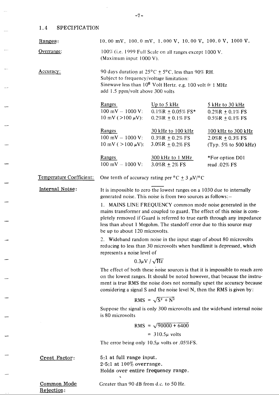
I.4
Ranges:
Overrange:
Accuracy:
SPECIFICATION
10.00 mV, 100.0
10O7,,(i.e.
(Maximum
90
days duration
Subject to frequency/voltage
Sinewave less
add 1.5
Ranges
100
mV
1999
input 1000
ppm/volt
*
1000 V:
l0mV(>l00pV):
Ranges
100
mV - 1000 V:
l0
Ranges
100
( >
mV
mV - 1000 V:
100
mV,
1.000 V,
Full
Scale on all ranges
V).
at 25oC
than 108 Volt
above
+
300 volts
Up to 5 kHz
0.1%R
0.2%R+0.1%FS
kHz
30
0.3%R + 0.2%FS
pV):
3.0%R
300
3.0%R + 2%FS
50C, less
Hertz. e.g.
kHz
10.00 V,
than
limitation:
+
0.05%
to 100 kHz
+
0.2%FS
to I MHz
100.0 V,
except 1000 V.
90%
RH.
100 volt
(4
I MHz
5 kHz to
FS*
0.2%R + 0.1% FS
0.5%R
100 kHz to
2.0%R
(Typ.5%
*For
rcad.02%FS
1000
kHz
30
+
O.l%FS
300
+
0.3%FS
to
500
option D0l
V.
kHz
kHz)
Temperature
Internal
Coefficient :
Noise:
oC
tenth
One
It is impossible to ,rro 6ll" l,o*est ranges
generated
MAINS
l.
mains
pletely
less
than about I Megohm. The standoff
be up
Wideband random noise in
2.
reducing
represents a noise level of
The
on the lowest ranges. lt should be noted however, that because the instrument is true RMS the noise
considering a signal S and the
Suppose
is 80 microvolts
of
accuracy rating
noise.
This noise is
LINE FREQUENCY common mode
transformer and coupled to
removed if
to about 120
less
to
effect of both
the
Guard
microvolts.
than 30
0.3rrV
RMS
signal
l\/W
these
=
is only 300 microvolts and the
per
from
is referred to true earth through any impedance
microvolts when bandlimit is depressed,
noise
does not normally
noise
+F
\A'
t 3 pV/'C
two sources as
guard.
input
the
sources
is that it is impossible to reach
level N,
1030 due to internally
on a
follows:-
generated
noise
effect
The
error due to this
stage
then the RMS is
of this noise is com-
of
about
upset the
80 microvolts
wideband
the
in
source
accuracy because
may
which
given
by:
internal
noise
zero
Crest
Common
Reiection:
Factor:
Mode
RMS
error being only 10.5p
The
5:1 at
2'5:1
Holds
Greater
full range input.
at 10070 overrange.
over entire
than 90 dB
=
v900001Tm0
=
310.5p volts
volts
frequency
from d.c. to
or .05%FS.
range.
50 Hz.
Page 14
-8-
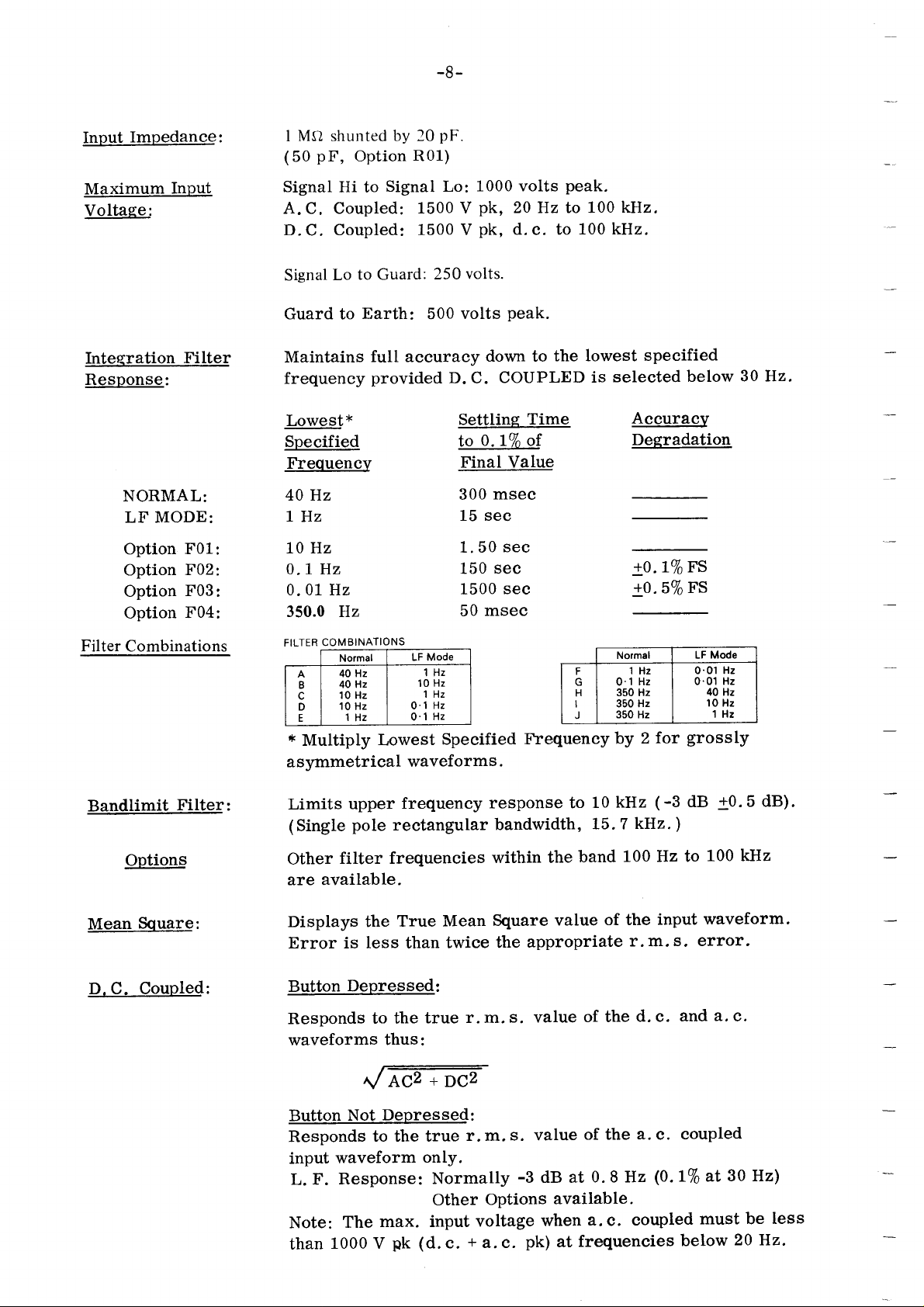
Impedance:
Input
Maximum
Voltage:
Inteqration
Response:
NORMAL:
LF MODE:
Option
Option
Option
Option
Input
Filter
F01:
F02:
F03:
F04:
MO
I
shunted
(50 pF,
Signal
A.
D.C. Coupled:
Signal
Guard to
Maintains
frequency
Hi to
Coupled:
C.
Lo
by 20
Option
Signal Lo:
to Guard:
Earth:
full accuracy
provided
Lowest*
Specified
Frequencv
40 Hz
lHz
L0 Hz
0.I Hz
0. 01 Hz
350.0 Hz
pF.
R01)
1500 V
1500 V
250
500
D. C.
1000 volts
pk,
20 Hz to 100
pk,
d.c.
volts.
peak.
volts
down to
COUPLED
Settlins
0.IVo of
to
Final
300
Value
msec
15 sec
sec
1.50
150 sec
sec
1500
msec
50
peak.
to 100 kHz.
the
Time
kHz.
lowest
selected
is
Accuracv
Degradation
+0.
+0.
specified
below
1% FS
FS
570
30 Hz.
Filter Combinations
Bandlimit
Filter:
OPtions
Mean
Square:
D. C. Coupled:
COMBINATIONS
FILTER
Normal
Hz
40
40 Hz
ts
10 Hz
n
10
Hz
1Hz
E
*
Multipty
asymmetrical
Limits upper
(Single
Other
pole
filter frequencies
LF Mode
1Hz
Hz
10
lHz
01Hz
0lHz
Lowest
Specified
waveforms.
frequency
rectangular
are available.
Displays the
True Mean
Error is less than twice
Button
Responds
waveforms
Depressed:
to the
true
thus:
r. m.
FYequency
response
to
bandwidth,
within the
Square
the
value
appropriate
s. value
F
H
I
J
10 kHz
L5.7
band
of the
of the
Normal
1Hz
01Hz
350 Hz
350 Hz
350 Hz
for
2
by
(-3
kHz.
l-00 Hz to
input
r.m.s.
d. c.
LF Mode
0.01 Hz
0.01
4O
10 Hz
1Hz
grossly
+0.5
dB
)
100
waveform.
error.
a.
and
Hz
Hz
dB).
kHz
c.
Button
Not
Responds
waveform
input
Response:
F.
L.
Note:
than
The
1000 V
Depressed:
to the true
only.
Normally
Other
max. input
pk (d.
c.
s. value
r. m,
OPtions
voltage
+
a. c.
-3
pk)
dB at
when
of the
0.8 Hz
available.
a.
c.
frequencies
at
a.
coupled
c.
(0.
l%o at
coupled
below
30 Hz)
must be
20 Hz.
less
Page 15
-9-
Beadine
Rate:
BCD Output:
Remote
Proqramming:
Power Supplvz
Operating Temperature:
Storage Temperature:
Dimensions:
Internal:
Options
and Function.
code.
provided
are
Option
remotely
logic.
-255
205
Specify
3 readings
(BO
I
BO
,
1-2-4-8
External hold command
for
readings at
(P01):
Enables
progremmed
105-127
V,
/sec.
I a, BO2,
*ve
any range or function to
V, 48
BO2a): Reading,
TTL compatible
True,
print
and
up to 20
using
per
+ve
True, TTL compatible
to 44OHz.
line frequency and voltage when ordering.
Consumption: Approximately 10 VA.
OoC
-25oC
Height: 90
+50oC,
to
to
+70oC.
mm
(3.5")
Width:
224
(9.9")
Range
facilities
second.
be
mm Depth: 330 mm
(13")
Weieht:
Shippine Weieht:
Panel Mountins:
L. 4. L
accuracy is
procedures
periodic
Section 6, MAINTENANCE.
in
Specification
A
checking
check
Verification
routine to ensure that the instrument
given
given
Section
in
suitable for
are
of instrument calibration.
(8.8
4 kg
lb) net
4.6ke(10Ib)
panel
hardware
mounted
Additional
to be
SPECIFICATION
5,
incoming
gross.
is available
in
inspection
Full
enable the
to
rack.
a standard
19"
is working
VERIFICATION.
purposes,
calibration
procedures
instrument
within its
The
for
or
use
are
specified
checking
a
as
given
Page 16
-1
0-
2.r
UNPACKING
Every
instrument will
new
however,
provide,
an
and our
hazards of
orders.
Should
fact will
the
Unpack
panels,
push
immediately.
2.2
INSTA
INSTA
AND INSPECTION
is taken
care
reach
economic
level
LLATION
in the choice
you
in an unblemished
limit
of
the
to
protection
road or rail transport.
your
instrument have
probably
instrument and carefully
the
visible as external
be
buttons, terminals,
LLATION
SE
CTION
AND
packaging
of
degree of
more than adequate
is
packaging/protection it is desirable to
Special export
subjected to
been
damage to
examine
etc. If
any damage
2
OPERATION
materials
factory-fresh
to cater
packaging
is
excessive
shipping carton.
the
the exterior
is found,
to ensure that
condition.
There is,
for all the
provided
mishandling
for overseas
in transit
for damage
notify the
Carrier
your
normal
to case,
Unless
ready
2.2.L
105to
windings
note the
otherwise specified
for immediate use with 205
Voltage
make the instrument
To
I27V,
of the
tags
Tappinss
48to
mains transformer.
mounted
mains transformer.
screws
far
securing the
the
wiring
as
will
series-connected
the
other.
7\
of
440H2, it is
on the
gain
To
panel,
rear
permit.
linking the
by
(
at the time of
to 255 V,48 to
ordering, the
440 Hz supplies.
suitable for operation
necessaryto
Remove the
printed
circuit
board
access to these
and to ease
240-volt
For
fstartr
BLAC K
(Red)
the
operation
of one
105127
U
PP LY
5U
instrument is
from
supplies
normally despatched
in the
alter the connections
top cover
adjacent
tags
panel
it is
away from the
winding
+\
c\
P
(See Section 6.2,)
to the toroidally-wound
desirable to
the two
primary
to the
rfinishf
BLACK
range
primary
the
to
remove
instrument
windings
(Brown)
and
the
four
as
are
ORA N GE
Fig.3 Mains transformer
ORANGE
taPPings
Page 17
-1
1-
Remove
supply
i. e. Red
Orange to
2.2.2
the link and reconnect
is applied across
should
Supplv
As
already
form
joined
be
Neutral
the
Lead and Earthins
described
rstart'
the
to Black
input.
in
fitted with a moulded-on 3-pin
instrument and should
specified
code
When
that the
be
connected
a
cartridge
instrument
in 8S4410.
connecting the
case
to the
supply-line
fuse, this shouldbe replaced by one of
It should be noted
earthed,
measurements
potential,
none of the front-panel
to be
(See
Section
pushed
be
viz. Brown = Live
supply
shouldbe
that although it
made
on circuitry
2.2.3).
parallel
the two
and
form the
to
Section
windings
'finish'
1.2. the
in
of both
input; Brown
Live
2-metre
socket. This fits the
firmlv home. The cable
Blue = Neutral
Green/Yellow
to
a
suitable
lead
earthed via
earth by using a
=
plug,
the YelloVGreen
3-pin
low-current rating,
is recommended that the
terminals
are
connected
floating at a considerable
so that the incoming
windings
supply lead
receptacle
conforms
SuPPIY
plug.
Earth
is strongly
it
If the
the case.
to
shown in Fig. 3.
as
should
is
at
the
to the
joined
be
permanently
rear of the
colour
recommended
earth
wire; this
plug
used
incorporates
say 1or 2 amperes.
instrument case
This enables
level above
earth
to
should
should be
In these circumstances
elevated to
be
can
not
only
suppty mains, but also the
the
covers.
2,2.3 Input
Three
Lo and
Hi,
may be
spacing
f;"
Note:
Signal
FuIl
input terminals
signal input terminals
Guard.
made using
between centres,
following
The
Hi to
D. C.
A. C. Coupled:
SignaL Lo
Guard
detaits
dangerous
Connections
These terminals
4 mm banana
input
Signal
to Guard:
to
of the
and the circuit
Lo:
Coupled:
Earth:
recommended methods of
it should be
potentials.
remembered that the
For this
signal input leads, before
are located
maybe
plugs.
on the
used
The terminals
enabling double or triple
voltages
must not
1000 volts
1500
V
1500
V
200 volts
500
volts
under test
be exceeded
peak.
pk,
d.
c. to
pk,
20 Hz to
peak.
peak.
given
are
internal
reason it is
safest to
removing the
front
as
panel
tbinding-postst,
are
banana-plug
under
marked respectively
mounted on standard
adaptors to
any circumstances:-
100 kHz.
100 kHz.
making connection
Section 2.4.I.
in
guard
shields
disconnect
instrument
or connection
be used.
between
the
Page 18
-12-
2.3
ON/OFF
RANGE INDICATION
CONTROLS
LIGHTS
push
A
at the
isolates the
of the mains
is disconnected.
Although no
so arranged that when
at
when no numerals are
Immediately to the
tights
button
left
least
are fitted to illuminate
switch with
of the display
mains supply live from
fuse
and socket,
one
tSupply
part
On'pilot
of the
right of the
v mV
The legends are
interpreted
be
can
necessary in order
conectly
alternate
above
the input
which remain
the mains
display
visible.
v2
FR
as being
ON/OFF
the instrument,
light is fitted, the circuit is
transformer
will always be
numeric
one of the
uction
terminals.
with
live
unless
display,
following
is mounted
It
completely
the exception
the supply-lead
is energized,
glowing,
four indicator
even
legends:-
mV2
FR
that the
either
numeric
volts or millivolts.
display
PUSH
BUTTONS
A row of eleven
the only
should
it
button
the
SQUARE
RANGE
operational
controls.
be understood
is depressed.
no! depressed.
button
is
Y2
FR
push
buttons, each clearly
the labelled function
that
i.e.
The six
mV2
or
FR
Lest
there
A
TRUE RMS display
push
buttons
1kV 100V
corresponding to
1000.V
Overranse
of the
display
100.0V 10.00V
is signified by
normal
of 1999 except
are rltumlnated
operating
decimal
the
it would
any
be
or
at the
10V
full-range
display.
displays
10070
on the
onlv when
in the tvlean
point position
otherwise
be
marked as to
confusion
range
regarding
becomes effective
is obtained
left of the
lV
row
100mV
of:-
1.000V
a 1 being
100.0mV 10.00mV
illuminated
overrange
1 kV range which
the instrument
is
Square mode to enable
be established;
to
toff
its function,
the
screenr.
are
these
markings,
when
when the MEAN
are marked:-
10mV
at the
permits
is L000
left
a maximum
max.
Overload.
(apart
out
selected.
is
Above
from
100% overrange
decimal
the
point)
1999 the
of
a less sensitive
until
display blanks
range
Page 19
-13
-
REMote
PROGramme
DC COUPLED
BAND
LIMIT
button
This
With the
remotely
be
logic.
normally
played.
When
is
responds to the
a low-frequency
Button
the
of the
this
a.
c.
instrument
Depressing
Iow-pass
filter
is
is effective
button
programmed
Section
See
showing
push
coupled
Depressed:
responds to
signal thus:-
input
this
filter to
-3
dB at
noise bandwidth
frequency
may have
only
depressed,
3.2.
whether
no_t depressed,
button
via a d. c.
a. c.
button
of
is
component
response
Shorts
introduces
reject
10
15.
high
kHz
llllz. Note:
7
been
when
Range and
the
using
of
+ve
range-indication
The
volts
blocking
or
of
-3dB
out the
the
both
frequencies.
giving
fitted
an equivalent
by
Option
millivolts
capacitor.
the
at
blocking
a
(P01) is fitted.
Function
True
d. c.
TTL Compatible
the
input
0.8 Hz.
and a. c. components
single-pote
An
alternative
request.
may
lights
are being
input to the
The instrument
See
(
only,
Section
-6
dB/Octave)
signal
capacitor
Normally,
rectangular
filter
function
dis-
instrument
with
2.4.2.
so that
the
LF MODE
MEAN
mV
SQUARE
NULL
Under
the
is
Button
normal
lowest
40 Hz, with
Depressed:
conditions,
measurement
a settling
for s5rmmetrical
15 seconds.
*Note:
filter
With
frequencies,
the
responds
instead
appear
to
either
V2
details
For
MEAN
to the
of the
the display,
on
or
SQUARE
True
True
mV2
FR
a screwdriver-operated
is
This
instrument
the
zero
with
To
together
range
and
display
BAND
the
lowest
LIMIT to
reduced
possible
adjust
and connect
due
to
input-signal
mV NULL,
note the
to internally-generated
readout.
with
frequency
time
Extends
waveforms*
asymmetric
of
Section
see
button
Mean
RMS value.
the
indicated
as
FR
adjusted
be
applied
strap
them
offset
exclude
reading
the
Then
readout
figure.
push
this
symmetrical
for
msec.
300
of
lowest
the
1Hz, with
to
waveforms
Specification.
1.4,
depressed
Square
of the
enable
To
numerical
by the
preset
minimum
for
to the
most
all three
earth.
true
to
in the
thermal
high-frequency
adjust
mV NULL to
will
It
button
not depressed,
measurement
settling
a
alternative
and
instrument
the
waveform
input
decimal
the
indication
range
control
output
sensitive
input
is,
indication
enable
to
indication
range.
terminals
Select the
window
last
noise.
noise,
and
obtain
possible
be
not
waveforms*
frequency
time of
point
in fact
lights.
10 mV
the
of
Select
note
the
to
Page 20
'L4'
mV NULL
(continued)
}.USE
2.4
OPERATION
Assuming
that
you
strongly recommended
1)
Check that
mains supply
major
voltage ranges
See Section
2)
Connect
the
reduce the readout to
quite
window
becomes 20 - 30 when D01
The supply to
protected
is
type
rating
are
that,
the
is
the mains transformer
by a 20mm x
fuse;
160mA
for I l5V operation.
going
to
before switching
instrument
which it
to
no fine
zero,
rating
for
for 230V operation
normal
use the Model
is
correctly
is to be connected. Within each of the
tapping
2.2.I.
supply
lead
.....
if
an indication of 2
and
a correctly
fitted.)
is
glass
5mm
1030 for
you
on,
adjusted instrument.
primary
cartridge,
windings
anti-surge
and
first
the
should:-
adjusted for the
adjustments are required.
in doubt
see Section2.2.2.
to 3 in the last
(This
250mA
time,
it is
particular
two
3)
Switch
ON the
supply
and, while allowing a minute or
circuits to stabilize, read Section 2.2.3 and Section 2.3 to familiarize
2.4.L
yourself
of the
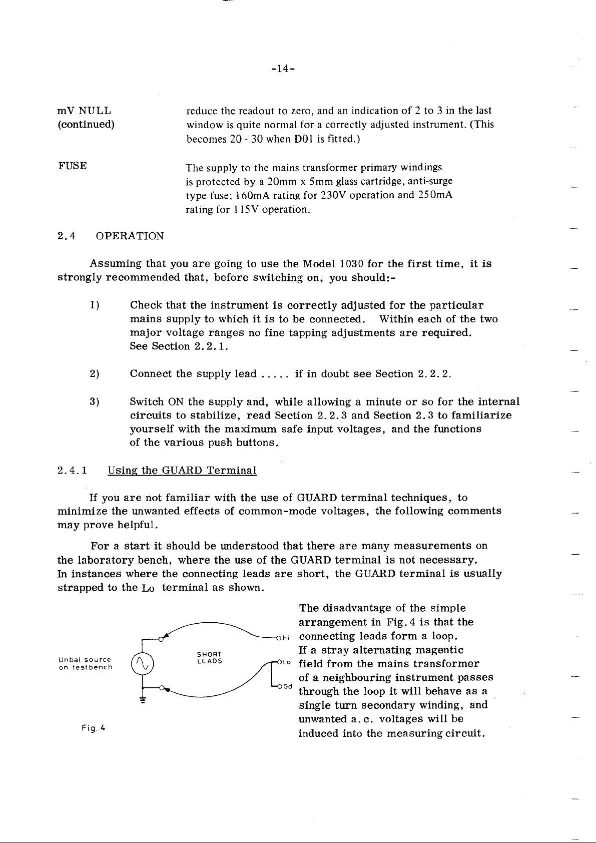
Usine the GUARD TerminaL
you
If
are not familiar with
with the maximum safe input voltages, and the functions
various
push
buttons.
the use of GUARD
minimize the unwanted effects of common-mode
prove
may
laboratory bench, where
the
In instances
strapped to the
For a
helpful.
start it should
where
the connecting
terminal
Lo
be understood that there
use of the GUARD terminal
the
leads are short, the GUARD terminal
as shown.
The disadvantage of
arrangement in
connecting
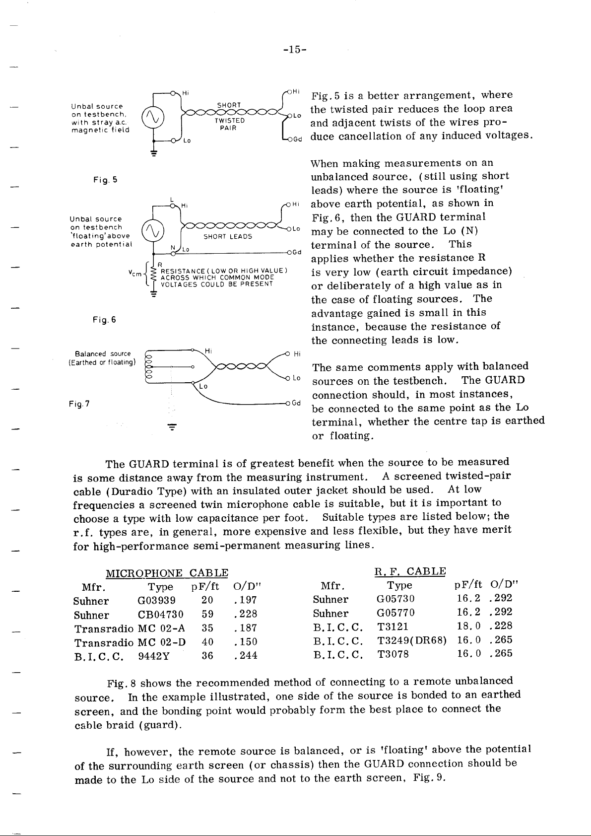
Unbai
testbench
on
source
SHORT
LEADS
If a
field from the
of a neighbouring
through the
single
Fig
4
unwanted
induced into the measuring circuit,
so for the internal
terminal techniques, to
voltages,
many
are
following comments
the
measurements
is not necessary,
is usually
simple
the
Fig.4 is
that
leads form a loop.
stray alternating magentic
mains
transformer
instrument
behave as a
winding,
will be
turn
a.
loop it will
secondary
voltages
c.
on
the
passes
and
Page 21
-15
-
source
Unbal
testbench,
on
ray
wit h sl
magnetic fietd
Unbat source
testbench
on
'ftoating'above
earth
Balanced
{Earthed
Fi9.7
a.c-
Fi9.5
potentral
Fi9. 6
source
floating)
or
"-{
SHORT TEADS
RESISTANCE ( LOW
ACROSS WHICH
VOLTAGES
COMMON
COULD
HIGH
OR
PRESENT
BE
VALUE
MODE
Fig.5
the
and
duce
When
unbalanced
Ieads)
above
Fig.6,
may
terminal
applies
)
is very
or
the case
advantage
instance,
the
Hi
The
Lo
sources
connection
uo
be connected
terminal.
or
is a better
twisted
adjacent twists
cancellation
making
be connected
deliberately
connecting
same
floating.
pair
measurements
source,
where
earth
then the
the
potential,
of the
whether the
(earth
low
of floating
gained
because
leads
comments
on
testbench.
the
should,
to
whether
arrangement,
reduces
of any
source
GUARD
to
source.
circuit
a high
of
is
the
the
the
the
of the
(still
resistance
sources.
small
in
same
wires
induced
using
is
shown
as
terminal
Lo
the
This
value
resistance
is [ow.
apply
most
point
centre
where
area
loop
pro-
voltages.
an
on
short
rfloatingr
in
(N)
R
impedance)
as in
The
in this
of
balanced
with
GUARD
The
instances,
as the
is earthed
tap
Lo
GUARD
The
some
is
cable
distance
(Duradio Type) with
frequencies
choose
r.f. types
a type
are,
a screened
terminal
away
low capacitance
with
general,
in
for high-performance
MICROPHONE
Mfr.
Suhner
Suhner
Transradio
Transradio
C.
C.
B.I.
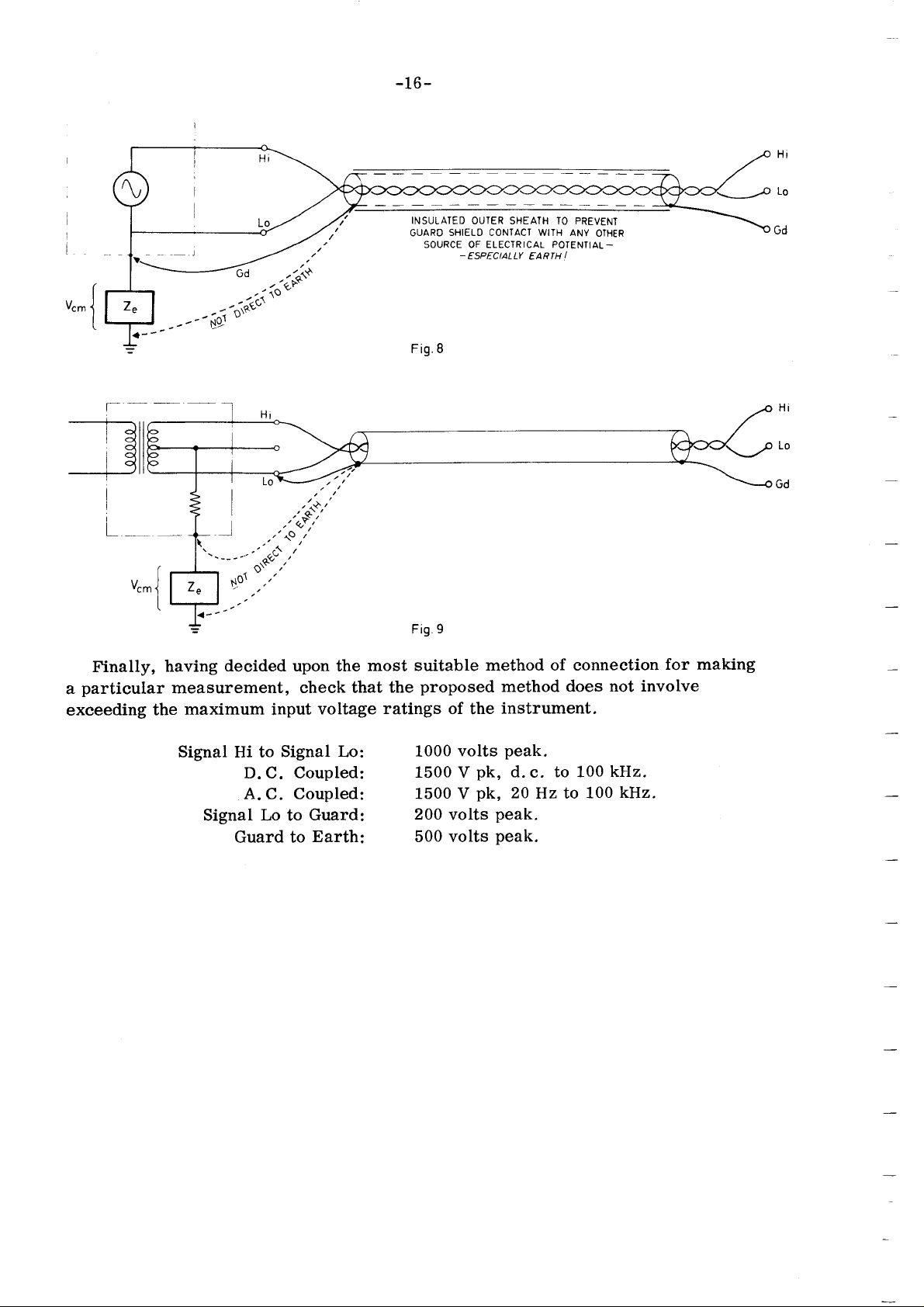
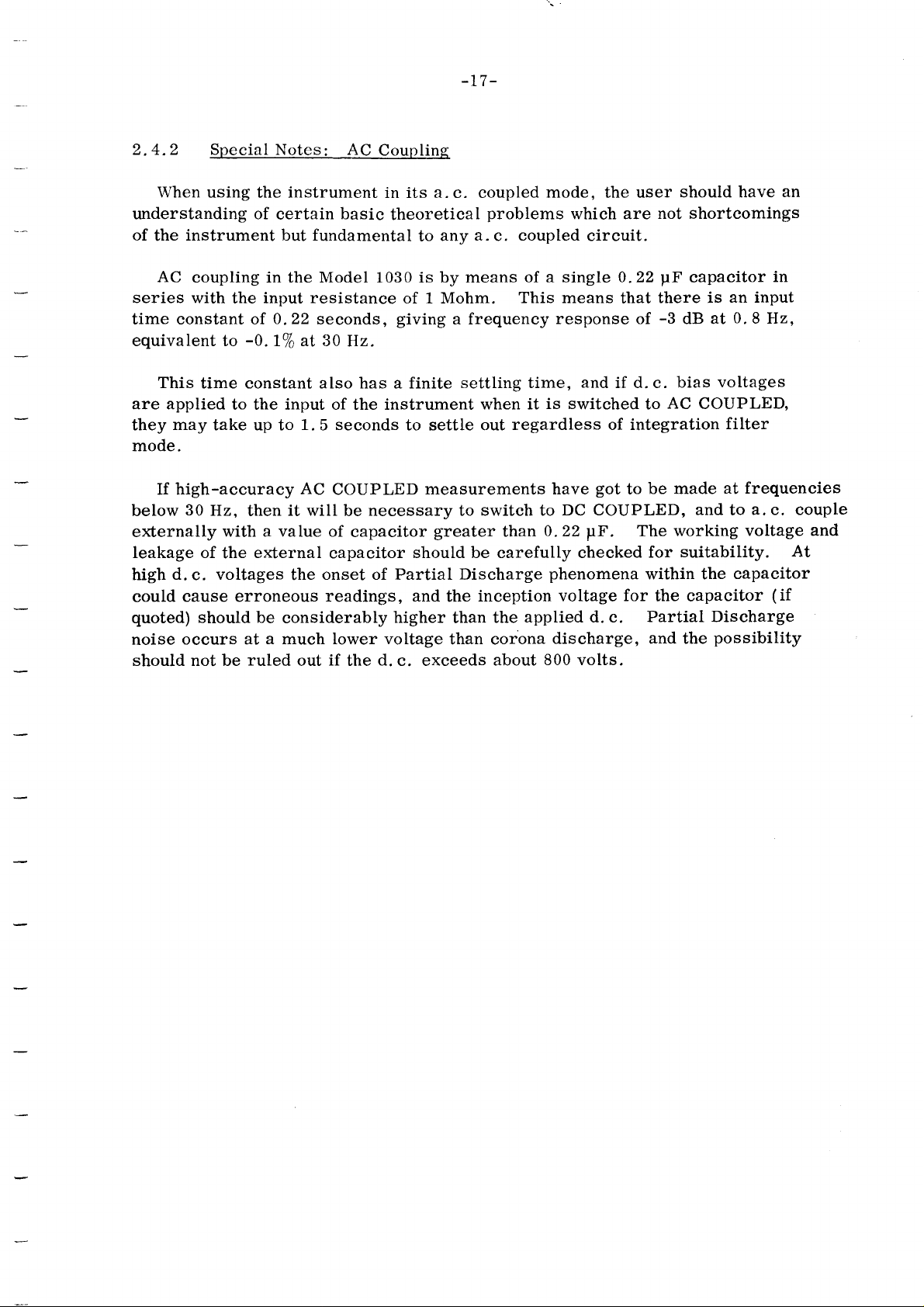
Fig.8
source.
screen,
cable
of the
made
braid
If,
surrounding
to the
Type
G03939
CB04730
MC
MC
9442Y
shows the
In the
and the
(guard).
however,
Lo
02-A
02-D
example
bonding
the
earth
side of the
greatest
is of
from the
measuring
an insulated
microphone
twin
per
more expensive
semi-permanent
CABLE
pP/tt
20
o/D"
.L97
59 .228
35
40
36
recommended
remote
.187
.150
.244
illustrated,
point
would
source is balanced,
screen
source
(or
probably
chassis)
and
benefit
instrument.
outer
jacket
cable
foot.
and
measuring
Suhner
Suhner
B.I. C.
B.I.
B.I. C. C.
method
one
not to the
of connecting
side
when
the
A screened
shouldbe
suitable,
is
Suitable types
less flexible,
lines.
R. F.
Mfr.
G05730
G05770
T3121
C.
C. C.
T\249(DR68)
T3078
of the
form the
then
source
best
rfloatingr
is
or
GUARD connection
the
earth
screen'
source
to
used.
is
it
but
listed
are
but theyhave
CABLE
Type
remote
a
to
bonded
is
place
to
above
Fig.
measured
be
twisted-pair
At low
important
below;
merit
pF/ft
16.2.292
L6.2
18. 0 .228
0
16.
16. 0 .265
unbalanced
earthed
an
to
connect
the
should
9.
to
the
O/D"
.292
.265
the
potential
be
Page 22
-16 -
i
t
(
V..'{
I
\.
u"{
Finally,
particular
a
exceeding
Gd
having
decided upon the
measurement,
maximum
the
-'1O
..a'
,,-a'f
'c.V'
,
-
check that
input
most suitable method
voltage
INSULATED
OUARO
SOURCE OF ELECTRICAL POTENTIAT-
Fig.8
Fig
proposed
the
ratings of the
OUIER SHEATH
SHIELD CONTACT WITH
_ESPECIALLY
9
method does
instrument.
PREVENT
TO
ANY
OTHER
I
EARTH
of connection
not involve
for making
Signal Hi to
D. C. Coupled:
A.
C.
Signal Lo to
Guard to
Signal Lo:
1000
1500 V
Coupled:
Guard:
1500 V
200
Earth: 500 volts
volts
pk,
pk,
volts
peak.
d.c. to
20
peak.
peak.
Hz to
100
100
kHz.
kHz.
Page 23
-17
-
2.4.2 Special Notes: AC
When
understanding of
of
the
AC
series with
time constant of
equivalent to
This
are applied
they
mode.
If high-accuracy
below
externally
leakage of
high
could
quoted)
noise
should not be
using the instrument
certain
instrument but fundamental
coupling in the Model 1030 is by means
the input
0.22
-0.
l1o at 30
time constant also has a finite
to the input of the instrument
may
take up to
30
Hz,
with a value of
the
d.
voltages
c.
cause erroneous readings,
should
occurs at
it will
then
external
the
be
considerably
a much lower voltage
ruled
basic
resistance
seconds,
Hz.
1.5 seconds
AC
COUPLED
be necessary
capacitor
capacitor
onset of Partial Discharge
if
out
the
Coupling
in its a.c. coupled
theoretical
any
to
of 1 Mohm.
giving
to
settle
measurements have
greater
should be carefully checked
and
higher
d.
c. exceeds
problems
a.
c.
a frequency
settling time,
when it
out
to switch to
inception voltage
the
the
than
than corona
about
mode, the user
coupled
of a single 0.22 yF
This means
response of
is switched
regardless of integration
DC COUPLED,
0.221tF.
than
phenomena
applied d. c.
discharge, and the
800 volts.
which are
circuit.
that
and
if d.c.
got
to
The
for
should have
not shortcomings
capacitor
there is
-3
dB at
voltages
bias
AC
to
be made
for
within the
Partial Discharge
COUPLED,
at frequencies
and
working voltage
suitability.
the capacitor
possibility
in
an input
0.8llz,
filter
a. c. couple
to
capacitor
(if
an
and
At
Page 24
-1
8-
SE
C TION 3
OPTIONA L REMOTE
3. 1
OPTIONS
(BO
I ) and
(BO
I a) : I
-2-4-B
3.1.1 Description
(BO
Options
Reading Range
I ) and
and
RIBBON' Connector
earth
and
also
from
(BO
I
enable full Binary
a)
Function to be obtained
(J5)
mounted on the
from
rear
the signal input terminals.
panel.
Whilst it is recommended that the output digital
earth,
earth and
enabling
the input terminals
digital common.
The
50-way connector
complete
levels are TTL
external control of the
compatible,
may be floated
also
provides
(J5)
with a fan-out of 4.
as high
Analogue
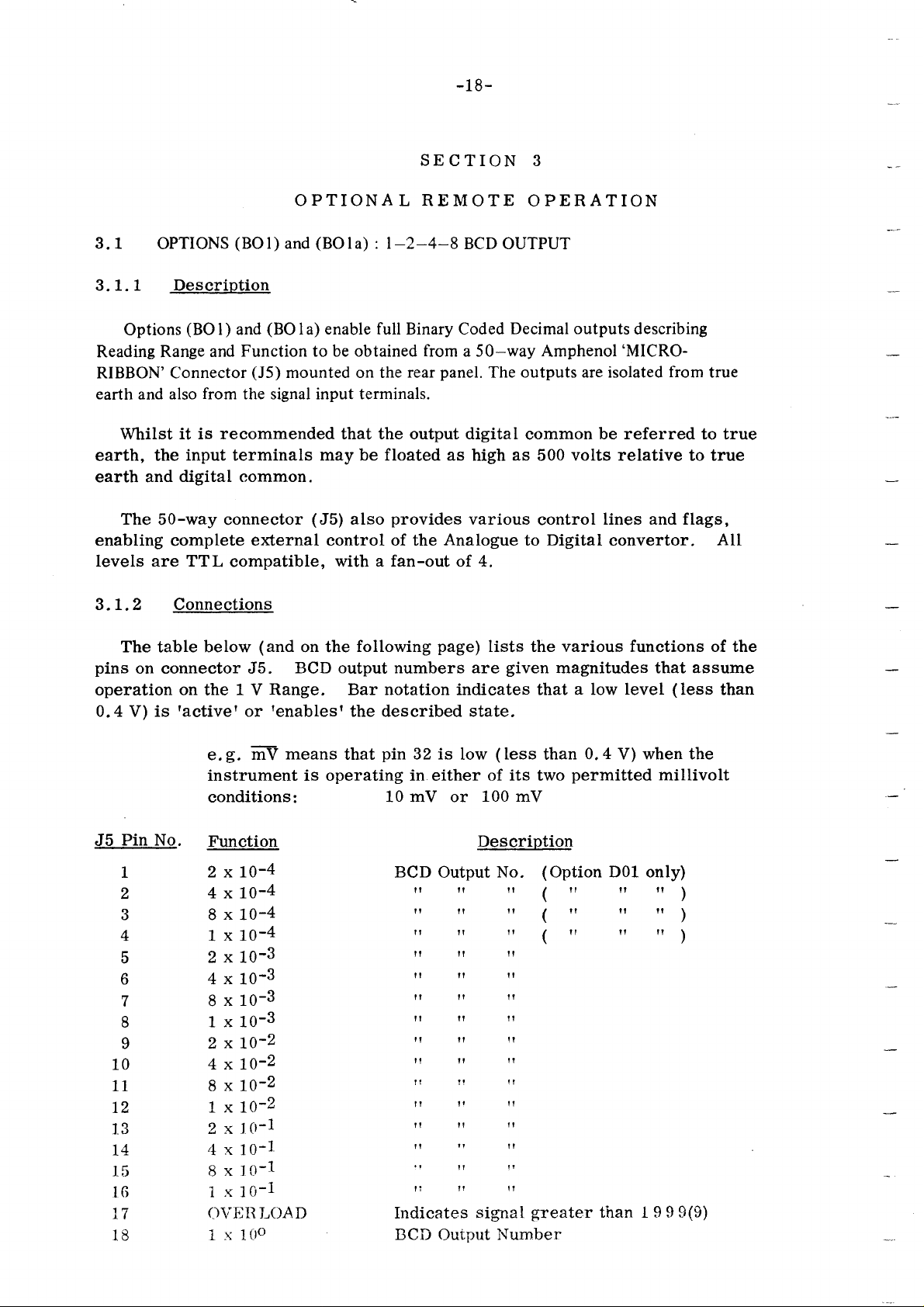
3.I.2 Connections
The
table
pins
on connector J5.
below
operation on the
0.4 V) is
ractivef
(and
on the
following
BCD output numbers are
1V Range. Bar notation indicates that a low
renablesr
or
the described state.
page)
OPERATION
BCD OUTPUT
Coded
Decimal
outputs
describing
a 50-way Amphenol'MICRO-
outputs are isolated
The
as
various
to
common
volts
500
control
Digital
be referred
relative to true
lines and flags,
convertor.
from
lists the various functions of the
given
magnitudes that assume
level
(less
true
to true
All
than
e.g.
instrument is operating in either
conditions:
Pin No.
J5
I
2
Function
2 x 10⁻⁴
4 x 10⁻⁴
3 8x10⁻⁴
4 1x10⁻⁴
5
2 x 10⁻³
6 4 x 10⁻³
7
8
I
10
8x10⁻³
1x10⁻³
2 x 10⁻²
4 x 70'2
11 8 x 10⁻²
72
l3
L4
15 8
16
17
18
1 x 10⁻²
2 x
4 x 10-1
x 10-1
.x
i
O\IERI-OAD
i r 1{)0
frT
l(r-1
10-1
means
that
pin
32 is
10 mV or
low
of its
100 mV
(less
than
permitted
two
0.4 V) when the
Description
(Option
BCD Output
rrrrrt(rrilrl
rr rr
niltt(tfrtrt
ilil?t
ilntl
ll ll ??
?t t? ?t
|lilil
t!
?r ?!
l?
ilIttt
It
.r
fi tr l?
Indicates
BCD
Output
No.
lr
Ir
rr
tl tr
signal
Number
tt
t?
rl
tt
ll
greater
(
D01 only)
rr ?r rr
than l9I9(9)
millivolt
Page 25

Pin No. Function
J5
-1
9-
Description
19
*
20*
2l
22
*
*
23*
24*
25*
26 Not
used Do
27 Not used
28 MEFxI@RE
29 DeETiPtE'D
30 BTND-LIfim
31
32
33
34
35
mTfOTE'
niv
Not
used
RANGE A
RANGE B
36 RANGEC
37
38
39
40
4L
RANGE D
Not used
Digital COMMON
FOID Input
ffi'
42 FE'NrfrEIFrr
43 SIG.
44 DEffi
4s
46
47
48
49
50
INTEGRATE Output
ffi output"
+
)r
t
*
I
030 Range Coding
*
Used for
programming
when Option ( P01)
not
connect
Do not
r0r
r0'
'0f
'0'
'0r
Do not
Decimal Point Coding
)
(Range). (See
)
tables)
)
(Option
)
Do not
tOt
Input
connect
indicates
MEAN
indicates DC
indicates BAND
indicates
LF
indicates mV:
connect
following
BOI and BO2 only)
connect
state reference
control
rr ?t ?t
??
'?
"
rt
line
flag
line
flag
*
Used for
when
for
Options
programming
Option ( P01) is fitted.
BO I a and BO2a
Ranges and F\rnctions
is fitted.
SQUARE:
COUPLED:
'1,
r1r
=
LIMIT: f 1, = WIDEBAND
'1r
MODE:
tf
indicates Volts
=
NORMAL
',
Ranges
=
RMS
AC
COUPLED
and
Functions
Range
0mV
00mV
V
OV
00v
000v
Range
lOmV
l00mV
IV
l0v
l00v
1000v
1030
Pin
34
(A)
Pin
Pin
I
0
I
0
I
0
Range Coding for Options
34
I
I
0
I
I
I
(A)
Pin
35
0
I
1
0
I
l
(B)
(B)
35
0
I
I
0
0
I
BO I and BO2
Pin 36
I
0
I
I
0
I
t
Pin 36
(C)
-
(C)
BCD Output
0
0
0
I
I
I
aa
(D)
JI
Pin
I
I
I
I
I
0
Page 26
-20-
3. 1.3
Suppose the following
this
Pins
3 8x10⁻⁴
5 &6
g
8r
15 &
Now suppose
low or'O'
Examples of BCD Codins
gives
12
16
Pin 32
Pin
rieht
The
a reading of:-
+2
x10-3
+2xI0-2 +
+8x10⁻¹
that Option
(less
state
low, indicates
35 and
reading is
36 low, indicate
ie. 10.00(0)
therefore
than
pins
of J5 are in a
3-5-6,9-r2-15-16
=
0008
.
+4x10-3=.006
x 10-2
1
+1
x10-1
TOTAL
BOla is
0.4V):
that the instrument
9.368 millivolts.
=.03
=.9
=
.9368
fitted and
that the
decimal
rlr
(
Option D01 only)
pins
that
is measuring
point
state
32,35
is one
(greater
mV.
and 36
place
than2.4
are in
to the
V):-
a
Alternatively,
pin
If
Alternatively
37, may be
and
Pfns
do not affect
and
when the
present
though
even
they
mV may be interpreted as
28 had been held
when
30 and 31 are merely
29,
interpretation
input
signal
when
will be
pin
regarded as
or
is
too
pin
1? is in a
accurate
.9368
=.
at
e.
28 is
.
high
for numbers only
x 10
1000
009368 volts
tOf
,
s68
hetd
squared,
9368
(
1000)2
00009368 V2
of
for a
'1f
the output
then
S#
at
x ( 10)2 volts2
flags indicating
BCD number.
the
particular
state but thev
'0f
rdivided
(FR
weighting
the
giving:-
slightly
by 1000r
would have
=
range.
Range)
Fult
partieular
a
Pin
must
in exeess
of
17, OVERLOAD,
BCD numbers
giving:-
been:-
pins
not be taken
34, 35,
32,
measurement
may
of 1 9I9
(9).
36
mode,
indicates
be
vaiid
as
3. L.4 Control
40
Pins
remotely
system.
be held
can
when it
45 are control
to
The
control
a
to
Lines
lines, enabling
is
used in conjunction
lines float to a
state by
'0'
or low
input
the user
with other equipment
'1'or
connecting
high
them
to control
as
state if open
pin
to
39,
instrument
the
part
circuit,
digital
a test
of
and
COMMON.
Page 27
-2t-
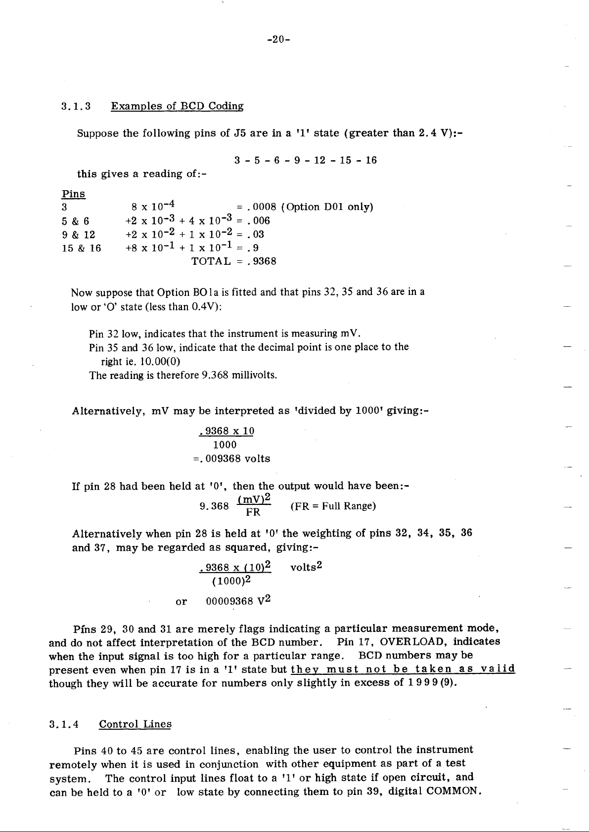
3.1.4.1 Print Command:
state at the end
ferred to the
steady
BCD output information.
The
storage registers
falling voltage
of
measurement
each
step
Pin 45,
m
cycle,
when
and is available at the
available at
pin
45
reading device to take note of the BCD output or,
be used
it is available at any time
Pin 45 is in
to inhibit scanning of the BCD information.
the'l'
except when new
for approximately 5mS during
stafe
information is being transferred.
occurs.
A
logic low on
pin
occurring
forced to
3.1.4.2
on
a low state in
Sisnal Intesrate:
digital convertor
represents the earliest
edge
to the input
operate
to
accurate
via
its
terminals
a signal
information.
delayed command
pin
42 FE'Ni?trINEiEfI
45,
thus making it easy
this condition.
Pin 43
exhibits a high
is acquiring its information. It is
time at which new
without
disturbing
scanner, for example, at the highest
The falling edge can
facility,
at
the
prevents
stop
to
reading in hand. It can
the
also be used to command
same time.
falls from a f lf
new reading
the
pins
of
can thus command
alternatively,
which
Since
time the update of data
the reading is
has been trans-
in the form of
J5
an external
?1r
the
state can
the ffi
external
printers
etc. Pin 45
state flag while the analogue to
made available because its falling
signal information
may
be
thus be used
possible
speed
for
the instrument,
See Section
3.4. 1.5.
rot
to
stored,
edge from
is
applied
futly
3.I,4.3 Hold
if
is desired to the
it
pin
When
40
followed by
an external
3.L.4.4 Read
instrument
low.
held
progress
in
Readinq: Pin 40,
is taken low the
storing and displaying it until
read
command
Command: A falling edge on
to take
The instrument inhibits commands that
is
complete.
PRINT COMMAND
COMMANO
INTEGRATION CYCLE
SIGNAL
INTEGRATE
mtD,
stop the instrument from
instrument will
is applied
reading
one
the integration cycle.
to
immediately
Fig.10
shows
may
externally
be
held in a low
reaching its normal
reading in
complete
pin
40
is taken high
pin
if, and only
relationship of COTIilIEN-D
the
any
or released, or
41, CIOIIINIAFID,
pin
if,
applied before
are
40
state
free-run mode.
progress,
until
instructs the
already
HOLD
is
conversion
and
PRINT
*
Note:
COMMAND
Minimum
COMMAND
pulse
Fig l0
width
2 microseconds.
is
Page 28
-22-
3.I.4.5
an external
delayed
Delaved
Command:
command is applied,
period
by a
of
time equal
This delay is automaticalLy
is selected by
Provided
at the
A
same instant
particularly
front
the
pin
useful
with a signal scanner,
scanner,
the
INIEGRATION
as for
CYCLE
panel push
44
is
held low,
that new
example
the
eommanding
If
adjusted
signal
of
this is where
same
command
a reading
pin
44,
DELAY is
then
the command will
to the settling
depending
button,
this
or by optional
means
information
being used for stepping
be
to
NFI AY TIMF >T
held at logic
be automatically
time of the integration
on whether
that
the instrument
is applied
the Model
NORMAL
remote
to the
1030 is
programming.
front
used in
taken, Fig.11.
,0r
while
filter.
or LF MODE
be
can
commanded
panel
conjunction
switching
or
terminals.
SIGNAL
PRINT CON4MAND
For
falling
COMMAND
INTEGRATION
SIGNAL
INTEGRATE
maximum read rate
edge of
CYCLE
INTEGRATE
pin
43, SIGNAL
'_-
in
a closed-loop
TIME
DELAY
Fig.1l
system,
INTEGRATE,
the
Fig.12.
command
could be the
PRINT
COMMAND
Fig.l2
Page 29
-23-
3.I.4.6
refemed
minimum
3.2
(BOla)
and
PRINT INHIBIT,
42,
forced to a'third'
bus-bars
or
42, electrically
outputs
single-pole
printing.
for
3.3
r0r
digital
to
fan-out capability
OPTIONS
Options
respectively.
instrument
The
in
of several
switch could
OPTION
State Reference:
COMMON
on
is 4 TTL loads.
(BO2)
(BO2)
all active
state
a system and then,
disconnected
instruments
(
P01): REMOTE
(BO2a)
and
(BO2a)
and
basic difference
The
BCD and control
which
is a
can therefore
be used to
very high impedance
at wiII.
All
digital outputs
pin
39.
Maximum
: THREE
are 3-state
by the
are connected
PROGRAMMING
STATE
(or (Tri-state'*)
is that upon
lines are
permanently
be
application
Another example
select the
and eommand
fan-in
LOGIC
application
inhibited.
OFF state.
parallel
in
outputs
is
OUTPUTS
versions
The
connected
single logic
of a
would
to a
from a
lines are
TTL loads,
two
(BO
of
Options
of a logic
output lines
to
be
printer:
particular instrument
low to
logic highways
where the
I
are
f
0r
to
a simple
)
pin
pin
BCD
3. 1
3.
remotely
Description
Option
(P01)
programmed
programme lines
terminals
programme
system; the
earth
to
3.3.2
push-button
basic
apply
switches.
eould
by means
common
signal
and digital
Method
optional
The
switches,
instrument,
+15
volt
levels
These
present, relays.
be
Similarly,
digital
points
COMMON
Function
and
enables
all Ranges
via the 50-way
are eleetrically
of opto-electronic
(digital
COMMON)
input terminals
COMMON.
of Operation
Programme
making
signal
appropriate
to
are either
connection
switching
field-effect
See
digitat
to
switching
appropriate
lights on the
and
Amphenol
isolated
are then
Board
mounts on
accomplished
is
parts
Drawing
accomplished
is
parts
of the circuitry
display.
Functions
frorn
isolators.
referred
be
able to
to certain
of the
transistors
439105,
No.
of the
connector
both earth
recommended
It is
earth in
to
float
of the
top
of the contact
by the
analogue
or,
Sheets
by the
operate
to
Model
provided.
signal input
and
the
volts
1500
front-panel
push
buttons,
circuitry
where
push
high
2 and
1,
buttons
the
All
that
be
the
the
1030 to
measurement
peak
relative
of
bank
pins.
In the
which
operate
to
signal
voltages
3.
which
decimal
apply
Operation
digital
instead
COMMON
into
No.40911-?.
tines
(output
COMMON.
of
lines
Programme
the
Remote
contacts
tights
This
*
Trade
REM
the
from
programming
of the
up the
mark:
PROG
rest of the
the
Board
push
button
seleeted
National
push
button
mounted
achieved
is
switches),
F\rnction
Semiconductor
disconnects
switches,
on top
of the
by connecting
via connector
lights
both
lines being
the
switches.
decimal
and
Inc'
+15
ths
routed
See Drawing
appropriate
the
J5, to
point
volt and
digital
directly
Page 30
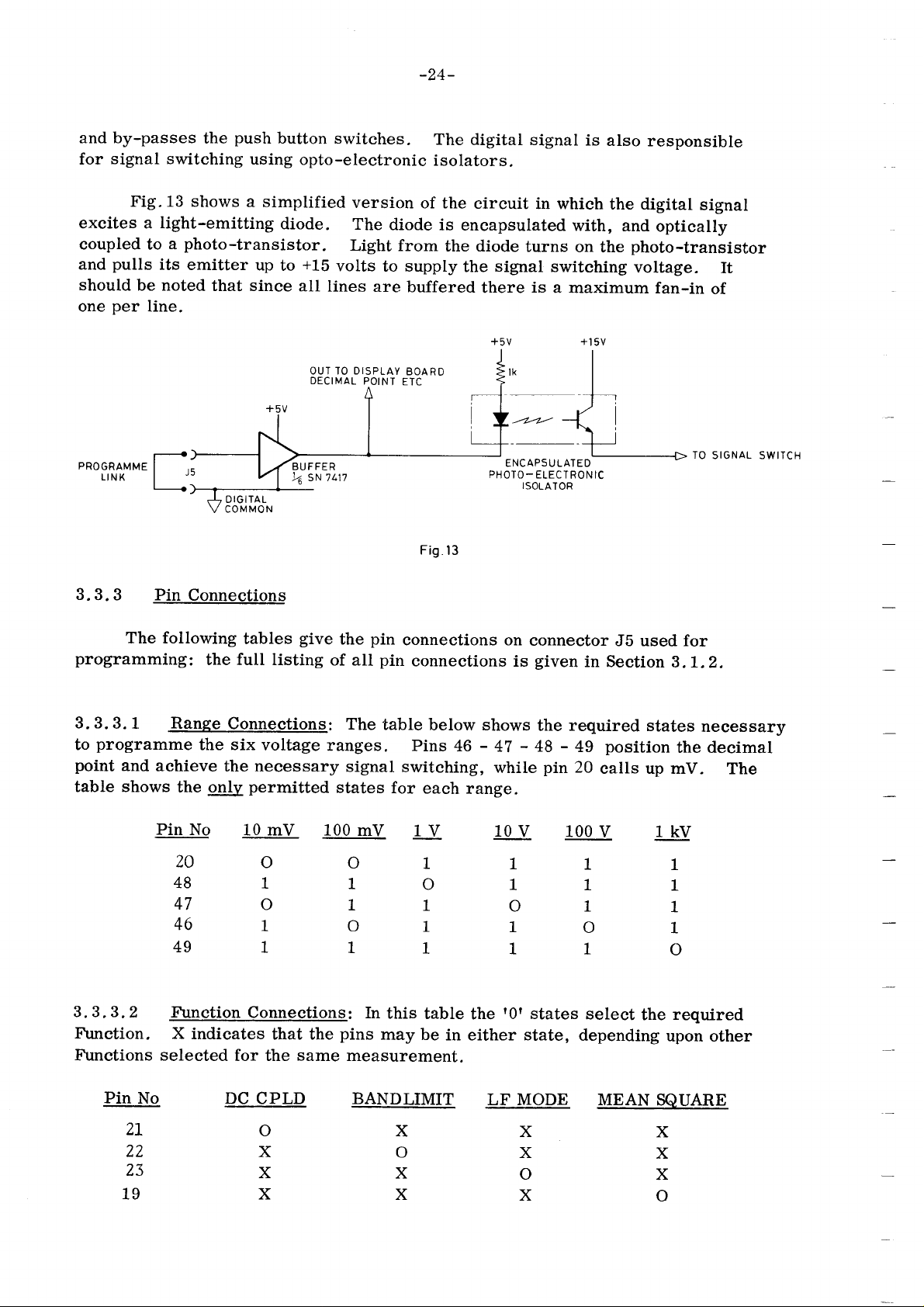
-24-
and by-passes
signal switching
for
Fig.13 shows
excites a
coupled
pulls
and
should
per
one
PROGRAMME
LIN
light-emitting
a
to
its
be noted
line.
K
photo-transistor.
the
emitter
that since
OIGITAL
COMMON
push
button switches.
using opto-electronic
a simplified
diode.
up
+15
to
all
BUFFER
4sN7tt7
version
The
Light from
volts
lines
are
OUT TO DISPLAY
DECIMAL
POINT
The
isolators.
of the
diode
to supply
is encapsulated
the diode
buffered
BOARD
ETC
Fig.l3
digital signal
circuit
the
there
in which
turns on
signal
PH
OTO
switching
is
a maximum
ENCAPSULATED
-
ELEC T
ISOLATOR
is
with,
+l
5v
N IC
RO
the
also
responsible
the digital
and
optically
photo-transistor
voltage.
fan-in
signal
It
of
TO
SIGNAL SWITCH
3.3.3
Pin
Connections
The following
programming:
3.3.3.1
prograrnme
to
point
and achieve
table shows
Pin No
the fuII listing
Range
the six
the onlv
20
48
47
46
49
3.3,3.2
F\rnetion, X
F\rnctions selected
Function
indicates
tables
give
Connections:
voltage
the necessary
permitted
10mV
100mV
pin
the
The
pin
table
of all
ranges.
signal
states
connections on
connections
below shows
Pins 46
switching,
for each
1V
o01
110
o11
101
111
Connections:
that the
for the same measurement.
In
pins
this
table
may be
is
-
47 - 48
while
range.
10v
1
1
o
1
1
rOt
the
in
either state,
connector
given
the
required
-
49
pin
20
100
in Section
calls up mV.
v
1
1
1
o
1
states
select
depending
J5 used for
3.1.2,
states
position
1kv
1
1
1
1
o
required
the
upon other
necessary
the decimal
The
Pin
2I
22
z3
19
No
DC CPLD
o
x
x
X
BANDLIMIT
x
o
X
X
LF MODE
X
X
o
X
MEAN
SQUARE
x
x
x
o
Page 31

4 Characteristics
3
.3 .
of
_25_
Use
As described
a logic
If any
be
for example,
but no
Functions
vaIid.
have been
3. 3. 5
front
the
a
low
line is
The table
obtained.
decimal
The table
may usefully be employed
should be noted that the codes
It
made
Remote Indication
An output code
panel
instrument
f
0'
that
it is
in Section
(less
not
in
Damage is unlikely
all lines high will
point
in
identical to
REMOTE
is
switched
0.4
than
connected,
Section 3.3.3.1
be illuminated.
will
Section 3.3.3.2 indicates Function
appears on
push
switched
for local
3.2
a Range or
V relative to digital
it will
place
facilitate
pin
button
REMOTE
to
float
must be
occur
to
simultaneously,
24 of J5, to
is depressed.
operation
a logic high or
to
adhered to if sensible
if forbidden
instrument
the
for both
svstem
programming
for
via the
Function is
COMMON) to the appropriate
programming
checks.
indicate
Arlron
front
called
rlf
codes
in its l volt
programming,
any combination
and BCD
whether
pin24
via connector
panel
by
up
state.
results
programmed:
are
analogue
or
indicates
push
buttons.
connecting
and
of codes
output
not the
J5,
line,
are to
range,
since all
is
that
This code
use. If
commands
local
programme
pin
operation.
24 is
if
the
lines
be usefully
can
connected
Model
If Option
would be
1030 is inadvertently,
emploJgg-ls
pin
to
(802)
disabled under
42 PRINT INHIBIT,
is fitted, then
-prgvide
or
this condition.
a safety inhibit
intentionally,
output
all
then it
lines as
in
inhibit
witl
switched for
well as
systems
print
Page 32

4.7 GENERAL
_26_
SE
CTION 4
TECHNICA L DESCRIPTION
internal
The
boards. The
D.C. Conversion
to
convertor.
Digital Conversion
to
7-segment
components
For the
and
each
4.2. A.C.
The second board
display devices. In
are mounted
purposes
board
TO D.C. CONVERTOR
of Model
board
includes the
produces
first
circuits
printed
and
and
on the
of explanation the two boards will be described
further sub-divided according
(Assembly
Drawing No. 409106)
1030 are
(Drawing
preamplifier,
(Drawing
the
No.
BCD
the
Model 1030,
second board.
divided
409106)
No.
scaling
409109)
output together with drive
regulated
the
to the
various functions
- - -*
or"*i^r
I
t"
l3glos-rh""J
I I
ot"*ino
No
43e105 sheet
2
l---.---ll,-
between two
is
concerned
circuits,
is
concerned
power
printed-circuit
with
A.C.
andthe
with
for
r.m.s.
AnaLogue
the
supply
separately,
involved.
Lo
l*l
iv
ri-
lo-r I
lcd I I
II
tl
|
t'
+---+
*'
V,
--T
J&|y$iR
PSU
arrenuaron
ATTE NUATOR
-
----+
swrTcHrNG
LINES
I
r- t- trt-l ll
coueLeol^
oc
Lo:vrsl1119u
lo lo lo lo lo lo lo
l^
l^
l"
sheet
l^ l"
3
l^*o*ott
Fig. 14 Schematic
T-
"
|
l^
SWITCHING
diagram of
CONVERTOR
e\l/lTaHt\tn tt\ttrQ
aaruo
LiMIT
CONNECTIONS
A.C. to D.C.
NT
CURRE
TO
VOLTAGE
Convertor
-
Z
HIGH
I
NPUT
BUFFER
AMPLI F IER
3- POL E
INTEORATION
FILTER
,____J
|
Page 33

-27 -
4.2.7
amplifier
are used
normally
(f.e.t.
1 V RANGE
Preamplifier
(Circuit Diagram
The simplified diagram, Fig. 15,
and scaling
(black
ropen')
or by
)
triangular
regardless
means
position
nn
Scalinq
&
circuit. For
contact
of relay
439105
No.
shows
the
normally
of whether
contacts. In
Sheet
purposes
switching
the
Fig.
1)
the essentiaI features of
of
?mader,
explanation
white
is accomplished
15 all switching is shown in
1l0k
et7
$
pre-
the
same symbols
the
triangular contact
electronically
the
The various
VOLTS
RANGE
10
mV
100 mV
1V
10 v
100 v
1 kv
Although
configurations
further,
Fig.16.
Then, having
Circuit
to
OVERALL
voLTS
100
10 (+20
1
0.1
0.01
o. 001
and
Diagram No. 439105, Sheet 1, for a more detailed explanation,
Fig.'15
switching
Simplified diagram
combinations
RELAY FET
GAIN K2
(+40
dB)
dB)
(odB)
(-20
dB)
(-40
dB)
(-60
dB)
reader could, no doubt,
the
on each
show separate drawings
to
grasped
9-8 OPEN
9.8
9-8
9 - 8
9 - 10
9 - 10
range;
it will be
basic essentials, reference
the
of
for
the
Q12
OPEN
OPEN
CLOSED
OPEN
CLOSED
puzzle
quicker
for each
preamplifier
different ranges are as follows:-
FET
Q13
OPEN OPEN CLOSED
OPEN CLOSED CLOSED
CLOSED OPEN OPEN
CLOSED OPEN OPEN
CLOSED OPEN OPEN
CLOSED
out
simplifythe circuit
to
RANGE setting as
the
different
and scaling
FET FET
Q14
OPEN OPEN
circuit
should next be made
Q17
still
shown in
Resistors
990
kohm,
permanently
resistors are
resistance
chain
A
capacitor,
for
frequency
is
1 kV
d. c.
C4. Relay
R1 - R4, in a series-connected
connected to the Hi input terminal.
used in order to
optimum
accuracy on the high-voltage
corrected
working
K1
provide
by
components
polycarbonate
the best
capacitor
by-passes C4 via contacts
chain,
possible
C1, C2
is used
have a total
value of
Four separate
voltage coefficient
ranges. The input
and R115.
for the d.
-
10, 6
9
c.
-
7, when
of
resistor
blocking
the
Page 34

-28-
VOLTAGE
1 VOLT
RANGE
VOLTAGE
100mV RANGE
1OOV RANGE
GAIN ]
]O
GAIN
xl
OVERAtt VOLTAGE
GAtN
+100
VOLTAGE GAIN
VOLT
IO
10mV RANGE
lKV
RANGE
VOLTAGE
+100
RANGE
+IO
1OO
GAIN
+10
OVERALT VOLTAGE
GArN
+1000
switched
instrument
is
via switching-transistor
push
front-panel
across the
relay
button
suppresses switching voltage
coil
of the coil.
is applied to the
R8 and
(990
-
L0 V simplified diagrams.
with R8, is corrected by
unity.
1 kV RANGE
9
attenuator
in this configuration,
define the
R1
parallel
signal
-
R4
10 mV
The input
10 kohm resistor
via
resistors
shown
(
on the
1 Mohm) in
fractionally below
R7.
c8,
On the
transistor
'divide
a
With
the circuit
100 V and
contact
Q2;
100' input
by
resistor necessary to
Rl0
give
frequency comection.
and
network of four diodes,
gate
the
of
input FET
the
Fig.16
turn,
mode.
voltage controlled
the DC COUPLED
to
which is,
Q1
in
or by external command,
gate
dual field-effect
of
normally-closed relay contacts
kohm)
plus
R8
(10
kohm)
reducing the
Frequency
is
connected
correction
positions,
relay
to 0 V, converting
in
which
R1 - R4
resistors
CR4
-
CR7
gain
of the
In
provides
preamplifier.
the event
shunt
a
Q4A.
The
relay
is energized
from the
Option
(P01).
surges due to the
Diode
inductance
transistor
CRl
Q4A
K2 I - 8. Input
form the
l Mohm input resistor
A slight error, due to R9/11
gain
of the amplifier
applied
is
K2
forms the
R9/11
gross
of
path
across R8
is energized
R8 into the
series arm.
provide
the
Components
over-voltage
for the
signal, and
by components
via switching
shunt arm of
1 Mohm input
C5, C6
a
protection
protects
Page 35

-29-
FET
Dual
a type
specially chosen
and thermal
transistor
Selected Value)
To correct
resistors
resistors
give
to
a balanced
balanced
driven
from the
Q4A/Q4B
charaeteristics.
Q5A/Q5B
resistors
for long-term
R152. R153
R16 and R26
pairs
of
collectors
by complementary
may be
and
selected
a
in thermal
be
are cemented
series-connected
of
dismissed
matched
contact
together
output transistors,
resistor R154
FSV
I V RANGE,
tlre
on
circuit
is switched
into
is
connected
for its low noise
The
and the two halves
R21 and
slight
and the
of
mV NULL
Q4A
and
state with the
as a balanced
and
halves
two
of
the
R30.
changes
control
Q4Bl
FSV
mV NULL control
direct-coupled transistors
Q5A
Q11.
other.
same
to
during
serves
Q3.
and
Q5B,
This
Q32
reason.
prevent
crossover
manufacture
a similar
of
pair
with
pair,
and
Q10
relatively few comments.
cemented together
with each
for the
diodes.
and
Q10
Q11
is selected
r R22
resisto
and
by transistor
CR14 and CR15,
long-tailed
close
matching of both
are direct eoupled
circuit
in
the
balanced
balance
by
of the
are connected
resistors
Q6 - Q7,
final
the
part
of the circuit
R17 and
its mid-position.
in
Q8 - Q9,
output
at TPI being
Transistors
with cyanoacrylate
and
Q33,
Forward
used to
is
although
voltage
forward-bias
distortion.
for best
function
flatness
on the
10
pair,
and is of
electrical
dual
to
FSV ( Factory
preamplifier,
across
the
R25 are
Q32 - Q33
quite
is
conventional
and
Q6
adhesive
specially
not
across the
drop
the
response
of
V RANGE
drain
chosen
Cascaded
are
produced
are
Q7
as
so
to
matched,
pair
complementary
1 MHz
at
it
when
The rest
networks
RANGE
switches.
Field-effect
so
it
to the
with
it
that
is turned
the
On
gate
the
at unity.
preset
and
On the
'divide
to
CRl0.
via
or
across
and
the
defining
of the circuit
into circuit,
transistors
permanently
is
by
off
RANGE the
1 V
input
of
1 Mohm
Capacitors
resistor
10 V
10r,
by
Resistor
1
Mohm
gain
the
provide frequency
adjustment.
Reference
100 V
and
1 V
introducing
gain
having
1kV
gain
a
RANGE
tdivide
of
to
RANGES
'divide
a
of unity
when the
by
devoted entirely
is
in accordance
or from
remote
are used
for
conducting
switching transistor
feedback
FET
Q4A.
input
resistor chain,
C14,
R40 enables
and 1
kV RANGES,
switching
network
feedback
at'divide
correction,
simplified
the
The feedback
C15 and
the
FET
Q12
R36,
resistor,
by
and
diagrams
is effected
by 100r
as
attenuator
already
described.
preamplifier
1000r.
switching
to
with the control
TTL commands
feedback
the
ranges except
all
on
Q15.
path
is via
FET
resistance
-
R4, R8,
R1
preset
overall
when
is turned
capacitor
gain
amplifier
the
R39 is thus
R37,
reducing
to be
on,
the combined
10'. Capacitor
preset
by
resistor
retay
at
shows
that the
K2 operating
the input
Retay
is switched
to
the
voltages
when Option
switching,
Q13
L0 mV
through
Q13,
1 Mohm
of
defines the
provide
C16
adjusted
gain
requires
either
via
connected
preset
and
C17
permits
R39
difference
on the
preamplifier
the
of
is also
K2
tdivide
by
10',
is
fitted.
feedback
from the
appropriate
originating
(P01)
being connected
100 mV,
and
-
R40
R38
in conjunction
gain
of the
preamplifier
frequency comection,
to exactly
diode
logic
in
value
to
capacitor
precise
between
V RANGE
100
unity.
be reduced
to
CRll,
parallel
kohm
100
gain
C18
the
. . . the
energized
giving
on the
an overall
when
(1
Mohm)
and
latter
1lrt",
,r"rrions
connect
to
Q4B
gate.
Page 36

-30-
the
On
feedback
resistor
RANGES,
resistor
range,
and
the
R68 into the
the
10
the
gain
of the
adjustment,
10 mV
and
feedback
kohm shunt
and capacitors
and 100 mV RANGES
is 1 Mohm.
reference to
preamplifier
frequency correction.
conducts
Q14
R65/R66,
90 kohm
and
resistor
provided
is
which,
increases
for
Field-effect
transistors
three
directly
logic
via
capacitor,
voltage
the
upon
in
precise gain
by C25,
Q15
diodes CR17, CR18
logic diodes
connected
only on the 100 mV RANGE, connecting
parallel
in
conjunction
gain
the
switching transistors
and
gain
not
Q17
Q12
conducts
is
conducting,
and
Q13
is turned off
Fig.15 shows how this introduces a 10 kohm shunt
feedback
loop. When
is attenuated due to
a 990 kohm series resistor
Q14
is not
conducting
resistor R68. This reduces the negative
increases to
C22, C23
together
x 100. R60
with
provides
preset
capacitor
a resistance
with R59/R60. This
10 kohm shunt arm, R68,
with
of the
preamplifier
adjustment on the
C27 and
preset
capacitor
Q13
respectively.
Q16
and CR19.
CR1? and CR18.
such a manner that the
in
gives
from x 1 to
100
C26.
and
and
Q15
Switching
C21 is
effective
an
x 10. R66 is a
mV range, and frequency correction
are controlled
Q14
are, in turn, controlled
Q16
FET
a frequency-correction
feedback signal through
selected.
so
the basic
on
on the
feedback, and
fine-gain
series-arm
reduces the
by svdtching
is
Q17
controlled
both mV
10
R59/R60
C24,
100 kohm,
of
value of
feedback
preset
feedback
it depends
mV
by
4.2.2 True
RMS Convertor
(Circuit Diagram No.
The output
immediately
RC
bandlimit
side
left-hand
pole
signal from TP1
it enters
of the circuit
filter comprising
a transistor-switched
and
Q19
R86 - 87
producing
Q20,
and their
-
9I/C31,. It
-3
dB rolt
a
Precision Rectifier
filter, the
technique
TPI
A/f
'\/
signal
is shown
\ /
passes
INVERTS
HALF
RECT IFIES
(UNIIY
Ml 021t22t23
VV
WAVEFORM
INPUT
True RMS Convertor circuit ...
the
diagram.
shunt
capacitor.
respective
wilt be
off at 10
Reference
a
into
Fig.17.
in
AND
-WAVE
GAIN)
t;;/';';l
WAVEFORM INVERTED'
AND HALF_WAVE
439105, Sheet
of
preamplifier
the
2)
divides
.
Each
of the three
permanently-connected
a
paths
The three transistors
filter components
are R71/C29,
noted that the time constants
kHz in
to
precision
each
Fig.14 shows that,
rectifier. The
n n
I
-
,/
RECTIFIEO
of the three
REDUCED
-AMPLITUDE
HALF
\
SINEWAVE
HALF_WAVE
ON
RESULIANT SHOWN DOT'ED
routes.
following
basic
IO
DRAWN
SUPERIN4POSED
RECTIFIED SIGNAL
into
three
routes
shown on the
its own
has
series resistor
concerned
R78/C30
all the
are
the bandlimit
rectifying
extreme
single-
are
same,
FU!t-WAVE
8 INVERIED
and
Q18,
and
\n,/\^../
vvvv
ING
RESULI
RECTIFIED
WAVEFORM
Fi9
l7
Page 37

-31-
Conventional
at low
amplitudes due
in the threshold
overcomes this
amplifier M1.
of
is applied via a 2 kohm resistor
Input
a negative
$-cycle
rectifier
to the inherent non-linearity
region.
problem,
A simplified
of
the
by incorporating
input waveform, the
diode CR26 into conduction
fed back to the inverting input
R100,
gain
offset
even
the
is
of the
amplifier
voltage
more
simply, when the
half-cycle)
at
unity.
is
effectively
the amplifier
effect.
circuits using
diodes,
The rectifier circuit
the
version
of the circuit
0
Fig 18
produce
used
diodes within the
R to the
positive
and the output
CR26 is
divided by the
waveform
part
2 kohm
of
via a
amplifier
the
diode is reluctant to conduct
gain
rises in direct
proportion,
waveform
diode forward conduction
of
in
the
True
distortion
RMS Convertor
feedback
18.
shown in
is
inverting
output
developed
resistor, thus
feedback
open-loop
(at
Fig.
OUIPUI
cR26 CRz7
CONDUCTS
input of
M1. During
voltage at
across
defining
so
loop
that the
gain.
start and
the
provide
to
/',/
,//
TP3 drives
load resistor
Putting it
loop
-Ar\
/
\____J
CONDUCIS
the
diode
finish of
a
compensating
\_
During
drives diode CR27
from
and
Ml
reducing the
Referring
inverting input
the
to
three
together
provides
rectified
diodes
normally
resistors,
with
small
a
output to
CR22/CR23
do not
Transistor
configuration
TP3. The
and
CR27
resistor
and
junction
input
passes
the
of
appears
R94.
R101 is the
R100/R101
of
signat at
through
rectified
in inverted
positive
a
gain
$-cycle
zero.
to
back to the circuit
(pin
part
kohm),
R92
forming
(1
range of
set
be
to
provide
conduct.
Q23,
and
R100
driven
provides
d.
c.
forms the
kohm feedback
2
passes
pin
2 of the
R?8/R80
(20
waveform,
form
of the input waveform,
into conduction,
by-passing
diagram, it will be
2) of M1 via the
network
of the bandlimit
form
adjustment
the
overload
by the output of
the 2 kohm
to
precise
and lock-up
enable the
level required.
M1,
a non-inverting cunent
offset
at TP3 due to
load resistor for CR26
resistor. The
(10
through
R81
SummingAmplifier,M2.
kohm)
Fig. 17.
see
(negative
so
going)
the
peak
resultant
The
at TP4.
negative
the
feedback
the
seen that
P.86/F.87/R91/R92.
filter, add up to
series input
resistor for
amplitude
Reverse-connected
protection
is
connected
source
is
Q23
at the
for driving
reduced
as already
half-wave
kohm)
and combines
rectified
The unrectified
amplitude
is reduced
full-wave
output
voltage
resistor
the
signal is
applied
The first
1 kohm and,
R91
of the
Ml.
half-wave
shunt
input of M1,
in the common-base
CR26,
preset
to zero
diodes
by
described,
output
with
input
to half
rectified
at the
the original
signal
that
signal
and
Page 38

-32-
Mention
Q22,
Q,zI.
q2l/Q.22
them
R.M.
because
Precision
CR26
High-frequency
input
present,
circuit,
regarding the
of closely-matched
Iogarithmic characteristics
and CR27
of M1
The
into the
S. Module
The
has been
their
Rectifier circuit.
which,
components
and routed via a 100
fast
edges
appearing at TP3, are applied to
and,
shortest
route through
the
reader is referred back to
the
underlying
RMS Module is a cunent-operated
Io2
-:
=
|
-14
I-
I
deliberately omitted of
description
for
of
the
possible
and
(Where
the
thermally
proceeding
Before
was not
Their
same reason, are
the
of the
pF
input waveform are
switching times.
q21,/q22
principles
diodes and transistors
of
suffix numbers
the
pin
numbers of the
essential
purpose
input waveform
capacitor,
ceases
into
Section 1.3.3,
of r. m.
stable
function of transistors
the
a basic understanding of the
to
is
speed up the turn-on
to
Schottky hot-carrier types.
are
taken
C34, to the base
amplified and
diodes CR26
When low
to have
a detailed
s.
device containing
monolithic circuitry
any effect.
description
as
so
generation
represent
RMS Module.
perform
to
used
transistor
of
exploits
the
inverting
rest of the
instrument.
function:-
from the
inverted
and CR27 to
frequencies
of the
refresh
to
in the
an arrangement
which
)
Q21
time of
by
rshockf
only are
memory
his
the
and
negative-going
The
Module,
included
is a
conversion
the
input
convertor.
eomprising
than
the
L. F.
M3, and
in the
function of the output
gain
of M2 to
The current output
of high-gain
the true
instrument
Filter
attenuation
within
to
of the
provide
to
0. LVo of its
lowest
Q25, Q26
reference to the simplified diagram Fig.
feedback loop
to drive
Output
M6 and its
Integral.
The aetive
-60
of
specified
NORMAL
and
Q2?,
full-wave rectified
of
Summing
voltage appearing atTP4. M2
pin
zero in the event of a
amplifier
achieve its
to
the
9 of
from
voltage
associated eircuit,
(This
Module.
RMS
pin
l4
M4,
from M4
simplifies
full accuracy.
filter is basically
dB at the
final value
lowest
within
frequency.
LF MODE
and
controlled
by
at
signal
Amplifier,
CR24
positive-going
of M3
arranged
(equal
as a
passed
is
to
the circuitry
)
a Bessel
specified
period
a
Switching
operation
switching
transistor
is connected to
TP4
1 7 shows that
M2, so
by-passes the
signal
,"5,
through
obtain
that the
therefore
appearing
'
flows into
17
the
Function device
frequency.
corresponding
of the
is
three
achieved
Q24.
pin
4 of the RMS
(via
pin
9)
M3
feedback
provides
feedback loop and reduces
at
TP4.
the inverting
current-to-voltage
3-pole
a
Average Value
whilst
still
current
voltage-to-current
active
filter,
rather
enabling
giving
The response
fifteen cycles
to
settles
sets of time constants
field-effect
by
transistors
is
In
an
With alt
FET switches conducting,
the lowest specified
opens
the
For
alt the
lowest
satisfactory
loading
arranged to have
M7,
switches
specified
operation
of its output
frequency
for a
and,
frequency
of the
should be
a very
high input
the circuit
40
is
Hz with
standard
becomes
active
1 Hz with
filter, it
minimal; it
impedance.
is
settling
a
instrument
settling
a
essentiat
is
is therefore
in the
time
(See
followed
NORMAL
of 300
Options
time of
mode
msec.
F01,
15
that the circuit
by a buffer
and
MODE
LF
F02, etc.),
seconds.
stage,
Page 39

l
INPUTTV
M4
FROM
FR
-33-
$
Fig.l9
HIG H-Z
I NPUT
BUFFE
M't
OUTPUI
FR
R
lV
Buffer
at very
Staee To achieve the desired order
frequencies, an
low
as a compensator
with temperature
resistor
of the compensation
up
provides
directions
the
Digital
prevents
signal
RMS/MEAN
switching
SQUARE
fitted)
off.
is turned
slider
feedback
R148 in the
the
mode
RMS
Convertor.
negative-going
level
switch
drives the
The
on,
R138,
of
signal
fast
...through
.. ..
at TP5
SQUARE
FET
Q31,
511
same
control
accurately-adjusted
an
is applied
from M7
additional transistor,
for the
to
input
a high degree of
emitter circuit
at very low
adjustment.
switching-FET
via TP5 and tags
and
10-volt
Zener diode CR34
output
+1
is
volt
Switchine In the
which
(or
base of
is in its normally-on
the application
switching transistor
voltage
to the input of M5
via
Q31.
offset
and bias current
matching.
of
Q28
frequencies,
Positive-going
Q31,
or excessive
FR.
RMS
of a control
switches FET
+1
volt d. c.
of buffering
Q28,
FSV resistor
provide
while
output
to complete
T6/T7
to drive the
is a
positive
mode, output
state. Operation
positive,
Q29
Q30
reference,
instead
by M7,
is fitted.
M7, which
of
adjustment
preset
from M7 is
feedback
the
Analogue
protection
excursions;
from M7
voltage
when Option
and turns
into
conduction.
of the
normal
particularly
Q28
it
R147 and
for
correct
resistor
routed in two
device
only,
the
passes
of the
When
obtained
+1
acts
tracks
preset
P.l44
path
in
to
normal
MEAN
P01 is
FET
from
FR
V
setting-
and
through
Q31
Q30
the
Voltaqe/Current
reference
Output
current
M5 is
R116/R11?
of
Knowing
voltage)
from M5
flows back
a virtual-earth
and
that the
Convertor.
applied to
are
passes
into the
the input
to
point,
signaI voltage.
the
RMS Module
Ig2
=
Ira
ll
M5
Feedback voltages
the input,
RMS
Module
of M5 via
the current
performs
pin
via
pin 7
of
is defined
I,
the
from M7
of M5
2,
pins
8,
M3.
Because
solely by the
function:-
(or
the MEAN
resistors Rl16/R11?.
via
16
and
andfeedback
13,
the input
value
fixed
SQUARE
of
Page 40

-34-
If the value
Looking
TP5 is
at
proportional
In
is
at the voltage equivalents
proportional
Considering
resistor
and
is unfortunate
It
operandi
information
R113 adjusts the
signal
paths
of the
has, however, been
understanding
4.2.3
Switchins and Optional
diagram
The
explanatory.
various
J1
to
selection
ranges and
are
concerned
and,
t^
lro
to the
VE;-
is
adjusted during
=
{ln,
averaged value of
offset
voltage of
of R1l6ll17
lro='nt
to Vin, therefore:-
=
vb-
few remaining
the
are associated with the
that, for
RMS Module
reasons
cannot
of
given
of the
workings of
the
Power Supplv
(Circuit
shows
The
Diagram No.
push
the
row of contacts carry
top
button
modes of operation.
with remote
in
the case
of Option
readout of
manufacture
of these
components
currents,
I,,o
so that
and the input
yet
to be described,
M5, and all the other components
requirements of the RMS
commercial
at this
RMS
stage be disclosed.
enable the
to
conversion
439105,
switch
The lower
range and
security, a
reader to
cireuit.
Sheet 3.
)
connections
d.
the
c. control
rows
function, decimal
P01, remote control
lro=1,
the output
current
Module.
detailed modus
Sufficient
gain
and is
largely self
signals
of
contacts,
of range
and function.
then:-
voltage Vo
to M3,
preset
general
a
for
the
connected
point
At
the bottom-left
applicable
for Model
Convertor
former
to
1030 True RMS
board
instrument.
Transformer
115-volt
two
the
screen
Three
supply
minimise electrostatic
to
as a Guard
act
secondary
rectifier
-
-
+15Vandaseparate
0
special
of
on
windings
earth
fitted to
bridge
-lbV
worthy
being capable
voltages.
current
They
timiting,
short-circuit
of
Model
1110 RMS Convertor
(Drawing
T1-1
windings
intended
voltage.
and isolated
windings
solid-state
and
mention; they
delivering
of
are in the
and thermal
proof.
diagrarn, the
the
Voltmeter
409109)
No.
are included
power-supply
only.
which
Power supply
not, of course,
is
is of toroidal construction
for
either
An
earth
screen is interposed
coupling
from the windings,
series or
and, completely
further
I
Shield.
provided,
are
each
regulator. Outputs
+5Vsupply.
are Motorola
a l-ampere
fully-regulated
form of very compact
shut-down
protection;
Thesolid-stateregulatorsere
Types
units
circuit
shown
components
on the
Analogue
included
primary,
with a
parallel
split
connection,
between
primary
separate
electrostatic
separate
its
with
from the regulators
MC7805
output
and
this
and MC?815,
at
their
feature
makes
them
is
Digital
to
and secondary
from the
screen
full-wave
respective
foldback
virtually
in the
comprising
depending
is
are:
both
Page 41

_35_
4.3
ANA LOGUE
4.3.I
Before
referred
principles
fact,
in
A more
shown in
FR
IV
INPUI
(Assembly
Analogue
(Circuit
proceeding
back to
dual-slope
of
flip-flop
realistic
RESET
the
AMP
x5
-DIGITA
L DISPLAY
Drawing
Section:
Diagram
into a
Section
No.
detailed
1.3.5
integration.
diode-logic,
circuits
and
representation
state, waiting
409109)
No.
439106,
description
and Fig.2,
The two-way
of the circuit
for a
SIG.
Sheet 2.
refresh his
to
to
used
given
is
pulse.
N TEGRATO R
I
)
of the circuit,
memory
switches
switch
below
shown
field-effect
in
NULL
DETE C TOR
reader
the
regarding
Fig.
in
transistors.
Fig.20,
is
the
2 are,
which
is
TO
DET
tATC
NULL
H
-
l,.,liJ,.,l--L-*
rursr
I
As explained
a
for
during
capacitor
reference
order
the
to
Tp5 cJ6--
I
period
set
that time
is then
voltage;
reach
to
amplitude
\.--
in
of
is
discharged
zero
of the
-
+
SIG
010
5IG
TII'4ING
Fi9.20
Section
20 msec,
1.3.5.,
and the
proportional
to
length of
the
measured
is
volts
input
signal.
INT
SIG
STAVE
F_F
011
INTEGRATE
PU LSE
(20msec)
Duat-slope
the
to
zero
time the
+REF
-HET
+ RESET
_HtrJtrI
the input
charge
amplitude
integrator
signal
acquired
+REF
_H
switching
is
by
of the
volts by connecting
reference
by the
digitat
voltage
circuitry,
PO5
+
REF
LT
REF
applied to
integration
the
applied
Integrator
the
has to
I TY
POLAR
SEN SE
F_F
integrator
an
voltage.
applied
be
is
and
capacitor
The
precise
a
to
in
proportional
The
sequence
operations
of
is best
explained
with the
aid of
a timing
diagram.
Page 42

TPIO
Kt5trt xEr
Rrr
nrser
-36-
20msec
-i
TP9
TP6
TP7
TP8
REF RESET
SIG
Rrr
ito
_REF
Reser
+15V
-rsv
+5V
-5V
+5V FR
-5V
FR
+l2v
7.5V
+
+ l5v
'.1
t'.
I
I
0
Pa^
/&r
{
I
Ktr)E
SIG STROBE
PULSE
0
OUTPUT
I
Xtr>C
VOLTAGE
UNDEIERMINEO
tP12
TPII
TPIO
-KET
+ REF
+ REF
nEr
nEsEr
Frr
neser
-l5v
+l5v
-l0v
+l5v
-t5v
0
0
Fig.2l
{===->i
REF INT
IOD
PE R
Integrator timing
diagram
REF
PER
INT
IOO
VOLIAGE
UNDEIERMINED
VOLTA6E
UNDETERMINED
Page 43

_:]7_
simlrlified switching diag;ram, Fig.20 shows
Refcrence to
FS input
A signal-integrate
from the digital
comprising
positive
and also inhibits
the
the
virtual-earth inverting input
(rate
(fixed)
at
the output
The Null Detector
a large output voltage swing
small amount,
a
F-F, attempting to apply a
whose
At
the end
TP9
diodes
Sense
signal is
Q10
Apart
action of logic diodes CR16/CR17 whose
\\/hen switching
signal (of
Null
goes
from
SIG.
of
charging)
or
by the voltage of
Detector
switching
of
negative to the SIG
CR16/CR17 allow either
F-F)
to close.
thc
amplified
period
part
of the circuit being
and\f f so
primary
its
voltage at TP9
application
the
FET
some value less
applied
of
the
(TP7)
M33
circuit incorporates
the output voltage appearing at TP8 is
output voltage at TP8 sets
action is inhibited by
20 msec
to 5-volts
is initiated by
TP9
that
function of
changes over the Reset F-F into the FESET
of either
is
Q3
timing
turned on
than 5 volts) appears at
of M33 via a series
to
capacitor
the input
greatly
is
occurs when TP7 departs
pulse
state,
Q5
reference
or
5-volt
trS
by NI34
the
applied
is driven
closing
positive
at
the
C35 is determined by the
signa[. The
amplified by the
clamping
FllF
the
Sig. Int.
the
opening
Q6
Q3
(as
and appears in
positive-going
to the
positive
signal-switching FET
cathodes
start of a signal integrate
resistor R101. The slope
diodes
polarity
the
potential
state
and,
determined by the
Sig.
into the
or negative
are
TP6 and is applied to the
polarity
Nul[ Detector, M32.
CR9,/CR10
from zero volts by only
clamped
by
closure
switching
of
Slave
at the
that the
this
of a
edge
Int.
REF
taken
of the charging
of the
F-F
changes
same moment, switching
timing
Slave
SIG. state.
voltages
negative.
value of
so
between fixed
Polarity Sense
of
Qb
diodes
state
1-volt
form
at TP3.
pulse
F-F
the
Q3,
state
by
period,
Rl01
voltage
that although
limits.
or
Q6
CR16/CR17.
over,
of the
Polarity
In the Model
closes.
capacitor.
to zero volts
it will equal
Detector.
Ieading edge
the Null
over the
Switching
opening
loop so that C35 assumes
for
the nexf timing
input signal, followed
difference in the
the
reference is only
negative
reference source
comprising
This
An
Detect Latch in the digital
Polarity
diodes
(Q6),
Qb
A
further look
signal,
M35
1030,
applies a
reference-integration
The
will always be less
20 msec), and the instantof. zero-crossing is
output
is fed as a
Sense F-F and also
CR19/CR20
and the
included
the
is simplified
is omitted.
where the input signal is always
pulse
pulse.
at
the
by a negative-going signal of smaller amplitude.
REF. INT.
Integrator would
-5
SIG. STROBE
switching FET
a state of zero
Timing
reference
volt
than20
about 1 msec
of
part
inhibit further
Diagram
period.
as a safety
for
the Model
to the Integrator
period
msec
OUTPUT,
of the
drives the
Q4
precaution
not
required
(except
duration appears
circuit.
referbnce
is turned
charge.
Fig.21 shows
As
used
lock up.
1030
positive,
to discharge the
for discharging the capacitor
with a FS input
sensedbythe Null
pulse
via
Reset F-F into its RESET state.
The
in the Model
that, in the event of
so
For this reason the
and the
transformer
The
voltage being applied by
on,
closing
circuit
first
regulation circuit
it is
Q5
signal when
at TP8, and
pulse
at TP8
the feedback
thus reset, ready
is
positive-going
a
1030, the
+5
which
pulse
the
TR3, to
changes
Note
+5-volt
a spurious
\r
Page 44

_38_
Power
mounted
TRl
windings.
on the
secondary
supply-line
from atl
ShieLd.
bridge
M39
winding
The regulators
difference
output,
No
Supplv Unit
near the
is of toroidal
These
supply
windings
earth.
the
Three
provide
damage results to them
secondary
rectifier
is used
in
with
rear of the
construction
are intended
voltage.
windings, a further electrostatic
and
-15 V -
a
with rectifier
used are Motorola
regulated output voltage, they
foldback
power
The mains transformer
Analogue-Digital
a split
with
for
either
An
earth screen is interposed between
to minimize electrostatic coupling;
Completely
windings are
solid-state regulator. Outputs
COMMON
current
separate from the earth
provided,
-
+15
Wl and
limiting and thermal
even under
regulator
Types MC7815 and
and
Display board. Transformer
primary
series or
screen is fitted to
each
V d.
short-circuit
supply, while an 8
c.
M37 to
are
all capable
comprising
parallel
with its
from regulators
MC7805.
shut-down
conditions.
supply
this
give
components
115-volt
two
connection,
primary
the
grounded
is
screen, and isolated
act as a Guard
separate full-wave
M38
volt r. m.
a separate
Apart from
of delivering
protection
+5
are
depending
and
to
and
s.
V line.
the
a l-ampere
built in.
Page 45

-39-
4.3.2
The
of the
Digital
Section
(Drawing No.
simltlified
digital circuitry.
LEAST
SIGNIFICANT
IT
DIG
7_
SEGI\4ENT
DISPLAYS
OUTPUT
BCD
(Optron
BO1)
block
439106
diagram
Sheet 1)
given
below
illustrates the
general
arrangement
MOST
SIGNIFICANT
DIGIT
>-r
<'1
+€
€{
<r{
->_/
T
determined
COMMAND
applies
applying
HO LD
MAN
COM
DE tAY
O
The repetition
by the
DELAY to be
or
to external
zero to the
a
frequency
Read
Rate
command
Delay
F
MODE
L
DELAY
5I GNAL
Fig.22 Simptif ied
with which digital
Astable.
Its
introduced by the
only and is
pin
of the
only brought
BCD connector
diagram
of digitat
measurements
gated
output
is
Delay Monostable.
into
(Option
circuit
are made
to allow HOLD,
DELAY
operation by
801).
The
TO
SIG
INTEGRATE
SLAVE
F_F
is
Page 46

-40-
appropriate
settling time
the
to
switched
At
Enable F-F is
circuits.
sets all the decade counters to:-
and
Note:
delay
to NORMAL
any time
Upon
In this,
period
of the
following a
in a state to
receipt of a COMMAND
and aII subsequent
is then automatically
analogue
or LF
MODE.
STROBE
permit
shown on the left.
Output
counters
from the 500
M17 - ML8 - M19 - M20 followed by two
and Overload.
their
the
state to:-
The
change
fed, via the Control Logic, to the
is
leading edge of
Overrange
binary counter changes
kHz
Clock is then admitted to the
The first
state
in
of the Overrange binary
a flat-topped
clock
and:-
Plus:
EquaIs:0000
selected
circuitry,
pulse
a COMMAND to be fed into the
depending
from the NulI
pulse
the
Control Logic clears the
allow a
to
upon
Detector,
999901
explanations, the
least significant
four cascaded
pulse
binary
admitted to the
counters,
decade
000011
counter creates
Signal Integrate
pulse
at time t1.
state
again when
(decimal)
(binary)
Enable
After
10000 clock
all the digits
0000 11
0000 1
00
delay equal
whether it
the Command
Control
figure is
decade
Overrange
pulse
a
changes
counters
F-F. This
pulses
revert to zero,
is
Logic
Stores
which
generates
the
Signal
a
Integrate
precise
SIG. INTEGRATE
determines
The count
manner
and
during the
(via
the
Enable returns to its original
signal integration
the
(standing
Strobe Monostable
from reaching the
pulse
count
is made
at
the
available
instant
If less than
the
If
decade counters,
figure
state at time t2, having
pulse
of exactly
period
000000
at
REF. INTEGRATE
attimet2)
period
20 msec duration.
as explained
proceeds
until the
and Logic Circuitry)
decade counters.
a PRINT
as
STROBE, anv one of three conditions
of
At
command.
full-range
The 7-segment
displays fed from
same moment,
the
count:
Depending upon
decade counters will be illuminated.
more
The ?-segment
1 wilL be
than
full-range
displays fed
plus
illuminated.
eount:
overrange
the
from the
Section 4,3.1.
in
in an uninterrupted
Detect Latch operates
Null
stops
further
the
can
(decimal)
r\\rrtrll,ltlll/
jlx
"7;;-lliii-\-
generated
pulse
This
clock
pulses
Strobe Monostable
the
state
of
the
occur:-
(binary)
|
x xllo o
Page 47

-4t-
In the
Enable F-F
place
for
until the
the
On
quick
reference,
In
Then
OVERLOAD
are illuminated.
OVERLOAD condition
and the
overload
following
event of the
the
instrument
the
Signal
is
page
see Fig.23.
state and
Integrate
removed.
above sequence
the
count
the
exceeding:
in the
is
no digits
Control
Enable
Logic circuits
so
F-F
that
summarized
is
(decimal)
g11r\\lr
ltttttltr
(binary;
!
t/.
jl-rlTl:o
'//
/tt
XX
inhibit
no further counts
I
|
in
|
| I l,
|
\\\i\\\\\
I
the
tabular
Command
form
take
Page 48

-42-
Initially
COMMAND
(Then
TIME tT
(COMMAND
Start of SIGNAL
sets fs
starts count)
+1
>D>
clock
Pulse)
INTEGRATE
COUNTER
=
(X
Least
Significant
X
,=!
,1
,_t
SEQUENCE
Undefined
Digit)
DECADES
X
,4
t-t
t-t
SUMMARY
X
'=l
t-t
l-,
X
t=l
t7t
l-t
Most
Overrange
Significant
Overload
XX
t-t
t-t
,
,
,
,
,
t
(20
000
msec
clock
at
TIME
i. e. 10
End
Start of REF.
Null Detects
RE FERENCE
<Fult
>Full
Overload
t2
SIGNAL
Of
Range
Range
later)
pulses
INTEGRATE
INTEGRATE
of
end
INTEGRATE
t-t
i-t
Option
(D01)
X
X
X
t-t
t-./,
ILLUMINATED
XXX
t-t
L,
ILLUMINATED
!-t
t-t
l-t
t-t
XXX
X
Fig.
23
X
X
l-l
l't
t-t
t-t
l-,
L'
l-t
t-t
t
t
t-t
t-t
,
,
Page 49

-+.) -
5.1
within
It
Full
only those
saves
high-frequency
For
verify the entire
checked.
5.2
DESCRIPTION
following
The
specified accuracy where the
its
is thus useful
internal
It is recommended
considerably
general-purpose
INSTRUMENTREQUIREMENTS
calibration
aspects of the
SECTION
SPECIFICATION VERIFICATION
steps form a routine for checking that the
intention is not
for
incoming
that due to the wide
in both time and
response up to 1 MHz is
measurements, the
Specification. Space is
inspection
is described
Specification relevant to
or
in Section
calibration
not required for
whole
provided
5
routine
measurement capabiLity
calibration
6,
MAINTENANCE.
normal use be
equipment,
procedure
to tick
instrument
re-calibrate
to
checks.
particularly
the intended
should be
against
internally.
of the
verified.
application.
followed to
step
each
is working
instrument,
This
where
verifying the
For
capable
high
(10
response to
check)
verified.
accuracy
range
purposes.
Examples:
Note:
of
For verifying
amplitude
mV to
is needed.
may be used
and
*
*
performance,
d.
c.
producing
resolution
1000 V
exceed the
Alternatively, an a. c.
accuracy
AC Calibrated
The
only,
are
For tests
If the
well
witt be
previously
separately.
approximately 1 volt.
the a.c.
for full
Accuracy
(as
number
and
not to
performance
within
out
performance,
and enough
performance
user's requirements
should be three
in
conjunction
above) with a
Voltage
parenthesis
in
can
thus
be measured.
up to
100 kHz only.
Specification it is
calibration.
of
checked
a d. c.
precision
a
ranges to cover
check)
voltage source
with a thermal
precision
Source:
above,
be dispensed with
of the 1, 10
The
for
above ranges,
the
and a
(40
times
Fluke Model
*Hewlett
represents
and
extremely
1 kV
voltage
Hzto l MHz
of
d. c.
if voltages
100 volt
range uses
source is
a.c. voltage
userrs
the
wide enough
better
suitable capability
transfer
unlikely
than the
voltage
52004
Packard
a
ranges
and cannot
required
source of
requirements
frequency
performance
full
for
accuracy
but
suitable
standard
source
(52054
Model 7454
1000 volt
greater
is found
that the
only components
of
for comparison
+;
(7464
amplifier
100 V
than
to be
1 kV range
be calibrated
being
low
*\
Non-calibrated
Thermal
Transfer
AC
Voltage
Standard:
Source:
Optimation
Model
Fluke Model
AC104
5408
Page 50

-44-
5.3
5.3.1
5.3.2
5.3.3
PROCEDURE
on the
Turn
be used,
Switch
are out. Connect
wire.
impedance,
being
To checkthe
calibrated
and allow
instrument
(Signal
used.
.. ..
instrument
Lo should always
preferably
Always
)
1V range, apply
a. c. source
1.
(Brackets
passed,
This
check,
conectly.
there
is
if
If it is
a fault rather
A.C. PERFORMANCE
to
least I
at
1-volt range
to
Signat
at the
connect
and ensure
000(0) V
where
fourth digit
indicates that
faited by
be
checked
hour to
Lo to
+
here
and
warm
and ensure
Guard
be connected
signal
Signal
1.0000 volts
002
.
source
Lo
that
(.0014)
and below
Option
most of
more than
than a calibration
the calibration
also
preferably
up,
that
link
the
with
to
when very
to the
the
earthy
at about
instrument
V
indicated
D01 is
the instrument
about l7o
error.
instrument
hours.
2
all other
provided
Guard
long
side of
420H2
reads:
reading
fitted.
it is likely
then
push
via a
leads
from the
)
to
buttons
with
or
low
are
source.
the
is working
that
5.3.4
5.3.5
5.3.6
5.3. ?
5.3.8
5.3.9
10
5.3.
Switch to
Switch to
Switch to
Reading:
Switch
Switch to
to
Switch to
Leave
on
10 V range.
10.
100 V
range.
Appty 10.000 volts
+
00(0)
.02
Apply
100.0(o) + .2
1000 V range.Appty
+ 3 (2.4)V
1000.
10 mV range.
10. 00(0)
100 mV
100.
1 V range.
.
1 V range.
(0)
Apply 10.
+
range.
Apply 100.00 mV
+
0(0)
Leave signal at
100(0)
+
.001
Apply
.2
(.014)
100.00
V
volts
(.14) V
volts
1000
000 mV at about
mV
.04
'(.14)
mV
100.00
(.0005)
000
10.
V
mV at about
about
at
at about
(if
available
at about
mV.
420H2.
420H2.
*)
420 Hz.
420H2.
420 Hz.
at
about
Reading
Reading
420H2.
Reading
Reading
Reading
Reading
is:
is:
is:
is:
is:
is:
5.3.
Switch to
11
5.3.9,
.010(0) + .001
range. Leave signal
10 V
.01(0) + .01
10 and 5.3.11 check
5.3.
*
also Note.
See
(.0004)V
at 10. 000 mV.
(.004)
V
basic
Section
...
instrument
5.2.
linearity.
Reading
is:
Page 51

_45_
5.3.12
5.3.13
Switch to
Leave
These
indication
an
working
is
Release
at a
1 V range,
10 V range,
100 V
1 V
on 1 V
two
MEAN
frequency of
Reading:
Reading:
range,
Reading:
range.
1.
range.
.250(0)
measurements check
that the
correctly.
SQUARE button.
about
1.0000 volts,
1.000(0)
10.000 volts,
10.00(0)
100.00 volts,
100.
Apply 1. 0000
Switch
ooo(o)
+
.004
to
Apply 0.5000 volts
+
.oo3
square
30
0(0)
law
and
kHz
30 kHz input.
+
.004(0)
30
kHz
+
.04/0)
30 kHz
+
.4(0)
volts at
MEAN
SQUARE.
(.0028)
(.ool8)
MEAN
the
circuitry
Repeat
check
V ...
input.
V..
. .
input.
V
about
420
Hz.
v2
FR
at about
420 Hz.
K
SQUARE capability
(which
steps
against
defines
5.3.3
readings
to 5.3.8
Reading
Reading
and
response)
RMS
inclusive
below:-
is:
is:
are also
5.3.14
range,
1 kV
Reading:
10 mV
range,
Reading:
mV range,
100
Reading:
Repeat
check
1 V
steps 5.3.3
against
range,
Reading:
range,
10 V
Reading:
100 V
range,
Reading:
1 kV range,
1000.0 volts,
1000.
10.
(0)
000
millivolts,
10.00(0)
100.00
millivolts,
100.0(0)
to 5.3.8
readings
the
1.000
volts,
000(0)
1.
10.00 volts,
00(0)
10.
100.0 volts,
0(0)
100.
volts,
1000
30 kHz
+
5.(0)
input.
V
. . .
30 kHz
+
.07(0) mV . .
30 kHz input.
+
.4(0) mV
inclusive
below:
100 kHz
+
inPut.
.007(0)
V
. .
100 kHz input.
+
.07(0)
V
.
. .
100 kHz input.
+'7(0)
V
. . .
100 kHz inPut.
input.
frequency
at a
.
of
100
kHz
and
Reading:
range,
mV
10
Reading:
100 mV
Reading:
10.00
range,
+
(0)
1000.
8.(0)
millivolts,
10.00(0) + .34(0)
100.0
millivolts,
100.0(0) + .7(0)
V'
. . .
100 kHz
mV
100 kHz
mV
input.
input'
Page 52

_46_
15 Repeat
3.
5.
5.3.16
steps 5.
1 MHz.
of
specified
MUST NOT
THIS
not specified
is
range,
1 V
Reading:
10 V range,
Note that the calibration of the
1 MHz due
at
1.00
10.0
Reading:
100 V range,
Reading: 100.
100 mV range,
Reading:
The above
steps
and, as noted
ranges will
never normally be used.
3. 3,
BE
at 1 MHz
volts, 1 MHz
1.000(0)
volts,
10.00(0)
100
volts, 1 MHz
4,
5.3.
to
EXCEEDED.
1 MHz input.
0(0) + 7.0(0)
3. 5 and
5.
the maximum input limitation of
input.
+
.070(0)
+
.70(0)
input.
V
100 millivolts, 1 MHz
100.0(0)
+ 7.0(0)
check the overall
previously,
can
be
3. 8 with an input frequency
5.
1 kV range, is not
The
ealibration
V
V
input.
mV
frequency response
curtailed
when certain
108 Vott-Hertz.
of the
10 mV range
of the
freguencies
instrument
or
5.4
5.5
PROCEDURE
To
check
a.c.
the
check that
to
.,..
d.
the
c.
performance
responds equally to
it
follows:Switch to the
1
volt
d.
Reverse
1 V range,
positive
with
c.
the connections
is obtained.
PROCEDI.]RE .,,.
To check
generator
Type
output,
switched out.
be
Maintain
420
approximatety
(depends
the low-frequency
oscillator
or
301. The
since this
the Model
sinewave
Hz
1 volt.
the Option
on
D.C. PERFORMANCE
performance
of the instrument,
as described in
positive
DC CPLD
to Hi
and
check
F. PERFORMANCE
L.
(coupled). Apply approximately
and negative to
that the
performance,
is necessary.
Function Generator
is the worst case
should
for this
1030 settings as above.
from the
Function Generator
Change
fitted)
frequency
for
the
NORMAL
Section 5,3,
negative
and
Lo, and
same reading,
a low-frequency
e.
g.
KDP
set
be
Etectronic
test,
Appty approximately
and
to the
Lowest
mode.
after having
checked
it is onlynecessary
signals
note the
within
as
reading.
1.
function
Systems,
deliver
to
DC OFFSET
and
a sinewave
should
1 volt
set its output
Specified
to
Frequency
002 V,
After settling
Switch to
LF MODE and change
for LF MODE
check
(again
rul-around is
the
that
the frequency
depends on the Option
this
less than
to the
ordered).
+.001(0).
Lowest
Specified
Page 53

_47
_
5.6
J.'I
After settling check that the
Notes:
recorded
Lowest
Standard
If non-standard
rear
the
on
Specified Frequencies
is as follows:-
NORMAL
LFMODE
PROCEDI'RE .,. .
BANDLIMIT
To
check
all
other
1.000 volt
frequency,
Switch
USING
the
buttons
reading on the
if specially ordered
BANDLIMIT
to
A
TRANSFER
should be out.
integration
panel.
(button
(button
BANDLIMIT
filter,
Model 1030
and check
STANDARD
run-around
filters are
Specification section
The
additional
and
not depressed)
depressed) ....
FILTER
set
the
Set the
at
and supplied.
that the
is
less
than
+.001(0).
fitted, the details are
lists the relevant
FS errors
7o
40 Hz.
Model
1030 to its
Function Generator
is
.707(0)
alternate
10 kHz....or
reading
for each
IHz.
range
1 V
give
to
BANDLIMIT
+.042(0).
Option.
.
. .
a
\trrhere a
tests,
ranges can
precision
and is
be used
not available,
an alternative
Thermal
Transfer
source.
Care
is likely
should be taken
to be
should therefore
then,
and
Model
standard
reading
The transfer
be used
from
1030.
switched to
is
taken
is
standard, in conjunction
for further
Measurements
function
should
been
all
If
Modet
generator
met
be
adjusted
checks
the
1030,
this confirms
calibrated
a. c.
an uncalibrated
instead.
measuring
device,
Standard together
using
such
low, whereas the
run from
same terminals
the
The Model
with the
the
1030 reading
A. C.
the
transfer
verification
as
for
exactly
to
given
above
sine,
should be
as the
signal
square or triangle
1.0000 volts
Sections 5.3
in
that it
source is called
It must
be calibrated
which
will
with a
an instrument
Model
1030 is high.
signal source
of the thermal
should
position;
standard
with
of the
RMS
made on,
source.
r.m.
to 5.6
is within
for in the
source covering
for each
almost certainly
precision
because
d. c. comparison
its
Shielded cables
to the thermal
transfer
only be
ensures
this
loading
a function
response
say, the
noted whilst
signal source.
the
generator,
the Model
of
1 V
The conditions
inputs,
s. using
its
provided
the
made, and
are
calibration
transfer
foregoing
required
the
setting, using
need to
impedance
input
transfer
standard,
that the
Model
may
range using
Section 5.3.3
in
have
they
standard-
met
specification.
be a
standard
to the
the transfer
1030
also
1030.
the
first
by the
Page 54

-48-
SECTION
MAINTENANCE
6.I
inSection4...TECHNICALDESCRIPTION...beforecommencingwiththeadjustmentorreplace-
ment
electrical components
ratings.
and
excessive
dering,
accidentally
measurements
GENERAL
It is strongly
component
of
The instrument
mechanical
heat or
strong
r.f.
applied short
Regular
made as
recommended that
parts
of the instrument.
contained in the
uses solid-state
ruggedness, are susceptible
radiation. Avoid
fields
or other
maintenance
well as
forms of radiation,
circuits.
of the instrument
ensuring the highest accuracy
instrument,
devices
hazards such
you
should
The Circuit
together
which,
to damage
as reversal
will
6
become
by overloading,
the use
enable the user
familiar with the
Diagrams
despite their inherent
of d.c.
of high voltage
and Component
with their values
supply
possible.
principles
Lists show
and significant
long-term
reversed
to
polarity,
polarity, prolonged
insulation
have confidence
testers
described
all the
reliability
and
sol-
or
in
Normally
guaranteed
Section
and may
as they may
to the
hesitate
serial
handbook).
6. I . I
1.4.1
be used as the
Any
A
Following repair
repaired
In
to
number
REMOVAL
this will consist
specification
details a
readings
indicate a
routine calibration
part
case of
write or telephone
your
of
validity
routine
first stage of an
found to be
fault.
or component
should
difficulties, or
be
instrument
COVERS
OF
of checking
period
for
procedure
carried
our Service
and adjusting
checking
instrument
grossly
out
general
for
(For
the address and
. . . ACCESS
the calibration
where
the instrument
maintenance
of
out
is
replacement the
prior
Department.
specification
given
in Section 6.2.
performing
to
advice on servicing
Always
telephone
TO COMPONENTS
or before the
at
necessary.
is working
procedures
a
mention
within its specified
procedure.
should
full routine calibration.
be treated
in Section 6.3.2
your
instrument,
the type
number, see
end of
the
the
with suspicion
relevant
do not
number
front of
accuracy
and
this
gain
To
cover . . . two screws
top
Removal
being
of
rigidity is
nical
of the
operational;
bottom cover
It will be noted
maintained
the interior
access
to
at each
that, with
it may be inverted
end. The cover
is
achieved
during
of the
in an identical
both covers
with no danger
servicing
instrument,
now be lifted clear of
may
removed, the
operations.
remove the
manner.
instrument is still
of component
four
screws
the instrument.
damage,
securing
fully
full mecha-
and
the
capable
Page 55

-49-
When working
thesupply-mains
that
terminals
dangerously
6.2
6.2.1
end of
consisting
calibration
2 hours.
are still
ROUTINE
General
The
the
Specification
After
of
detailed
Before
Remove
on the
connections
connected
voltage.
high
CALIBRATION
following section
repair or replacement
part
the
of Section
here.
commencing
the covers
to
Validity
but
instrument
are not
external circuit,
an
details
period,
6.3 .2
calibration
leave
the
a calibration
or
of components
applicable to
allow
guard
the
with its covers
source
only
guard
the
procedure
when
instrument
the
full recalibration should
a
the repaired
the instrument
position
shields
in
removed, it should
potential
of
shields
which should
to stabilize
hazard;
could
is found to
circuitry
for
followed by the
calibration.
be elevated to a
for a minimum
be remembered
if
input
the
be carried
be out of specification.
be
out at the
carried
out
routine
of
6.2.2
Equipment
Test
Calibrator
A.C.
e.g. Hewlett
Fluke, Model
Digital
D.C.
e.g.
Datron
20MHz
D.C.
Function
e.g. KDP
Oscilloscope:
Voltage Source:
Generator:
Electronic Systems,
V-F
Instruments,
Packard,
Voltmeter: Accuracy
1045,
Model
52001
1041,1055,
Model
745A,1746A.
5205.
resolution
l0r.(V
with Hi
pF
or less).
l0
about
With
output
not be
l0 volts.
good
Model30l
VFG 1500
1051.
Z
at I MHz.
required if already
O.Ol%
probe
with
(10
squarewave
Accuracy
Mohm,
at 100
provided
shunted
kHz, and calibrated
1.5%.
by
(This
last capability
by
the
A.C. Calibrator.)
sinewave
will
stablc,
overcome
t[is
Calibrated
last two
The
need not
long-ternr
be done
drift.
Source:
items should
each time
about
Of
be calibrated
5:l crest-factor
a 409106
pulse
against
is calibrated.
a thermal
train,
transt-er
but at
1 volt
at
standartl.
periods
r.m.s.
lf thi;v
frequettt
are
enDugh
to
Page 56

-50-
6.2.3
N.B.
the instrument
omitted,
6.2.3.1
R23
R94
Procedure
inputs are A.C.
All
adjustments
All
unless otherwise stated.
Select
otherwise complete
ZeroAdjustments
i) Select
ii) Switch
waves unless
sine
and test
l0V range,
is within specification
circuit)
Adjust
should
the current source
msec/div. and
l0
note that
this
Point.
apply 0V
lOmV
input. Connect
front
R23,
to the I
be out. Short
the waveform
points
all sections
range. Select
panel
kV range and
the
of the half-wave
the Y sensitivity
otherwise stated.
are on
input, lOmV
for
these inputs
below.
D.C.
DVM
offset adjust,
input terminals
will appear
the A.C.
coupled
to TP7
select
to 0.5
to
40OHz
MEAN SQUARE,
recitfier,
noisy
input
Section
and Band
(Test
Point)
for minimum
and
V/div. Adjust
due to
converter
D.C.
and 100mV
6.2.3.1
Limit.
w.r.t.
reading
connect
the oscilloscope
the very
board,409l06,
40OHz
of this
all the
the oscilloscope
procedure
Apply S/C
(with
respect
on DVM
other
timebase
for
R94
effective
high
input.
(short
to) TP2.
atTP7.
push
zero output,
If
be
may
buttons
TP3,
to
being set
but
gain
at
to
R83
Rl44
Rl l3
R83
6.2.3.2
the oscilloscope
Move
again the
once
TP4;
Re-check
process
other.
to obtain a
observe
scope
observed
until
R144
very similar.Zero
(TP9)
@
D.C.
is repeated
Disconnect
Connect
the DVM display.
to TP5
oscillationsias/
for zero
may
420 Hz
Turnover
and adjust
the DVM,
reading of
well.)
as
at TP5.
(t
be observed
and adjust
Calibration
waveform
R94/TP3
because the
oscilloscope.
the
switched
-350pV
(If
turning
On
Adjust
40rrV)
to obtain
cease.
at TP5;
calibration
and
for
R83
probe
to TP4
will appear
as above,
adjustments
two
Turn
its I volt
to
t
50pV.
40Hz NORMAL
the
l3 clockwise,low-frequency
Rl
this condition
Depress
is
adjusted
the
release
now complete.
for zero volts
mV output.
1.0
and adjust
then re-check
R83
Release
MEAN SQUARE
MEAN SQUARE
R83
noisy
very
not totally
are
fully clockwise.
range,
to output TP5;then
the MEAN SQUARE
filter is
then turn
and
If oscillations
I
100 mV
to obtain
for
fitted,
button
and check
reason
the
adjust R83/TP4.
and
independent
connect
oscillations
Rl
again,
not appear,
do
using
to
above.
adjust
button
the oscillo-
and
the
Apply
-700
mV on
This
each
of
Rl44
and
may be
adjust
reading
Pin 6
M5
I
mV
-500
l3 anti-clockwise
that
RI13.
is
R9l
Switch
Check
Then
and note
reading on
to the
that,
connect
l0V
with the
a l0 volt
the DVM
the DVM.
range and
input short
d.c. source
reading.
Reverse
DC
select
circuited,
(approximate
the l0
CPLD;
the DVM
volt source
all the other
connected
only),
negative to Hi
and
push
buttons should
TP5
to
adjust R9l
reads
positive
and
for an
out.
be
!2O0pY.
zero
to
identical
Lo,
Page 57

-51 -
6.1.3.3 Full
R74
6.2.3.4 Analog
Scale C'alibration
Se t thc instnrment
at420
displayed
Switch to DC CPLD and applya calibrated 1.0000 volts high
to the
factor
crest
the high crest-factor
i)
Select
A
of its adjustrnent
ii)
Select lV
until the display reads
the AC-DC Board.
to its l
from
Hz
input;then adjust R74
to
-D
thc A.C. Calibrator. A rcading vcry
on the DVM
and
re-apply
Digital Converter Calibration
IKV range. No otherbuttonsdepressed. Apply S/C input. Adjust R75 on
converter board, 409109, to
range.
V range
which is
the
and re-adjust
signal
which
Apply
with
all othcr
still connected to
for
an identical reading to that above.
sinewave and note thc reading if difl'erent. Re-connect
R74
give
gives
zero indication.
lV 400H2. Adjust R86
the
same as the DVM
['nrttorrs out.
close
TP5, Note the
to
agree
a zero
display. Set R75 to
which is
Apply
to 1.000(0)V should bc
with
the new
on
A--D
converter
still connected to TP5
1 .0000 volts r. rn.s.
reading.
crest-tirctor
Renrove the
sinewave
the mid-point
board,409109,
signal
high
reading.
on
6.2.3.5
instrument
replaced.
Readings
component
given
Full Range Adjustments
Place
the upper and
to stabilise.
in brackets
the A.C.
Using
the display
until
lower
covers in
Each adjustment
thus. 999(9) are applicable to Option D0l.
Calibrator
is as stated.
apply the specified input voltages and adjust
position
should
be made as
I V range: 420 Hz, 1.0000 volts input.
for
Adjust
l0
Adjust R39
100
Adjust
10 mV
Adjust
100 mV
Adjust
R40
1.000(0)
V range: 420 Hz, 10.000 volts
for
10.00(0)
V range:
Rl I
420 Hz, 100.00
for
100.0(0) t .0(3)
range: 420H2,10.000 millivolts input.
for
R60
10.00(0) t .00(5)
range: 420 Hz, 100.00 millivolts input.
for
R66
100.0(0)
I V range: 25 kH2,1.0000 volts
Adjust Cl6
for 1.000(0) t .000(5)
t
.000(3)
t
.00(3) V.
t
.0(3) mV.
V.
input.
volts input.
V.
mV.
input.
V.
but not fastened in
quickly
possible
as
place,
and
and the covers
the associated
allow
thc
V range:
l0
Adjust Cl8
V range:
100
Adjust C6
for
for 100.0(0) t .0(5)
l0 mV range: 25
Adjust C24
mV range: 25
100
Adjust
for 10.00(0) t .01(0) mV.
fbr
Cl6
kHz, 10.000 volts input.
25
t
10.00(0)
25
.00(5)
kHz. 100,00 volts input.
kHz, 10.000
kHz, 100.00 millivolts
t
100.0(0)
.0(5) mV.
1 V range. MEAN SQUARE:
for
Adjust
The
Rl38
instrument
1.000(0) r .000(5)
fullv calibrated.
now
is
V.
V.
millivolts
input.
inpr"rt.
420H21.0000
volts input.
V'
FR
Page 58

-52-
6.3 REPAIR AND COMPONENT
The necessity
such an
down in the
.
and matched 2N3906
all the integrated
and special
particularly
balancing
and is described
procedure
replacement
readjust
factory
soldering . . .
between semiconductor device
it is impractical to
device from a high-density
with component removal.
event
occur,
associated circuit.
from
Apart
circuits and
selection is unnecessary.
important,
of the two halves
in
is carried
of
Q4A/B.
In certain other
associated
calibration
When replacing
each
for
integrated
circuit or transistor
the semiconductor
the RMS Module
transistors,
other
to ensure a low
of the
Section 6 .3 .2.2 , Zero
out initially during
cases.
preset
proced'ures)
joint
use one in many instances
components, and
semiconductor devices take
being
made as rapidly
circuit board.
and
Q6
semiconductor devices are
The thermal
order
circuit is achieved by
following
given
are
and the
soldered
REPLACEMENT
replacement
failure
(which
Drift
manufacture,
A suction de-soldering
can often
is obtainable only from
which
Q7,
tracking of the
zero drift with
of
Compensation. This rather
semiconductor replacement,
full
details
in this
section.
possible.
as
joint
particularly
.
. .
be attributed
are available ready-matched
standard manufacturers'
two halves
variations
selecting associated
and need
of recalibration
great
is
strongly recommended, it is realised
only be repeated
care to avoid
Although the use of a thermal
when unsoldering
tool is recommended
is unlikely
and, should
to component break-
Datron Electronics
from
FET
of
of temperature. Thermal
component values,
time-consuming
it
may
(based
overheating them during
Q4A/B
following
be necessary
original
upon
a multi-lead
Ltd.)
Datron,
products,
is
shunt
to help
to
that
following
The
printed-circuit
two
Factory
setting
instrument, the methods
details are
Important: In some cases the
of
reader is therefore warned not
understand the reason behind each
his own account.
and, in a number of instances, will
correctly
N.B. A routine calibration as detailed
preset
a
Selected
of
a
As the values of the FSV resistors
given
set.
Readings
of the
Value)
preset
control, and
control to the middle
for
This approach
following
Sections
boards.
adjusting all
given
During manufacture
to accommodate
for
used
factory
final
its
to'follow blindly'all
brackets
in
procedures.
the
critical adjustment
should
part
form
of its adjustment range.
their selection have,
preset
setting-up
procedure,
minimize
you
save
thus, 999(9),
of the original factory
certain resistors are
circuit component
have already
in most instances, been omitted. Full
components.
procedure
is more fully described
the sequences described, but
before embarking
the amount of
from
upsetting
are applicable to
in
Section 6.2 should
tolerances, or
been correctly
calls
preset
setting-up
selected in value
for
an initial approximate
upon any actual adjustments on
you
time
adjustments which are
Option
be
carried
procedures
bring
to
chosen to suit
later
in a
to read and
spend on recalibration
(D0l).
out
after completion
for
the
=
(FSV
the desired
your
setting
Section.
The
already
Page 59

-53
-
R37
().3.1
('OMMON
il'citler
the
turn
ot'connector
6.3.1.1
adjust
and
seconds. i.e. 50 Hz.
50 Hz. the
t
0.01
to the
trigger
of mains
so that
is dual-trace
rnode, and adjust
respect
procedure,
be carried
oscilloscope
A Channelof
D Bgard
A
ptrt
thc
to tle
ol't5c
instrunrent
nrilliscconds. i.e. 60 Hz.
the timebase
the 50
to
B('D
J4.
Integration
preset
In the
A timc interval counter may
supply
U.S.A. and other counries
wavefbrm
frcquency
(or
rather than double-beam,
each other. or lcss than
the
tl-rat
out at
probes,
Procedurcs
instrurnent
FIOLD
potentiometcr
R37 until
times of
conrrlalcl
or,rtpgt
ancl solcler
OFF
Period Calibration: Sense the
period
dual trace oscilloscope. Set
the
from
this channel. Set
(simple
60) Hz
wavelorm is about
supply-nrains
peak
etc.
l.ollolving
the HOLD
into
(Link
lipe .
provided.)
Options
is set
both traces are
are
jurnper
a
R37 until
to
the
be used
pick-up
hum
switch
period
one
frequency is
p:rrticularly
load,
nominal mains
or colltpoltsltt
rcpair
is
nrodc.
lead
the
wherc the supply-rnains
the tirnebase
2 divisions
the same
This
pins
39
Alternatively
between
period
for
tl'ris
at a high sensitivity
the time
drift in 20 seconds.)
close
winter. Having adjusted
in
40
artd
pulse
TTL
of
the
period.
procedure
tl-re Y sensitivity
to l0 msec/division.
p-p
base to CHOP
frequency.
nominal and,
to
rcllllce
accontplisltccl
thc BCD
of
if BCD
pirt
7
LOWER
wavefornl on
wavefornr is 10.00
Thus.
or. alternatively,
high on the
(Both
lt is important,
tttcttt
[-ry cotlttecting
outptrt
I'acilities
artcl
frequency is
in the U.S.A.
to about
is adeqtrate)
screen. If
rathcr than
traces stationary
t'or this reason,
conrlector
are ttot
pin
6 LOWHR
TPl,
t
0.01 milli-
otlter than
V/clivision.
5
Connect
to
the oscilloscopc
ALTERNATE
disconnect
R37,
digital
J-5
ittcltrded.
near Ml0.
set to
connect
when using
16.67
TPI
anil
a sotrrce
tlte B Chanrtcl.
witlt
this
it should
not
the
R75
R86
Zero
6.3.1.2
together Signal
Adjust
6.3.1.3
Calibration
COMMON
display
6.3.1.4
following outplrt
Rcpcat
(
R75
I
r-inearity
).
reacls 1000(0). Reselect
thc abovc
Calibration:
COMMON
tor zero
Full-Scale Calibration:
(leaving
Source
with
. . .
LinearityandDisplayCheck:
calibrator
Sct
and obscrve
calibrator to
Set
obscrve
and
on
Remove
pin,
indication on the
Signal
levcls and
chc:ck
all
COMMON
to 1.0000
the Lo side
reading
rcading 888(8)
stcps should
volts and connect
observe thc
to .999
.888
1'or
all
999(9)
HOLD link
the
Analogue
Remove
the calibration source
of
R87 if span
(.9999)
(.88U8)
digits
be
COMMON
display.
the short
and Analogue
it
of R86
LeavingtheD.C.Calibratorconnccted.setittothe
displayed readings:
volts
volts
down to l ll(l)
t
least-significant
I
and let thc
pin
and the Signal
between the
COMMON
bctween
insufficient.
the Signal
to COMMON.
continue tltrotrgh
rnd
digit.
instrument
Signal
shortecl
together).
Input
free
Input
Input
pin
Adjust
I l(l). l(l
Short
run.
pin
on the
pin
and COMMON
Adjust
ar,d Signal
until
R86
board.
the D.C.
the
land
Page 60

6.3.1.5
exceeds
Overload
1.999(9)
Check:
volts.
Check
the display
that
-54-
blanks
out
as soon
as the
input
voltage
Rl44
Rl48
to DC
6.3.2
6.3.2.1
frequency
V range.
I
COUPLED
0.5
Apply
dB
3
Generator.-switch
for
the
and
this
for 0.1 Hz
N.B.
AC
General
Check
signals
and
volts
an input
fall in
Switch
smallest
adjust
last adjustment
settling
The
as
from the
Check
Rl48
LF
that
switch
then switching
signal
output
to the
near-zero
for the same
MODE, Option
time
-,
Board
far as
all ranges
is depressed.
at
when
MEAN
to
should
tor
Procedures
possible
Function
to
BAND
the BAND
V range
100
SQUARE
reading;
reading
be amended
F03,
adjustment
this
that the
Generator
functioning
are
Check
MEAN
LIMIT
LIMIT
with all
note
+0.4
following
board
that
SQIARE;note
frequency
and
the
noted
as
to
mV higher.)
is
is
and
and
MEAN
switch
observe
output
read
SQUARE
(Standard
is depressed'
other switches
voltage
above.
+2.0
dependant
relay
that
the
and
(For
higher
on
component
is
the
-
out, and
output
the
the L.F.
repair or
functioning
observing
that
that
mV
correctly,
output
the
operates
K I
functioning,
output
l0
its
0.01 Hz
is approximately
kHz) and
disconnect
near
is
polarity.
LF
the
than
mode
replacement
applying
by
the DVM
with
when the
by applying
that there
note
the
Adjust
zero.
Select
NORMAL
filter
LF
MODE,
option
Option
low
on its
DC
about
squared.
is a
Function
Rl44
MODE
reading;
mode
fitted.
F04,
6.3.2.2
replacement
and
tive
and observe
mV. Do
20
TCp
and
further
no
of the
preamplifier
about
R25
Zero Drift
Switch
connect
to TP2
I
observe
to reduce
(COMMON).
Select
not solder
Touch
disconnected)
earth
calibration
If
and select
drift
room
Compensation:
of dual
the
the
the
the output
output
temperature
FET
the
to
on
DVM
reading
resistor
FSV
in.
a soldering
relatively
is
an
in the
the output
Q4A/8.
l0 mV
its I volt
Adjust
on the
required.
voltage
DVM.
(either
iron
to dual
steady
resistor,
FSV
same
(if
necessary
less than
to
procedure
This
CPLD,
range,
has changed
DC
range,
d.c.
mV NULL
the
or R25)
Rl7
(isolated from mains
FET
Q4A/B
voltage
offset
either
direction
as it
a chemical
use
mV as before.
20
short
positive
to
for a
on
more than
by
R2 I
drifted.
be carried
should
its approximate
reduce
to
maximum
the DVM.If
or R30,
only
together
to TPtr
and
After
freezer spray)
Hi, Lo
(Pre-amplifier output)
DVM
the
e.g. Weller
earth
of 2 seconds
it has
mV,
3
about
of
ensuring
and
mechanical
reading
changed
direction
the
note
ohms
270
that
Q4
re-select
following
out
GUARD
TCPI/PUID
for thermal
by less
has
FSV
terminals,
and
mid-position
less than
to
than
(polarity)
offset
to
cooled to
resistor
nega-
with
settling
mV,
3
th-e
R17
or
direction
drift
previously
repeat
and
Repeat
is still
chosen
output
the
above
the
the same
FSVlif
nulling
heating
as
drift
the
process
process
previously
direction
re-selecting
by
and select
and
has reversed,
different
greater
Rl7
than 3
values
mV, reduce
increase
R25'
or
the
for R2l
the
value.
R30.
or
value
Allow
If
the
of
to cool
the
Page 61

-55-
Rcpeat
is hcatccl
the
zcro
Note
will
Note
FSV
clrift.
6,3.2.3
Function Generator to the input,leaving the
the I
on the
necessary,
if
ol'l
with a soldering
resistors into
FSV
rcading is indicatcd
I : The dual FET nrust not be overheated during tlte above
gate
causc
l: For
resistors during
values
their
Preamplifier
V range
oscilloscope. Ensure that the oscilloscope
Apply I
t
V
57o
the wholc
current drift and aflect the zeroing
speed o[setting up,
the at'rovc
shotrld be nreasurcd and appropriate
adjust the Function
and
check the squarewave shape
V I MHz input. Conncct DVM
on DVM.
proccss
iron
is lcss tltan 3 rnV.
position.
on
H.F.
and
thc DVM.
prooess.
Conrpensation:
as lnilny
adjust
thuszeroing
prcset potentiornetcrs
Generator
tirnes as is
giving
the nrV NULL control
the
process
Having
tbund the best
Release
shorting
at I
probe
at
kHz and then return to
100
to TP7
neccssary. until tlre drit't,
an estimatcd J
pre-amrplifier.
giving
by
may be sr"rbstituted fbr
settings
fixed resistors
the
link
kHz
w.r.t. TP2. Select
CPLD
DC
bctween
deliver 2 volts
to
compensation is correct
pVi"C'or
on
process.
front
the
Disconnect
Excessive
rnisleading results.
lbr
minimr"rm
substituted.
switch
Lo
and connect
and GUARD. Select
I kHz.
Rl54
wlten
bettcr.
panel
until a
the DVM.
lteating
the
thcnnal
p-p
as measured
and adjust
for reading
Q4AiB
Soldcr
the
Apply 100
rnV I MHz input.
fbr reading of l00mV
t
57o
on
Ensure
DVM.
DVM
connected
to TP7
w.r.t.
TP2.
Select R89
Page 62

-
56-
7.1
ANALOGUE
OUTPUT
The analogue output
Hi
the
side. It is a I volt
volts.
2
The output
Note:
Output L.o
AND
-
A
is
IMUT
Output
connected via
Lo OR DAMAGE MAY
B - Output
presented
is
full range,
impedance is of
Hi
Lo
SECTION
OTHER OPTIONS
from
the rear
output for
panel
any
the order of a few
a PCB track
to
lnput
RESULT.
Pin
Connections as seen
7
via a 5-pin
'M'
series
connector
nominal full range input, with
ohms
and no more than 5
DO NOT APPLY VOLTS BETWEEN OUTPUT Lo
Lo.
from rear.
fast-acting fuse in
and a
overrange
capability
to
mA should be demanded.
Occasionally it may
panel.
The
Note
that since high
prevent
If rear input
bearing the legend
shorting
spare
ordered
is
pins
or arcing.
be
more convenient
on the
analogue
=
E
D
H
voltage
"Rear
INPUT Hi
=
INPUT
=
GUARD
may be
then the
Input Only" mounted on the
output
Lo
present
front input
Fis.24
for
a user to apply his signal input via the rear rather than the front
connector can
on the input the connector must
terminals are omitted mainly
be used for this
panel.
front
follows:-
as
be wired with
for safety
great
reasons, and a
care
plate
to
Page 63

o>.
7no
-<
^o
zL
.n
d
t!
u
:l
F
<;
L.
7u
=<
>o-
t{-\
tf\
.+
€
.-l
f4
(+{
M\
I I
co t6
|r\
N
c)
()
lc\
tf\
-+
ta\
I
I I
sr
N
@N
d
A
C\t
tr-
tr\
N
()
c!
()
o
L'
N
I
()
X
I
irl
sl
qr
:
C\
c
t'
tlb
o
J
a)
6
ra
I
t!
z
()
o
E
(J
rJ
a
J
ul
E
q
z
tr
L
ro
r:
=
|c\
-
#
E
B
3
F
't-
tl
\o
o\
O
+
9fr
'9
:3
aia
i.1l
s
q
o
it{
F}
2A
=
rls
t-
u
TU
u
:l
IF
SV
-u(Jr
A7
d<
o-=
z
F
L
u
I
r.lJ
o
62
&-
L-o/.
3f
t
z
()
,t
LU
o
o
E
l:J
o
F
Ftr
E
>s
F
.rl@
v
*
N
ta\
<)
ta\
O
cls'
utg
st
O.
;
o{
J
\t
o,
N
a
a(
:
oq
:
\0
ro
+
-:
vr
r,
:lr
-l
El$
"lT
-
Elp
o|lo"
>lo
ut
v
I
fo
.o
*13
\o
>l
s
rrl
t^
.,lH
^l
,-lR.
!
o
:-.t
o
rulU
.t
o.l
t.J
l'-
\s
a,
t
>la
rulu
d
<l
o
ln
g
S
(D
\l
I
:
o
$
:.
S
rrJ
d
a<
(,
IJ
N
loo
lq
lut
o.
I
9.
*;
lF-
l\n
I
uj
(f,
(J
U
\i
O.
C{
ri
U
\i
Fq
E
>s
F
dl@
t4
ia\
-+
rr{
E
o
${
()
H
t
.{$
f4
H
dl
F
.{
q)
3
.d
H
d
-l
r-l
H
'd
d
d
ti
j<
-l
.-'{
q)
H
.a
E
F{
H
d
r-'{
r-l=I
H
o
C)
dlnl
x
fa\
M
M\
+
tr
d
.l@
E
F
>s
b4
tf\
M\
E
E
F
-tl@
>s
r
b4
\o
tr*-
()
F
.{nr
H
ta\
f4
ff\
H
d
H
d
.P
O
F
F1
.tl{
H
o
C)
H
f4
t4
n
f4
fa\
H
ta\
b4
co
N
r
C\l
<
=
-|l{
x.
-
co
f4
\o
rt{
6
h
d
()
F
h4
ta\
a
F-r
o
p
H
d
o
F
F{{
H
tr-
v
N
s
=
s
x
|Jr
z
\
F
7J
ul
7
5
2
I
F+
E
.{(!
>s
r
tr-
<if
.l<
,o
Q
F
tr
t-N
a
Eq
H
o
Fl
d
H
d
()
F
r{il
H
D=f
q
F
':
c
H
o
()
ts
H
rol{
E
N
-{
rf\
ro
N
c!
LN
lr\
<ir
fa\
N
$
f(\
ra\
ta\
-l
o
LN
F-
l'(\
N
@
N
\o
M\
l.(\
F-
O
$
LN
t(\
\o
N
i<r
N
ta\
t{\
f(\
N
N
o
@
-
tr-
tc\
d.
tr\
*
-
tr*-
0
C\I
tr-
I
N
tr-
-rf
o
o
o
o\
N-N
pl
tr-
(U
+
o
\o
FI
o
d
o
lJ
ta\
N
N
c\I
.p
uDLU
F
z
Page 64

tJ >r
3A
zL
.,/)
E.
tt
u
:)
vo
tz
rF
7u
a<
>o_
llr
Lr\
C\l
O
t+
t4
qr
ro
l.:l i
gi
q-.t
v
rvl
I
I
']--il
I
M\i
I
I
I
C\I
I
I
r"c\i
N
fl
itl
o
o
I
2
o
e,
F
C)
||J
J
ul
N
a
(n
FA
()
v)
E
1u)
L
rl
q
o
L
-rLJ
ro
()
!n
t
X
tn
c{
cr(
U
rf\
R
fa\
q
C)
|r\
N
()
()
ra\
N'\
<r
Lr\
c!
()
IJ\
N
()
()
tc\
fa\
<f
A
ot
tr--
c\I
A
c\I
tr-
O
E
z
H
E
K\
ZE
;o
AE
za
Ei
\o
o\
+
a
;
2
'
u
u-l
u
f
Jr:.
{3
(Jr
z=
r=
z
F
n
u
H
LU
o
N
+
a
O
\o
R
F
-rl{
t--
f4
a
oc
c)
o
d
{
J
J
3
:
H
d
O
F
d
F
.{{
f{
t{\
l.a\
F
F
>s.
t
c{$
2
I
tr
\t
$
lrl
ts:
-{
"l
f4
2
>l
\o
-l
H
Fr
d
()
\o
PA
F
.{$
r{\
x
t{\
F
E
B
t
'{o
si
t-
.+
z
6
\
oa
J
l
J
t$
'
:
I
I
I
I
E
>s.
-
c!
X
@
()
H
F
.rl{
b<
N
N
o
H
d
b4
c-
b<
.<r
|.r\
b4
r
=
\o
(-.)
-
N
E
co
tl{ |
tl
x.l
--l
FI
nFol
cl
vl
-l
'I
I
F
rtlco
F4
\o
tro\
+
=
h4
Lf\
tr
d
()
x
F:
q)
|-r\
F
.rl{
f4
I1^\
c!
tr*
h4
si-
N
|<
tr|4
.ir
H
ta\
s
H
d
()
H
F.
tr-.
N
.a
ul
f,
r
!
v1
P
{
J
v
o
\
\
F
Ul
Irt
I
o
ul
ut
9l
62
u-
t-ol
.r4
O(L
u
F
z
6
UJ
o
U\
C\
t't
N
o
@
O
tr-"
O
I
o
o
o
(D
N
n
o
fa\
F
$
c!
N
+
O
o
o
c!
s
lr\
t'-
O
O
O
|.r\
r\
N
Lr\
N
@
O
O
fa\
t'--
-
o\
O
N
|.r\
ta\
\o
O
tf\
o\
tr\
lf\
ta\
O
\o
N
N
c{
t--
N
N
-
O
O
O
N
Fr
o\
sf
ra\
ill
I
ql\
--r_
t'lS
nt
s
..t
o(
|
tr-_
@
$
N\oC\
N
C\j
o.\
N
C\l
d.
M\
M\
c!
ra\
ta\
ff\
rf\
s
l.a\
ta\
ta\
@
t--
o\
O
ra\
|a\
$
s
ra\
c\l
$
Lr\
$
<<r
.+
.{-
d.
U''
LU
F
z
---r---
:fl
o
\
>'l
ut
Q
rl
I
Page 65

o>-
lr
I
3'i
zL
a
u
TU
u.
f
F
fz
3F
zE
a<
>o-
I
tll
I
I
r,a\
c!
I
i
N-\
t
c!rrra
lii
I
I
I I I
I
||
I
ct
o
I
2
o
E
o
||J
J
lu
F
()
Pr
E
q
CJ
L
#
fo
t
()
IY\
l.(\
.rf
N
P{
c!
c'-
O
N
t*
()
N-
r.a
N-
N
()
N
O
z
H
t
|a\
i
'
F}
zo
z
il
I
{.1 fn
\o
zn
i!
Ei
O
o\
.+
'tl
\
E
E
u
Lu
u
l
t-
fV
LJr
LZ
e4
il>
z
(-J
;
o.
u
Lrl
o
f
O
H
F
-{ln
F.
<f,
c)
q)
\tJ
)
(,,l
I
a
F
t,
H
{
J
a(
s
o
H
d
;
c
|<
l.f\
tf\
lc\
t.\
|4
C\.1
c{
}<
O
C\l
t{
b4
=
F
-tlo
>s
H
\o
tr-o.\
+
o
PT
H
c)
O
nlo
t4
|.r\
C)
F
-tl{
H
|4
O
Sr
d
F4
l.c\
o
f4
tq
=
F
rr$
x
-
\o
M
M
N
tr*
C\l
o.
+
A
O
oF
f4
H
d
()
B
-tl{
F
H
q)
x.
|.r\
t4
trr
5
F
illo
>s
c\r
f4
rll
()
F
6
E
H
d
.P
N
b
ut
x
n
\d
iIJ
(
=2
v.-
d.
1-
Af
u
F
z
,n
tJ-,
o
<i-
N-\
O
O
t-*
Lr\ L.\
c\
O
O
C\]
O
tr*
s
c
O
c
c
(t
co
s
c
r n
tc\
O
l.(\
r
O
N
LN L.\
(\J
ta\
ta\
N
O
<rr
lr\
LN
tf\
tr\
N^\
\o
o\
O
o\
tr\
d.\od
to
$
M\
sT
fc\
N
t(\
|.a\
O
t6
N
c\
\o
N
N
t-
O
[n
s
\o
\o
d.
st
N
ra
t{.
\o
tr-
\o@\o
c!
@
N
r
S
!J
B
UJ
a<
\s
tn
rf)
x
\u
B
a<
$
>
UJ
E
\
G
c.{
I
\J
o.
\o
a
LU
F
a)
z
Page 66

o>r
Ei
2;_
a
u
tu
u
l
F
vo
<(7
L.
JzU
=o-
I
l-l
A
Plr
ra,
N
<)
I I
|.r\
c\J
()
tl
tl
ts
a
(n
Fq
()
A
E
z
H
E
ts
I
-.JU)
t-
!E
r-O
r:
Ei
\o
o\
s
o
th
']' I
ia\
ta\
({
N
fc\
I I I
9
2
o
e,
F
()
UJ
J
uJ
q
trJ
L
+)
ro
EI
!
()
M\
N
A
N
()
tr*
r.\
*
Q
tr\
t<\
I'C\
N
()
+
|r\
c\J
o
q
c\J
tr-
N
O
()
N^
f('
N
()
O O
c!
tr*
O
rl-\
rc\
u
ut
u
l
t-
fV
-u(Jr
L7
r=
z
o
F
o_
u
g
t!
o
N
+
A
trt
F
o
P
2
q)
o
Q
$r
d
()
H
F
F{!
|< t4
+
|<
U)
=
q{
+
a
Ft{
z
!
F
F-
zo
=
ul
)
(n
3
F
(^
F
{
J
v
o
Tt.
li
tr
Fr{
d
trI
C)
I.1
H
o)
()
H
!)lo
tr
d
=
-{{
f(\
t<
O
}4
E
>s
r
F
-ico
b4
-
()
H
F
.ll{
X
tl
d
E
x
r
3
.{o
t4
H
d
()
\o
PA
F
dN
|4
H
\o
+
p{
F!
H
O
=
ola
E
(\I
H
d
gx
o
F
.{i
q
E
l'(\
|\r.
Cr
Fq
E
x
E
-rl(
i<
o
.o
tl
O
\o
h
F
f{l{
f4
trs
o
o
H
d
C)
\o
s
-
t
E
C)
H
F
dln
J
c\I
N
+
o
F{
d
t-.
E
F
H
o
x.
()
=
oF
F
-rKo
v
cl
t-
\!
bt
I
n
U
l{
t,
6?
&-
3x
u
o
F
z
o
:a
,uJ
o
c--ltr*
ff\ t<\
o
N
o
tc\
A
\o
N
O
ra
rn
r
C\l
+
r
N
c\t
r
r
r
rn
N
\o
\o
r.
cl
t(.
N
t<\
\o
N
fn
u-
tr-
<ir
I
r^
*i
N
tr-
+
tr-
i?
E
tr-
\o
tr-
tr-
tr*Etr-
o\
tr-
E
r
@
N
@
<if
tc\
@
\o
r.*
@
tt(\
N
c\I
ta\
\o
r
r
CF
@
N
o.
o\
fr
,n
t!
F
z
u
t/l
\
ru
rf
:
r{
\(
ct
U
\i
\g
ca
s
r{f
$
C\
s
rrJ
Page 67

o>.
ZT
;b
zL
rt)
u
tU
u
:)
F--
fz
3F
7U
=(L
ci
}{
U)
,b
U)
o
I
I I I
I
I
$,
f!
I
z
o
e.
(,
tu
uJ
q
trf
L
trl
()
A
a
H
E
(n
E
+-r
ro
r(\
tl
C\l
tr
c)
ra
N
A
c\l
tr-
O
()
ia\
t(\
N
d
()
s
c\
c
tl
o
B
o
c-
c
z
i
F
I
i0
\o
o\
o
sf
ic
:1
3)
l/t
\
h
'd
=
F}
26
tr
u
f
Jl.
{x
(Jr
1z
-<
d=
z
o
F
(L
u
g
LU
a
AI
a
o
p
d
c)
H
=
,;
bd
r
o
q)
rt
)
u1
t
ul
h
p
l
I
H
o
Fi
t{
+
o
A
tl
tt
o
()
!0F
d
(\l
p
<)
5x
F
r{l
E
(a
tr'I
tr
cd
o
tr
d
C)
H
F
dr
!4 |4
c
N
b4
\o
o
nl
b4
N
o|
N
r
trr
E
:s.
F
r{co
f4
N
sl
hl
$l
()l
1
FI
n*l
tl
EI
OI
NI
=fl
f4
r
@
f4
\o \o
tr-
f4
I
F4
r
GI
le
{.
z
o
t
d
E
tr
-f.l
':
(n
h
(J
s
3
r{r
|<
o
p
c
tl
ts
a
()
d
d
r
F
r{\
E
O
+
tr
+
c
F
c
rol(
i
6.
c
s
#
F{r
b<
c\
c\
F
c
F
a
lf
}4
tf
a
-{
q)
<,
o
E
h
r{
H
d
q)
o
N
c\l
\o
q
<t
c{
IL
u,
ul
I
n
tt
lrl
o
o
F
62
&F
F-ol
<<
otL
u
o
F
z
o
6
uJ
o
C\J
r.r\
r(\
o\
o
s s
(o
cfl
N
t-
\o
o\
NN@
\o
\o
t--
o.
o\Eo\
N
N
ol
d
N
N
;
o\
E
ra\
c\i
trs
O
ra\
c\I
-
co
\o
\o
g\
+
E
tf\
N
tr-
N
o
o
\o
t--
r
r
E
o
I
o
o
o
O
o\
o
F
r
r
E E
\o
c\
c\
C\
c\t
E
l-
o
C\t
tf
\o
)r
t(\
r
r
E
ra
C\I
o
o
u-\
s
r
-
E
N
t(\
C\.l
u;*
LU
F
z
d
z
+
o
A
Fi
o
+
c)
r'{
o
}4
a
@
H
t{
c
to
>
l{
:
:f
lu
E
6
>
\j
rrf
\$
o
ei
,U
\J
$
I
UI
Page 68

o>.
2o
-<
zL
u.
l!
u.
l
F
YO
ilz
3F
zU.
>o-
()
ra\
t(\
-+
I
I I I
tr\
N
c)
tl
I I
}{
ln
o
a
o
I
r
r
I
z
o
e
o
UJ
u.,
()
A
a)
E
q
trl
L
#
1Il
EI
()
l.a\
r(\
t
I
A
C\l
tr-
lui
IF
lo
z
H
r'\
!
2
,
6
tl
I
-io
t-,
F
\o
o\
lif
9s
li
Ei
rJl
\
R
F{
=
-
u.
LU
u
l
Jh
fV
-LL
(Jr
tzz
tY<
o->
z
o
F
o-
E
9l
LrJ
o
;s
r
t'
irl@
t1
N
N
N
+
(n
o
o
g)
a
:
:
a
U
tr
tl
g
h
It
3
I
Cl
F
n
t
I
o
lr|
lu
o
-lE
E
F
b4
o
u-\
H
O
s
F
.tl{
tf\
1(\
H
o
H
d
o
p
S{
d
g
()
x
H
r
3
7
;ft
-l$
M
f4
f4
f4
l'al
N
|4
tf\
E E
N
r
t
a
!l
v
vt
8
tD
.s
t
t
I
I
y
v
o
P
rA
R|
H
(Ir
a:
O
s
F
r{\
F4
F4
F
E
v
rl
N.
N
f4
t
fa
N
E
>s
r
F
dlq
tr-
f4
s
f
A
+
()
ola
tr\
o
t{
c)
o
6?
ur
ts-0z
xf
u
o
t-
z
(,
t-/,
uJ
o
rr
rt
c\J
o
ta\
N
AI
N
r
fc\
.S
ic\
C\I
r
N
$
}(\
tc\
Lr\
s
N
r
N
o
m
$
9
r
o
o
o
o
o
o
o
o
N
I
o
o
o
o
o
o
o
GI
F
s,
t
o
s
o
o
o
o
\l
N
l.(\
C\,1
C\,|
lf\
O
r
r
-
r-s
-
LN
rr\
\o
$
*l
s
\o
tr-
r
-
r
p(
o\
-
r
r
c\J
r
N
N
C\I
r
r
s
N
C\I
r
E
E
\o
tr-
@
o\
N
N
r
r
(\t
N
r
r
E
ia
ol
r
tr
E
(\J
tf\
r
N.
t(\
.q
r
l.(\
r
r
E
\o
I*-
tc\
tn
-
@
ff'
rr\
r
tri
an
tlJ
F
o
z
$l
s
ffi
$l
s
Page 69

o>.
3&.
.;
zo-
.t)
u
LU
u
:f
F
vo
q,7
Jr
zU.
=<
>o_
+
.Fl
f4
qi
o
I
I
c)
la\
r.\
tf\
c\l
$
Q
I
rll
I
<)
ra\
M\
A
N
.+
tr-
I I
I
()
ra\
l.c\
N
()
N
A
N
()
t'*
I
LN
-
N
@
()
O
P
f4
qr
o
I
I
I
o
th
I
z
o
E
o
uJ
ut
q
cf
L
#
ro
E
C)
r{\
t(\
sr
vl
\o
N
v
3
U
t
,o
F
U)
a)
trl
c)
F{
(n
E
=
H
r\
2
t'
dq
lr
tl
\o
:r
i!
5i
o\
UI
\
h
E
u
uJ
u
l
-l
l-.
fV
Y)
4Z
-<
o-=
z
o
(L
u
bi
lrJ
o
c\l
o
q)
a
c)
c)
E
>R.
F
.lK0
f4
p
O
H
F
dl{
E
h
'tj
!d
H
c
H
d
(5
.{
r{
51
-{
.o
=
F
o
1J
0z
F{
d
S
r-{
J
-{
f,
=
\r,
;
f,
q
t^
H
1
u
+
o
E
>s.
r
F
r{@
f4
A
+
o
H
q)
o
t6'rc
f4
r
'tr
o
H
F
ilNr
-
o
d
=
>R.
r
F
rrrco
f4
o
$r
d
b4
z
o
-tl{
\o
€
,.o
PI
+
()
olo
f4
u1
'tr
H
d
()
o
F':
q)
5
-lNr
r
F
E
tr*.
.<r
7
-il{t
H
b4
r
d
J
o
r\
\t
l.{
d
()
F
t4
a
o
tr
d
C)
trr
E
F
-tl$
>s.
r
f{
C\l
F
J
o
ry
sf
rrK0
a
M
r
z
o
0(
Fl
o
U
+
a
\o
'-l
o\
rn
A
Fl
H
o
!
s
ts
O
Y
E
o
I
N
I,
I
o
ul
||,
n
b
A=
t-0l
Af
u
o
t-
z
(J
t-/,
uJ
o
c\J
r
|c\
s+
.+
-
K\
\o
<ir
rQ
o
IJ\
.<r
r
E
N
r
lcf
r(\
c\l
if\
-
E
\o
o
c\I
r+
=r
s
r
st
\o
lc\
o
tr-
.<r
u)
l.c\
@
tr-
s
s
-
O
r
lr\
tr\
+
rt
C\J
L.\
+
l.(\
L'\
E
.+
\
f--
r
<ir
Lr\
LN
LN
o
9
o
o\
o
o
|o
\9
w
I
\o
N
rf\
I
E
,/,
uJ
F
z
u
tn
S
\l
q
+
r{
a<
.s
U
\s
rQ
,o
u
G
c-{
a
U
l{
Page 70

o>
3'i
;b
2o-
?
E.
uJ
u
l
F
?e
?E
z<
0-
;5
't
Fq
()
A
a
E
E
z
H
tn
r
\la\,
t-l
tl
i
iio
!r
:!
E'
\o
o
o\
o
-f
n
\
o
o
(\I
H
o
o
.Fl
E
(E
S{
c)
<)
I
H
d
d
t
+
6
e
tf\
r
()
A
N c.{
()
A
\0
rl
o
o
o
E
o
F{
o
()
.r{
H
d
d
a
+
a
(\I
I
I
H
E
C\
a
H
ltl
LN
C)
A
I c\t
Lr\
O
B
r
(\,|
c\l
b4
I
N c\J
ao
CD
H
o
H
F{
o
()
o
tr
d
.d
H
+
f6
I
I
2
o
tr
()
lll
ul
q
trl
to
EI
F
E
z
u
uJ
u
f
rF
3?
-LL
(J'r
zt
F=
z
o
t-
-(L
u
it
LU
o
_o
4Z
u-
E.
T_
xf
u
F
z
(,
6
Lu
o
o
tr
v)
H
t{
o
()
tr\
H
z
L
N
x.
r
H
.A
F-N
s
s
Q
N
X
o
o
-l
qr
X
o
+J
r{
a
:\
J4
H
a
A
!
\o
r
H
F
N
c\t
a
tr
J4
a
d
Fr
Q)
H
H
H
h
,F
o
o
d
Fq
tr
d
o
h
r-{
o
M
m
r
c
(-)
t{
q)
O
h
g
E
N
N
N
(\l
qr
cn
tr
t{
d
d
Tr
$r
o
v
a
a
H
H
v)
3-
(n
A
M)
-O
\o
"X,
r
-\
\
L'\
+l
t!
o-
o
A
LC\
c\l
._{
t{
o
a
h
o
O
tr\
h
g
t4
o
..{
H
o
a
R
H
c)
()
Lc\
Eir
a){
o
t\
t
d
A
:FI
=
a
lP
..t
o
h
FI
o
o
C)
A
E
L.\
trl
F
LC\
-
|4
ql
J1
H
(n
ts{
\o
H
Fq
N
N
X
o
F
H
a
L'\
N
o
r{
H
a
d
h
J1
v
C)
a
d
F)
H
a
\o
f{
!t
.d
x
H
ts
h
q
|r\
r
x
o
€
$l
d
C)
o
cl
J4
d
.H
F)
X
o
.-l
(H
{
\o
d
c)
tl
.Fl
J4
H
ul
G]
H
o
r{
F
o
I
x
l{
3
L
F
0
t
J
€
d
F
o
.F{
t{
EI
>l
P
.d
\o
T]
F
tr
n
C\'
c\J
o
a
H
o
Q
LO
E
c!
c\l
(n
A
\o
\o
\o
H
Fq
h
p
r
x
v
\,
a
L
vl
J
F
z
6
o
o
o
rr
l'c\
o
{
sl
F
lt,
ut
U
E
'|
r)
o\
tr\
t--
s
c\I
c\t
N
s
r
r<^\
OJ
(J
(\,
ra\
N
r
\t-
1:}
C) O
N
r\
s
r
tr-
() ()
N
N
c\I
l"(\
().
N
v
c\t
r
()
c\t
I
c\j
O
r
r
C)
L.\
O
r
(\I
ta
r
r
()
C)
N
(!
fc\
sf
r
<)
tr-
l'(\
st
r
rn
\o
r
r
()
()
t-*
o
l'(\
s
tr-
@
r
()
C)
ta
o
()
r
c)Nc)
r
(\I
r
N
c\I
1.6
N
C\,l
()
O
t(\
ta
N
()
o\
@
d
H
d
-l
r-{
J
E
o
dt
)
a
tu
F
o
z
S
\l
tf)
>r
!
+
x
ru
\(
i
\,
t
\i
\s
tf)
d
rU
G
N
$
rrl
Page 71

o>u.t
?
3'i
;6
zL
x.
tl.l
u
f
f2
-F
ie.
a<
=L
rn
r
c)
ft
x
ci
U)
)vt
a
J
o
9
2
o
E
C)
tu
UJ
q
trf
L
+r
fo
-trr
ts
o
A
a)
E
z
H
E
ra\
ao
\o
o\
s+
!r
:i
E=
n
\
I
<)
A
AI
I
t4
l"a\
ta\
x
FI
A
z
c!
\o
C)
to
I
o
Co
o
ro
I
r\
\o
r
o
00
v
N
o
f
F{
x-i
6
o,
s
o
o
rcl
|4
C.l
(D
I
M
-
F{
a
n
o
C\I
q
h
E
t
-
F
u
[!
v.
f
IF
fV
-tL
(Jr
zz
-<
o->
z
a
F
(L
u
g
t.lJ
o
z2
(J.
u-
t-0z
Af
o
F
z
o
6
u-l
o
o\
+
'q
(n
.-l
r
H
r.c\
*
tr-
i<r
sr
(\l
()
ut
\o
d
H
d
-l
r{
€
>{
A{
Lr\
N
tr{
r
o
r
+
()
A
ul
h
r
x
trf
r(
d
.o
F
vl
J
F
z
)
c
o
o
s
s,
m
o
o
o
o
o
o
o
g
q
5
trl
tl
)
ra
I
F
|.
ttr
F
l
IL
N
F
tr
ut
I
o
tl
ul
u
A
J
J
<i
E
ttf
a
LU
z
S
r{
q
lr)
:i
g
{+
tu
q<
9
(o
q
$
fl
o\
+
Fq
M\
F4
ia\
()
o
q)
H
d
(/)
r-l
d
a
5
<
.P
ftr
rrr
trl
t(\
f(\
ts
H
o
a
.Fl
H
H
o
()
h
A
N
c\J
>{
A
o
OJ
ts
(\I
o
O
a
.Fl
8
r
t{
o
Q
trr
E
FI
l'(\
Pr
a:
N
=
a
.rl
H
=
o
()
|4:
l{,
.CL
o
o
o
?
o-
r r
t
\o
r
ts
H
o
C)
IL
-!-
IL
-a_
to
6
ral
o
o
a
rn
A
\o
H
r
o
H
LN
tr
F-r
A
A
C\l
t{
A
E
t{
r
h
A
LC\
r
a
A
\o
r
H
tr{
P{
c\J
N
A
K\
\o
.e
A
+r
%.
8
c{
Fq
ra\
F4
t{\
*
t(\
|.r\
N
o
\o
r.-
sr
C\
<)
|.r\
c\t
tc\
F*.
N N
tr*-
\o
tr-
g
o
tf\
r{\
I{\
o\
ra\
N
()
c)
()
C)
c\I
C\
c\I
C\t
()
(\
9
N
N'\
l(\Ol.a\
F
t
N
o
M\rl.a\
Lr\
\o
f(\
tc\
()
()
N
L.\
tr-
ta\
c)
o
I'C\
ra\
sl
c4
I
.o
r
ol
C\l
r
-
o\
M\
tc\
()
=f()sl
O
ra\
-
r
N
=f
C)
o
r
r
L'\
r
tc\
=t
Q
N
r
s+
+
()
N
N
c\J
tr\
s
()
Page 72

o>.
ru9
3<
.i
za-
rt)
u
t!
u
:)
F
qd
q.7
l-
zU
z<
=o-
t4
F-
p{
trl
C!
()
H
ci
m
F
(n
o
tr
I
fo
I
I
I
o
c\
*l
I
I
i
cf)
\9
s{
\D
)t
o
o
I
6
eo
\
x
5
;
cp
o
co
ld
I
N
\)
o
co
o
6
l/l
I'
:
o
3
*
z
2'
-
-
o
e
L)
q
cc
ra
r
s
?
F
\
P
tr
()
ir
f(
IJ
ti
I
-
#
E
2
o
e,
(.,
ul
J
UJ
tr
trl
L
ro
()
A
U)
q
E
z
H
-a
o
r<\
o
;
z
'
o
o
I
-rn
tl
F
It
\o
o
o\
o
rt
9E
,,?
E:
l4
\
E
z
u
uJ
u
:)
J!:
fV
-lL
!l:
t;<
o-=
z
o
l-
(L
u
g
I.TJ
o
d
Fl
d
-l
g
F.l
.e
rn
N
6
r
ts
FI
r--
h
ql
J
o
o
u
{
E
r
J
J
)
x
J
&
o
lrl
N
i-o
I
rL
3
6
tr]
()
.F{
r\
Fq
tr*
-+
u,
o
g
tr
UJ
U
o
6
g
t{
ul
o
U
s
o
lu
\)
o
(n
5
({
F
.o-
o
v
z
]
o.
6
E
x
B
F
3
x
I
o.
o
\)
N
I
ll.
E
o
\9
3
@
!Q
H
I
F
o
()
lr
tr
r
fn
fo
E
F
r/)
a
.v)
rr.
tO
00
o)
.Fl
h
trl
t
:
C)
a
.r{
:
fr
o
()
t
F4
p
t(\
a
N.
E
.Fl
s
()
F{
.Fl
d
H
il
d
o
-l
.Fl
v,
o
d
o
.Fl
A
A
+
+
-{
F
c)
P
rl
(n
'd
.r{
d
-
o
F
F
o
E
r
F
c
+
F
Ut
f
14
!
b
U
F
J
H
o
H
P
H
fr
d
d
q,
(J
o
3
o
H
o
Fl
o
o
N
H
(u
N
F
Fl
F
F
F
\o
r
ra
al
B
N
F
l|l
ru
!
vr
It
b
t,|
6?
Er
rU
3f
E,
o
F
z
o
v,
llJ
:o
s
o
o
F--
-+
()
9
o
o
t.
o
:
o
o
ro
i-
o
C\l
:
o
o
o
r
o
C\i
I
fo
i<\
6
r
r
3
c"{
tr-
9
s
sl
N
a
r
9
o
.C\t
C\l
N
(\j
o
N
In
o
o
o
o
o
C\I
t{\
r
C\I
C\l
$1f;
blq
\s
m
U
rn
C\I
|.r\
()
rr\
lr\
()
r
o
s
(J
C}
ra
()
C)
U-\
C)
trc)
6
u
('\
C'
LA
o
C)
rr)
u
\J
+
|'n
d
I
A
ri
R
I
g
o
\o
t
i.l
Fa
6
d
I
(b
I
(r1
+
m
o
6
U>
ttl
F
o
z
sl
o
ut fi
gq
ut
f;
Page 73

o>
7,6
5<
.h
;L
an
v.
r.lJ
u
:)
F
vo
<.7
lF
zU
z<
=o-
tl
a
I
qn
-t-,
tl
I
ao
ir
i:
\o
rn
\
h
E
o
>{
tl
..t
d
-
r
E
A
|'r\
+
\o
O
o\
z
N
'o{
\o
H
.a\
d
z
N
\o
o\
ra\
M\
a
z
c\I
N
tp
T
m
o
o
s
t{
trl
o\
g
d\
\)r
o
v
\(
tr]
o\
o\
O
I
I
e
I
M
Ol
a
\r
Y
trl
o\
o\
@
r
F4
<<r
co
()
I
I I I
I
I
tY!
ot
o
q
x
trl
o\
o\
5
v
s
@
()
Fq
\o
o\
c\t
#
EI
t(\
a
ui
F
o
-T-
I
I
I
u.
t
A
a
q
0
c
I
_T-
I
I
ul
(
N
r
OE
:l
Jl
I
.J
rfl
9
J
|4
.it
r
Q
m
b4
<ir
C)
I
v
\)
J
b
\
3
o
o
I
2
o
e,
()
lu
UJ
q
trf
L
ro
(n
v2
ts
O
A
a
E
G
z
H
l<\
z
]
u
ul
u
l
-lh
d\J
o-<
-tL
\J]
zz
-<
il=
z
o
F
(L
u
g
LU
o
=2
e-
x.
t-
'a4
OO-
u
F
z
(,
6
UJ
o
.|{
+
=
r
E
()
H
Fl
rn
e{
o
o
o
N
E
r
C
F
c
q
d
tr
o
d
d
o
o
.Fl
H
+
+
d
d
7l
J
d
z
o
k
d
z.
z
$r
+
d
r{
..{
2
o
F
d
o
r-l
q)
d
\
ta
!
o
>,
.d
o
-{
o
trJ
h
H
{
J
tn
c{
o
.9
ot
o
F
rI
A
(J
z
A
=
-l
(/)
IL
?
o
l-
\)
z
?
2
.{
d
F
+
o
.Fi
f4
()
()
H
H
o
r
-{
'd
I
>:
E
()
U)
H
E
o
E
()
H
(\l
J
If\
E
()
H
rl
E{
(J
z
A
z
rl
.Fl
a
*
<+
c\l
sf
$l
o
o\
l'(\
N
o
ul
nl
s{
o
o
o
o\
\0
N
c1
tn
.t
s.l
o
o
o
o
o\
\9
N
sl
-
T
N
c
\o
E
!'"rl
F;]
rJ'\
I**
E
H
s
c\
=
N
al
-
s
.i
fa\
s
d
z
A
z
+
.,{
sr
O
s
N
trl
tr\
s
o
?
A
(J
F'r
p{
z
0{
.r.l
v)
Lr\
N
r
r
.F{
F
€
tt
F)
z
+
0)
ftr
fn
la\
N
N
Lr\
N
A
HT
E
A
z
A
r{
.r{
a
s
O
N
A
@
(_t
F'1
Ei
=
A
4
.Ft
\o
=f
N
H
d
o
d
A
o
o
.c
€
d
tf\
o\
L.\
N
at
s
m
o
Ir\
N
r\
at
o
+
.Fl
F
+
o
q
a
Ff,
2
.P
o
tr{
rn
o
fa\
N
sf
r
al
o
F
A
CJ
=l
A
z
-l
.Fl
tn
r
sf
N
(-g
o\
ct
co
r
d
01
H
A
?
r-l
.F{
U)
r.a
(\l
N
s
N
o
.P
o
A
E
z
2
z
-{
+
.Fl
o
a
H
(o.
-
.<f
ra\
c\!
N
\o
r
d
lr\
tr-
r
r
d
o
N
o85
ooo
o\
NOO
O\ O\
ONAI
q)
R..
ca
.o .o
zz
tr
O-l-l
-POO
E@V)
a0
..{
Fr F{
+oo
olr@
'r{OO
oo
F
HOO
\o\o
x
trrNNo
.
or
il
booo
EEt ^
={t
.OO
.p
c/:l
{r
.qr@g)
:EE
ooo?
rlDu!
-5F
h>r
figg
o
rN
{<
tu
a'\
z
s
'o
E
Fa
^
v
q
E
M\
T
C{
h
r|
fr
tl
|ll
cl
s
sl
d
(,
Page 74

o>
3&.
;b
zo-
./)
e.
tu,
u
f
F
qd
x.z
J-
zE
Z<
=o-
$
(r\
t(\
z
N
+
E
F
o
ci
o
I
z
o
G,
(J
ur
UJ
tr
trf
L
ro
M
U
o.>
9,4
ia
tq
f
f
o
cr1
.g
F
;
z
!
F}
aa
nrn:
F
ao
$
o
tr
jt-
!s
l=-
E'
I
=
0
!D
X
f,
tn
Fq
:
ts
+
.q
o
r-l
H
v
X
I
N
I
nl
TI
8l
ol
g
sl
I
trtl
s
O'\l
O\l
aol
*
EI
L
"l
f4
.it
+
o\
r
o\
C)
N
N
rr\
C)
t4
s
r
C)
rlr
s
I
rO
q
o
g
a-a
o\
o\
.{.
o\
N'\
z
c\I
\o
t-*
sl
A
r
E
(n
r
a
6t
Ll.\
r
N
F
o
(\
Lr\
tr--
@
r
"+
N
\o \o
I
I
m
t--
r
N
(/)
()
\o
N
(/)
o
o\
I
t{'
@
\o
o
r)
+
t,
$
9
A
d
e.
t.lJ
u
:)
rF
z\)
o-<
_LL
(Jr
47
t<
o-=
z
F
(L
u.
H
LrJ
o
A
fi
E
z
tr
.F{
A
z
A
z
.r{
(n
H
'5
z
F
(
o)
o
H
+
.Ft
o
-i
F
H
d
o
td
N
o\
s
Fi
€
.F{
H
F
€
F)
z
+
tr{
A
o
A
z
-{
.rl
o
tn
P
O
o
EI
z
cr
z
.-l
,rl
F
a
Al
(J
f
H
ft
F)
z
A
z
a
-'l
o
-{
..{
F
o
F
q-{
qr
o
id
(I'
+
U2
H
cd
d
H
.rl
F1
H
o
F
tu
H
E
o
a
O
O
(u
c)
tr
'.-,1
H
N
a)
-{
+
o
4.
=
€
c)
;4
--l
(B
.t
H
F'
H
o)
.rl
d
\o
hl
qr
+t
d
+
+
.Ft
l.(\
ra\
s-
F
F
H
H
d
d
4
tfl
H
H
t
H
d
fit
€
+
r(\
E
N
(\I
d
o)
F1
H
._1
o
E-r
H
X
o
!1
()
q)
H
N
F
vt
o
o
H
.*
r(
q
J
o
ri
\o
X
\o
&
c
v
$
o
o
F{
+
o
'd
€
F
H
H
F
vt
3
H
+
q
g
J
)(
o
q
J
o
z
"Q
l-
a
r
o
;
o
F
t
v)
s
!l
{
G
l
(r{
(H
o
s
v)
A
+
.Fl
F
R
!
t
n
3
<t
rt
N
d
lu
l
o
C
z
o
*
z
b
tn
trl
T
Itl
ul
ul
a:
3X
V
F
z
(,
,n
IJ,J
o
\o
=r
s
(\l
C\J
tr\
(\.l
ri:
rn
N
N
\o
C\J
|j1
f'\i
\o
rf\
N
c\J
f't\
LA'
m
r
=f
c\t
o\
c!
\o
.+
fa\
N
N
rf\
l.c\
ia\
ct
F.\
tq
N
C\J
l{\
c\l
\o
cs,
c!
Lr\
\o
F)
to
o
$
\o
C\J
N
r
\o
\o
\o
N
fr)
o
r.-
U)
(n
(D
dl
o
tr-
r
o
tr-
=
o
I
\9
I
v)
LL'
F
z
$
u
9
o
o
o
t\
Page 75

o>r
3o
.<
2;
?
E.
tu
v
:)
<z
L.
7U
a<
=o-
t
Lll
u
=
IF
SV
=u
2=
E<
o-=
z
o
(L
u.
g
UJ
o
ll
h
(n
tn
Frl
(J
A
(n
E
E
z
H
E
o
r(\
fln
,l
F
ao
\o
o
;!
@
T
t
(\J
4
\
t
o
F
I
(
(.
ci
.a
I
=
o
G
(,
tu
UJ
q
tr
L
.+r
ro
r\
E
=
F
x
g
r
+
Vr
vl
t;
ld
'
lz
u
t;
<
ld
o
lo
C)
.Ft
H
+
-{
0
z
;
ru
3
o
t
l
o
z
I
c
s
J
tt
3
tll
7
tll
ur
)
o
tr
lll
o
o
3
g
z
6
o
U
f
H
(I'
F
H
x
to
P
v
r
()
E
c\l
tr-
rn
a
r-l
r{
o
r'l
c)
trl
a
o
o
o)
d
H
F
H
0)
o)
t{
+
d
ta\
u,
E
a
=
q-{
j4
(n
H
o
Fl
u,
o)
u
a
6
d
ul
k
P
q)
d
g
z
*
\)
o
H
F
p
()
d
o
..{
ts
.+
N
F\
d
.Ft
N
o
p{
H
\o
x
la\
E
r(\
F
E
o
f
FI
o
a
a
o
H
+
(d
H
E
r\
r
X
0.
9
x
o
t
z
q
o
ar
]
UJ
c
rf
a
J
g
I
o
a
u
q
t
\9
g
ul
o0-
]
U
QJ
o
J
:
c
o
vr
h
t
a
q
v)
o
c)
-l
d
o
()
+
s
x
\
H
:E
F}
20
I
=
\
t
14
3
h
H
5
$
N
h
x,
h
b
lt
iA
ln
h
lrl
12
(J.
ur-
6f
u
o
F
z
(,
6
UJ
o
o(
ro
I
N
s
U.
\o
\o
6
o
o
lf'
q
\o
L.\
o\
s
|.r\
$
I
o\
Lr\
.<f
dr
o
o
\o
o
o
Or
v)
$
=
o\
\n
\t
frl
o
9
o
G
*
o
o
o
o
o
(
o
\.
ln
v)
uJ
F
z
\'
u
h
:
u
$
S
r{l
a<
ci
\i
ur
s
$
trJ
-l
$I
o-l
ul
\Ul
l
Page 76

9l
r&
I
&.
UJ
&,
l
F
U
f,9
l:
tts
=d.
if
d,
tl,
d.
l
F
JL)
ff
-l
>z
=<
t=
z
I
E
e
U
tal
o
s{
t
r.l
.ri
cr
I
,
t'^
J
:-
r|
I
9
&
I
ul
t
n
a
c
U
F
ul
d
e{
c{
I
o
o
r{
3
U
t
t
I
fr
cl
n
tO
(
c
2
t
g
o
o
E
\'
d
I
I
F
6
J
I
I
o
t
l
D
B
t
6
o
a
J
|l
{
t9
?
F
2
t
,f
.I
t
t
?
Zo
oz
3F
e
o
z
t2
v,
uJ
o
0
I
I
d
I
t
o
1
a
v,
H
o
z
L
I
,
}'!l'^^
{
-
o\
!n
o
{
t
o
o
r
\o
I I
o
o
tn
G
o
il
o
o
I
o
o
p
f4
14
dl
e{
I
*
Page 77

.n
e.
tU
u
f
-
(ld
:z
2U
z<
5o-
tr
u
:)
J
l-:
{3
9:
=4
il=
I
rl
-l
ti I
ts.|
a
a
o
I
A
o
o
ln
:o
!F
62
ut-
*-X
ctL
rY
z
o
6
uJ
o
C{I c.{
lrJ
Page 78

U>
3x.
^o
zL
./)
u
UJ
e.
l
F
tl
tl
o
o
I
o
I
I
I
l
|
t1
I
I
i
+
I
z
o
e,
(J
UJ
ut
q
trf
L
rEl
I
A
+
fD
o
,., tn
t
io
;F
ll
lol
;o
a
a
d
o
5
;g
E'
fz
=;
ea
=o-
e.
t!t
u
f
rF
4\)
o-<
_L
(Jr
=z
tr=
z
F
q
u
g
LLI
o
Lf\
OJ
fr
<J
A
3
E
d
o
p
k
d
C)
F
?F
B
E
lr
N
E
C)
R
B
D
=
It
o
p
t{
at
<)
F
$
E
o
u,
o
F
o
z
ta
N
tr
o
a
B
D
E
H
o
h
qt
()
s
H
p
?tq
tq
ln
C\T
6
c
E
f;
E
g
o
p
t{
d
<)
F
tn
K
(\I
tn
(\,
&
o
A
n
H
E
I
<)
s
s
M
N
(\J
t
(\I
(\J
E
<)
<)
rf
(\
a
tr
c
I LC\
LJ
OJ
c
c
F
t
o
,
r+
ip
:P
F
ao
z
f'l
d
(
A
d
s
B
A
d
j
Fl
E
tr
F
A
.1
t:
i
F
E
E
F
{
3
E
,
l
F
F
F
:
l
I
l
l
u,
Fi
o
p
h
ql
o
s
s
14
N
c!
3
C)
t
s
I
lf
F
tr
'l
t{
ql
I
(
I
FI
o
k
d
F
c
F
F
<j
F
FF
E
c\
x
(\
I
t
€
IJ
b
T
C
F
I
c
s
t
I
(
t
F
-t
s
E
t
la
i
(
)
(
t
,
A.r
h{
fv
U
)bR
zh
-1
l
)
I
I
|:
\
(
c
(
c
(
p
)
+
I
(
I
(
I
(
(
rt
I
(
t
\
c
C
I
:
\
l
(
f,
rA
!
h
U,t
F
{
0(
o
tt
=t
ur-U
'<r
<
Oo-
u
o
F
z
o
6
tu
o
!
a
5
o
F
tn
&tftr
tf
c
E
rn
0a
F
!.\
o
5
8
\o
tn
tn
&
o
tn
o,
C\J
r-
l'r\
E
l
t\
ol
(\l
o
8
o
t
&
N
g
cn
rn
&
t
8
t
c
c\
C\
(\
Lr
t
t
(
c
(
l.
v
g
(
c
F
tr
n
la
t
E
\c
U
\(
v
o
tr
ti
c
c
i
C
t
p
c
os
G
oi
t
o,
c
t
t
p
n
o
(
(
(
I
r
0
c
t{
v
C
C
';
uJ
F
I
I
z
ut
I
qt
ul
ur
t!
VI
Page 79

U>
3e.
.:
Zo-
v)
u.
u,
u
f
Vo
:\z
7u
=o-
o
I +r,
.rf
,
J
ll(H
(\|
t
tn
GI
ol
&
&
(J
e)
!
I
t
t
(\J
nl
x
&
()
<)
I lol
-L-l-:-
ltl
$
l4
<)
lf
l.\
(\
ta
tr
o
c
{
I
t
I
.{.
IE
(J
o
tn
tn
(\t
A
N
E
t-
<)
!
t
lf
!r\
o
c
tf
!o
tJ1
ol
&
<)
(\l
N
&
&
()
<)
tf
N
&
tJ
E
<)
r
(\
tr
c
tr
t6
(\
F
r
o
C.:
-
E
F
o
I
z
o
E
(J
UJ
ul
E
-l
IJ
ll
ro
trl
()
o{
A
o
.t
:o
iA
:E
lof
t
l"T
F
io
d
o
a
CA
a
3
96
,-?
E=
.+
I
=
F}
frl
fr
ao
u
ttl
u
f
t-
fV
(Jr
z=
e<
o-=
z
o
F(L
&
g
uJ
o
A
E
}l
)t
b
l{
EI
o
a
<)
t
s
!4
\o
t
C
tr
a
i
F
E
J
(
I
E
t
o
c
(
F
I
tr
g
P
t:
E
F
F
fr
E
3
a
!
lvl
ul
F
{
J
v
lt
5
r/l
v
f
I
(
E
n
!
F
(
I
I
c
I
o
!
I
A
&
3
rJ
b
t
F
C
t
t
0
q
E
o
o
v
F
c
c
ts
E
7
E
E
3
$
Y
o
o
(J
I
z
F{
a
|:
E
F
frl
=
=
r
C
s
I
E
i
-f
Y
c
I
c
.T
Y
v
E
0
ft
-
!
tr
T
F
c
s
F
c
s
Y
F.
R
tr
=
-
F
c
a
F
q
q
c
F
.f
Y
E
tr
E
;
F
f
t
a
C
I
-l
I
u
t
o
a
o
e
H
B
g
o
p
h
d
()
F
ic
E
OJ
K
A
tri
3
)l
b
..l*
B.
t
I
C)
F
t
tO
!d
I
rl
o
H
tr
h
F
F
I
J
I
I
(
-l
I
o
I
A
d
B
=
FI
I
fr
H
d
o
s
E
p
t
2
E
E
=
i
E
g
c
F
P
=
!
E
g
+
(
A
+
(
I
(
(
-f
F
a
o
6i
e-
*E
xf
u
o
z
(,
tt)
UJ
o
tn
\o
tn
R
o
I
EGfr
c
OJ
l.
t
.l
(J
(v
OJ
(\l
\o
(\I
tn
6
o
o
.c
c
c
C
c
l(
(
(
(
(
c
c
(
(
oEc
(
c
o
r.
U
o
t
E
(
E
F
!
F
t
I
t
c
F
F
g
o
E
z
c
F
E
a
F
E
E
t)
E
a
t{
C
o
c
c
t
I
(
F
!
l
E
s
t--
u,
ut
E
tlr
u,
lrl
(rA
I
I
o
d
g
I
I
tc\i
ml
€l F
0
c
0
c
I
C
C
c
p
c
tr
C
E
d
q
(
C
a
v)
uJ
F
o
z
Page 80

o>-
Ho
5<
2o-
rJ)
u
L!
u
:f
f2
J7V
=L
tf
(\
E
<.,
A
m
c*
n
ci
l
I
l
l
I
l
Fl
I
I
I
I
(\,
I
I
I
I
I I
I
o
I
z
o
e,
(J
I
llJ
u,l
q
trJ
t
+
fD
.o
E
!
Lr.
nl
tr
()
tn
OJ
&
o
L
tn
(\I
ol
g
I
tn
tJc
(\
cl
&
E
<)
<J
t
tn
(\l
&
<J
(\'
&
C)
l
(\l
I
tn
ln
u"
tn
ol
&
o
(\
N
&
fr
()
ct
tn
(\I
N
E
tr
(,
C)
tf
lf
ol
N
&
&
(J
(J
Lr.
(\I
&
()
tri
<)
[n
(\J
(\l
&
c
o
F
,F
-
!
F
rl
Inl
\
l.i
rl
i
ao
trl
l{
a
d
A
t
o
5
o
o
t
!f
;5
sf
F{
I
E
=
F}
!o
u
I.J.J
e.
=
rF
f-?
_L
(Jr
z7
-<
d=
z
q
t_tL
u
g
LU
o
e
c
tr
.{
t:
F
ts
E
z
=
B
E:I
Fcl
a
E
a
t=
F
fi
=
z,
E
a
lF
E
o
A
&
n
Fl
rl
}f
Fl
E
B
A
3
rt
B
A
E
3
FI
B
A
c
3
}l
E
R
3
li
B
A
j
Ff
E
e
&
g
Fi
B
A
3
Fl
E
F
4
=
H
tr
E
.{
E
F
E
-
F
F
E
tr
a
t
F
H
E
tr
a
F:
F
E
F
E
F
-
A
3
Fl
t
i
I
F
+t
-{o
A
+'
o
H
o
o
E
0,
$
T
t
q
R.
ts
F
F
q
(
I
t
0
C
I
I
F
F
"8
F
(.:
3
-t
u
r€
F
$
t
f
F
c
=
E
F
E
F
c
F
-t
s
(\
|r
(\
F
c
F
o
p
F
q
<.:
3
+
s
E
(\
C)
t
+
s
b.
(\l
N
.E
F
tl
q
d
c
s
s
tf
F
p
C)
s
\t
tn
!c
FI
F
c
s
t
q
c
3
+
s
tf
ts
t
c
s
E
t
F
F
q
o
tr
p
o
t{
li
cl
d
o
s
s
F
t
I
()
F
-F
B
F
m
FI
H
,l
ol
pl
t{l
d
<)l
*l
il
d
q
t
F
q
c
F
-t
u
tr
!
F
T
F
q
<j
s
s
F
E
"8
(.,
$
H
(\
F(
(\
F
t
t
c
3
-t
T
E
F
c
a
t
q
c
4
u
E
-f
+
u
c
t
q
c
I
u
!
F
r
q
tt
I
H
C)
F
E
E
1
ul
f,
vt
g
h
F.,t
{
J
g
o
u
<2
Vr
r-U
xf
u
o
F
z
(,
6
uJ
o
E
$l
t(
F
s
c
€
t(
c
g
v
F
o
ot
tn
E
8
I
tl)
t4
()
G
d
(\
F
\(
IJ
c
E
D
E
C
q
o
G
tr
c
c
(
p
o
o
c
E
c
o
s
C\
F
E
0
I
E
n
F
r
lf
E
r.
g
o
c
c
t
\
g
c
t\
E
u
!
o
(\
IJ
E
v
q
l.
c
E
F
!
la
r.
o
I
"a
.tr
E
E
o
F
t-
!
E
s
o
g
c
o
o
!a
o
o
E
t(
o
0
c E
u
o
I
c
c
€
o
o
E
I
(\
E
E
cc
(\
tr
I
r{
(\
tr
o
u
E
c
o
p
o
6
U)
Ho
e5
L&
h
ui
x
!a
trl
TU
v1
Page 81

U>
3i
'h
zL
r/'t
u
tl-l
e.
l
F
9d
lz
3F
'7U
=o-
v)
ol
u
.J
h,l
fi
tl
tl
a0
o
o
o
I
o
-r
tn
o
th
I
2
o
H
e,
q
cl
v)
o
3
r,l
uJ
tq
I
A
(\
lJ)
o c
L
+r
o
t
(
1
c
?
F
u
o
o
c
N
Cr
\J
I
t
e
{
\n
v
(
F
0
s
c
ts
f;
F
\c
E
(\
(\
D.
GJ
fn
fn
G
$
n
J
br
t
o
E
ul
F
E
o
F
I
r{
E
U
\c
v
ftl
F
o
N
(\I
o
!
X
:
ut
o
(f)
a
g
fn
v
ro
E
n
o
t.\
io
fr
a&
!la
rl
zo
ir
:i
Ei
!f
tr
H
&
9
a
-*
f
J
l-:
fV
_LL
(Jr
=1
d=
z
I
F
_tL
u
bl
UJ
o
{
'!
j
t
f
d
)a
n
D
.o
E
c
F
g
o
u
c
0
F
F
E
F
a
E
H
q
!
q
E
H
€
J
D
E
c
^8
3
7
s
s
o4
o
:
F
{
I
I
I
\l
e
(
(
c
a
c
J
F
p
F
E
c
F
(
ll
c
F
g
(.
2
F
+
f
G
e
0
t
t
tr
F
r
v
F
F
I
E
tr
F
g
F
c
P
c
F
E
t
u
o
E
c
rn
H
g
o
o
d
A
t{
o
c)
8
tn
ts
8
(\l
(\l
a
lrl
u)
5
F
o
z
fr
F
F
tr
c
2
c
F
?
+
e
c
F
\c
E
(\
(\
b
ul
b
c
o
u
{
c
J
J
FT
H
5
E.
E
trt
s
v
rrl
l-
o
c
F
c
UJ
c
u.
]
o
Q
o-
F
s
tl-
c
o
+
o
I
o
c
(\
/.l,
(\
m
fr
F
tr
k
F
c
+
F
ri
tG
tr
(
o,
tr
I
F
(
0
c
+
F
I
c
(\
o
c
a
d
a
x
I
U
z
E
F
!
tr
7
fz
a
2
o
I
2
a
2
-c
t
f
.!
(
s
0
w
€
u
t
q
I
c
tr.
$
t
(r'|
F
it
f
-3
0,
o
ae
o
Fl
rl
o
d
A
'a
o
lo
F{
tJ.
o
E
F
F
tr
F
g
c
c
c
?
z
c
c
F
:
F
=
F
+
C
(
(
g
-
h
+
I
E
u
o
v
q
I
9
,
I
o
a
o
F
7
(
r
+
E
q
E
o
G
I
t-
tr
tr
ul
tr
ut
f
a
c
t
(
(
t
,
F
-l
u
3
t-
tA
l.rl
t
0
IL
4Z
dr
U.
t-
xf
u
o
F
z
6
tu
o
fn
+
s
o
o
o
o
d
F
c
o
!
p
t{
0
+
I
04
F
o
o
o
o
o
l(
t{
t
E
u
t{
c
7
(.
N
t{
(\I
c
t\
o
c
c
c
I
F
!
c
C)
E
u
c
r
o
c
C
ln
n,
o
9
r.
o
-
o
o
(\
c
c
\t
c
q
t
<.
c
(\
(\
A
c
I
r
c
o
o
c
c
c
(\
c
c
v
o
c
oCo
G|
o
I
UT
c
u'i
c
o
o
n
n
C
u
I
q
!
o
C
r
ouo
E
5
c
E
c
v
v
n
c
o
o
C
F
s
o
c
q
C
tr
a
t"u
I
F
o
z
ul
:r
vt
llt
ln
ut
ul
Page 82

o>.
uJl
3&.
.i
2o-
tt)
u
LJ-l
u
:f
-
9c;
q7
L
F
;1
-7U
z<
=o-
u
I,J,J
u
l
rF
fV
(J:
zz
-<
o-=
l
@
f'l
H
E
l,n
r,J
frl
H
E
EI
tl
ci
o
I
z
o
e,
q
trf
L
f
lD
a
l!
J
UJ
F
a
I
gt
I
A
o
tn
.o
i-
2
;
(\l
I
I
I
I
g
tn
H
t
@ I
c.)
\o
o
o
6
@
tn
!n
&l
!
in
g
I I
6
Oo
F
OJ
tu
Fl
o
t,
g
o
tr
Fl
s
o
tt
\0
6
N
C\t
)f
UJ
tl
lo{
tl
F
;o
d
o
O'l
o
3
Pfi
ai
Ei
+
I
2
E
ri
&
zd
o
F]
A
H
tq
E
()
2
frl
H
H
frl
FI
frf
H
tr:
H
x
&
trl
5
H
=
H
&
f']
FI
H
fr
frf
r.u
cc
rr,
o
H
a
E)
ru
EI
g
H
q,
E
g
{
jE
o
u
c
\)
z
g
o
z
e
r.ll
)
z
o
F
g
u
g
lll
o
4Z
u-
j-
E.
xf
v
o
F
z
(9
6
tu
o
.d
d
o
o
v)
T{
rl
A
<)
A
o
t4
o
o
@
o
h
o
EI
o
.rl
a
(J
o.l
|{
o
()
+.
A
\
q-
8
a
(,
(,
a
U
$
8
o
tt)
F
F
ti
c
o
(J
q.
c
p
)r
a
r{
A
t{
o
(t
q{
F
}{
t
o
o
H
r-
sf
'a
T{
A
c)
${
8
C)
@
F{
o
I
rEl
+)
g
u
d
v)
E-|
o
d
U
ul
I
p
U
rl
A
IL
E
E
!
|(\
o
+
o
ln
(\l
u
I
a
o(
rJ
U
It
-E
o
a
a
t'{
!)
o
o
o
d
A
tr
o
()
ifa
o
o
l.\
+
\R
(.)
q{
o
t
a
E
p
tr
lg
\,
{l
T
A
g
A
c,
u
.O
ll.
lr.
o.
E
)f
(\,
GI
ul
f,
(n
1
F
vl
rr|
J
q(
u-
C\
c
(\r
c
o
G
nt
c
o
n
o
o
F
N
l.
c.
C
a
t{
!.
(
(
(
c
tn
t\
r)
"*
Fn
()
o
OI
o
r
C
tf
c
c
F
N $
i.\
o
st
o
c
P
<+
(\
o
o
r
(.':
cn
I
o
(.)
o
8
tn
io
o
o
(\
r{
c
c
!r\
o
o
l.\
€
<)
E
m
5
a
c
N
nl
8
r{
c
u
c
o
o
o
o
r{
o
I
V'
LU
s
N
t
rt
U
I
F
o
z
t-
ul
tlt
vl
ul
lr,
yt
Page 83

U>
L!o
;<
zv
a
t
LU
u
l
F
U;
fz
3F
-zt
a<
>o-
P
st
s
a
H
Iti-i-
o
()
E
f;
-t
F<
2
N
EI
l
I
I
|
co
+
il
o
+
z
z
l-.1
._ c.rit
o
o
a
=
t
F
+
E
o
o
(J
z
o
o
lr.l
J
lu
q
trl
L
rit
0t+
;
F
a
a
FA
o
0{
A
I
o
!.\
o
;fr
:-
!
A
F
T-J
o
;9
OZ
=
cit
I
o\
.o
Ol
-o
-f
EI
&
v.
LU
u
f
IF
*V
(Jr
zz
e4
il=
z
;
o-
v.
U
6
Lrl
o
H
H
c5
o
q0
d
,"1
k
CJ
t{
o
o
o
tr
{.
c
o
(,
.A
a
o
a
t{
F
tr
o
<J
.{
'r{
an
N
3
=
8
+
o
o
6
0)
EO
(d
J4
o
F
c
,a4
..'l
(n
o
r.
e)
c
'$
G
q,
a(
u
F
o
a
t{
a
H
o
r1
..1
+t
o
c)
o
o
tt
tf\
H
()
o
&
b-c
.r{
.r{
f{
F{
{J
+t
o
q)
o
-\
E
at
I
o
a
ul
)
(/|
(/|
F
rul
F
(
o
*I
o
TL
F
r!
u.l
.i
(r)
=i
u-
t-U
q{
^n
u
o
F
z
,n
LU
o
R
x
x
c\I
t\
()
R
r
(/)
x
et
o
o
z
\o
I
I
<+
|t.
E
<J
c
o
o
cc
(-)
@
\)
o
o
o
C\I
d
U
s
OJ
8
O
N
s
(\
tr
c
r
?
C)
t\
R
(}r
o
AJ
I
E
<f
$
q
t(
I
o
o
N
N
,n
LLI
F
a)
c!
l.
F
v
z
UJ
tu
ul
Page 84

(J>
3&
zL
r/)
v
LU
u.
f
F
<:
i'
3F
zd
5o-
r.^
*
I
|r\
2
N
+
I
\0
s
t
v
frl
:f
o\
o\
F
}.|
a)
g
EI
I
?
R
of
'l
I
01
o
O't
o
+
zA
t9
E7
+
2
F}
El
26
o
F
J
o
I
2
o
tl^
+ l,c!
fl
t
t
F
UJ
J
ut
q
cl
L
I
#
ro
EI
jo
=F
o
\o
FC
s
d)
C)
@
\o
I
f
=
(\I
rf
\o
x\
a
c\.1
J
q
o-
\o
s
I
I
!.\
!
a
z
C!
N
3
E
t
I
I
!.\
z
N
A
&
lt
u
LU
u
l
lF
n-{
z=
-<
d=
z
r-)
F
o_
u.
U
a
LU
o
--o
z-7
u<<
OO-
u
F
z
,,,
LU
o
a
H
H
14
A
<,
ft{
a
A
2
F{
a
\c
E
(\
"J
I
q
fr:
v
H
a
r-a
E
tr]
g
A
3
H
()
H
Ca
ul
f
VI
!A
E
-.c
+
z
o.
z
v\
o
o
o
\f,
N
o
+t
u
.d
T
a
:
ul
A
()
r
a
E
z
a
A
tr
z
z
d
r{
.d
.rl
a
a
F
UI
t
J
a(
0
TL
l-UJ
lrl
a4
F-l
trl
t/1
Y'
gbr
o
o
o
F
c
o
(\l
c\
o
q
(
o
c
c
t/)
LLJ
F
C)E
z
>{
Ho
r'1
o
o
t-(\
14
z
trl
H
tu
H
o
A
(J
tr
.d
tr
fr
b
A
E
F
s
o
E
o
c
6d
.r{
z
A
z
A
.rt
a
8
!
c\
l.
c
A
c
c
+
C
fE
5
t:
2
c
2
+
!
F
v
,
t
i
\
i.
o
o
\d
q
I
I
F
rj
(
q
s
o
+
.d
H
F
a
h
f4
z
A
A
z
A
2
r{
r{
..{
r{
a
a
sf
c-
o
,
d
8
N
tr
Lt'
c
c
I
I
I
\|
s
c
Page 85

a
t
LIJ
&
l
F
U;
f2
3F
7U
<3
>r
I
tr-$l
+i
I
cJ
)
-t
2A
.T
d
o
o\
o
sl
zn
ir
<l
frl
=
x
J
o
9
z
o
F
ts
(J
ui
8
UJ
q
J
s
i)
ut
E
,q
z
t^
tr
J
N
z
\t
r-
\f,
t\
1i
J
rt;s
il flE
(u
oi2.
E E5
oi ol'
d
df;
rt
-$
<1
N NF\
trl
L
#
lrl
E
o
pe
()
A
?
o
I.\
1o
iF
o
u
UJ
u
l
-:1
n-{
zt
-<
tr=
.
_o
Az
v4{
v.
F
z
,J1
LIJ
o
dp
"1
"
Page 86

a
u.
LLJ
u.
l
F
f2
3F
'7U
a<
>o_
{-J
t
o
q
cl
L
flr
o
J
o
9
z
o
o
|lJ
J
UJ
>{
a
a
Frl
()
A
A
o
f.\
o
:F
I
ll
I
-
lcy
l
I
zn
is
;:
:
2
ei
I
tr
u
LIJ
u
l
.L
fY
| )-
LZ
-<
tr=
_o
Az
u-
4{
OO*
&
F
z
,/,
LIJ
o
Page 87

o>
1{
zL
a
u
LIJ
u
l
F
<;
LL
3F
7d
a<
>o_
v.
LU
t
l
tF
<(
n-
zz
M<
o->
z
;
ou.
a
LU
o
F
ol
o
t
o
H
a
2
H
E,
H
H
ln
&1
d
A
X
€{
o
tr
d
E
Fl
CU
€
.rl
o
'r
o
H
N
sf
\o
\o
t*-
a
F
v
r
E
F
a
z
H
E<
&
o
A
3
f'l
z
o
's
o
N
H
o
o
Fl
p{
l-
t0
|n
|(l
tr
o
9
cn
le
t-
I
I
J
X
f
J
u
l-"'
tIl
l-
Ltl
v
.t
0
U'
I
:
A
3
f.\
r\
z
H
r
a
F
r
z
.+)
Ft
H
rl
\o
ul"l
I
?
o
tr\
o
>{
8
1'l
d
ch
o
i<r
zl
:e
o:
F
ftl
=
&
za
o
F
E
J
o
=
o
F
()
UJ
J
ur
d
il
I
ro
i
A
fa
i
l
l
.O
t('tN
I
I
N
dr
I
.I
r
-NwN
0
o
a.
q
I
c,J
o
J
t
tf\
tr-
tI.
g
N
l
l
I
col
r.-l
ol
t"c.t
=l
O\l
rl
5l
q\l
=l
I
|r\
\o
i
r! I
cl
s-l
rnl
rl
@0\ CJ
I
I
F
FI
.Ol
.r,l
rl
((ll
9
)
io
ol
rl
ol
tr
;
I
;
s
0
o
9
d
I
t
\D
r.l
I
o
U
:
I
z
F<
H
=
ul
x
F
o-
6Jl
G
$l
tl
o
,i
o
v
04
.q
'J'l
h
A
d
F
3
N
\t
r{
CO
H
r
H
Fi
c
H
PI
o
E
E
r{
cd
.rl
F
F
H
o
Fl
H
.Fl
F{
o
tt
+t
f.{
q)
o
Er
o
r
o
f'l
A
b4
F
c
+
v
F{
+
o
+)
0
g
.d
fi
C
o)
+
.r{
A
+t
F
d
0)
F
"F
x
A
F
+
F
z
+
f
F
ZA
7
i<
14X
(J
c5g
o-
E
l-
o
o
*
d
o
c
u
o
E
s
N
X
\
s
"l
f(j
./
\-
I
1
iJ
.I'
z
l
l
I
l
3
x
llf
J
o
c
:
J{
c
o
Fq
t
.+r
+
tt
a
-ts
.li
6
l-/
I
F
I
-)
t
o
+
l
u.
F
F
q
L
s
o
tr
\l
v
q
I
o
il
:.
A
J
g
I
o
o
0t
q
)
\:
l
J
d
o
q
:
I
\
u
lL
o
a
F
A
\)
rd
z
q
z
F
2
v)
o
\)
E
€
v|
\t
=
X
fvl
c
IU
f,
ul
g
h
H
J
-o
-'7
y-
4{
^n
u
o
F
z
,n
LIJ
o
g
R
a
F
X
5
t
in
u
F
d
u.
F
q
rf
c
Lr,
C
\c
F
UJ
u
co
t<
ro
o
rt)
\0
*
t"
i
o
o
v
8
f
o
\o
r\
e!
8
ta
V
s
I
|.
o
tr
c
C
q
v
o
m
o
o
co
\0
I
c
V)
a
t
\s
v
t
o
s
I
I
s
\9
r/')
U
F
o
z.
c.
c
u
v
I
o
o
o
U)
I
\D
\t
o\
F
s
o
c
ut
I
{r)
rrJ
ul
CI
Page 88

o
r,u
>
4A
J<
2&
?
t
ttl
&.
l
F
U
<o
LE2
'F
=&.
is
&.
llJ
d.
l
F
JL)
ff
of
=e
E:
o
o
s
s
I
o
D
o
t\
A
o
-l
(f
z
I
F
(t
2
d
C
H
o
J
u
lr|
T
:
u
z
t)
F
It
F.
o
F
o
o
F
io
c
J
o
yo
OO
{
t
F
Il
,
z
o
E
4
U
|lJ
o
Zo
oz
(*
EX
d.
o
F
z
I
llJ
o
l-
(r.
g
o
v
o)
c.l
{Y)
E
ul
o
o
u
r0
o
d
lrl
o
:
o
o
f.
T
\)
F
c
o
c
)
g
9
g
o
\D
OJ
o
o
F.
c{
g
r
'9tl'M {
Page 89

U>
3<
zv
e.
U
t
l
F
12d
1z
LL
;F
zt
a<
>o-
I
I
(\l
I
l;
I
lr
|4
O
o
A
rt1
o
o
ill
lll
rl
'I
,t
.-.i
-1
N
.P
1l
c;
F
J
o
I
z
o
F
(J
u
J
U
tr
d
t-
ro
cq
(J
;l
Y.l
O
i.\
Q
.o
k
k>
oc(l
a<
oJ
f.\
e.
LLI
u
f
rF
Itr
-r
LJ
zt
-<
il>
z
F
o,
u
v
o
f'l
A
H
Fq
&
O
z
O
H
a
p
I
A
r.l
A
t
N
tr
E
o
62
u-
4{
Oo-
u
F
z
6
uJ
o
l.\
o
o
LU
F
z
a
14
ln
\J
lU
s
o
o
U
r{
\
cf)
o
U
(U
Page 90

a
u.
LU
u
f
F
vo
;z
3r-
7U
Z<
5o-
tJ,J.
u
l
rF
ZU
o-<
_L
LZ
-<
d=
-{Oltn
A81
I
,
8
rl=?
<
l;:
=i
u-
t-oZ
4{
OL
oa
F
z
(,
a
LU
Page 91

LU>
3p.
;!
:3
?
IJJ
F
40
ttZ
lL
Zt
13
uJ
G.
:)
J
?r
s<
=tL
ZZ
;<
d>
z
F
a
U)
UJ
o
o
l{,
o
t
l-
a
J
o
z
IT
a
A
E
1
z
f,
d
z
6
F
)a
(n
(l:
z
4
3
I
o
o
o
rf)
o
fn
I
I.\
u\
J
o
z
trl
?
0.
I
I
u,
d
.s,
l-
v
o
a
E
:
I
d
j
a.
62
FF
3F
F
z
-al,
IJJ
o
h
a
o
o
o
t
o
\o
+
I
o
$
o
o
I
+
q
-
o
F
IJJ
F
N
F
UJ
U
7
Q
U
u
tt
Page 92

o
uJ>
3i
:T
?
&.
tlt
4
f
F
U
f9
l:
t?=d.
S<
zo-
&
llt
d.
f
F
JL)
ff
or
71
Ff
z
o
E
d.
(J
|.lJ
o
n
$
v
a
d
4
J
J
)
t
a
o
o
t
{
(J
)
.s
J
o
I
6
o
t
v
7
s
J
9
g
a
6
t
J
il
q.
il
ut
J
9
trt
o
o
c,l
u
a
il
J
J
t
t-
t,
u
I
o
&
tl,
o
o
g
cx,
ul
a
v)
6
n
trl
u
L
o
o
o
o
o
@
ul
E,
IT
u
l,)
D
g
u!
tt
o
9
9
trl
9
v
CI
A
a
(y
.(
rJ
z
o
z
3
F
1
F.
a
H
g
o
.O
:
lt
E
\
ul
d:
2l
o
J
o
o
f
*
ln
o
z
tlt
r
o
:
ec
8
i
(a
tA
v
J
o
z
ul
$
t
o
F
rq
t
I
.{
J
J
9
x
5
o
t
ts
ur
v
u
5
o
J
5
3
l''.
I
s.
;
o
@
t^{
v
A
il
J
J
3
J
u
{
{
I
(
tJ
I
o
o
o
J
N
l.
9
J
(
F
t
o.
d
r|l
F
(t
ul
tr
Lr
5
J
o
o
q
(t
z
o.
z
+
cD
J
o
!
{
ttJ
A
c
z
J
T
u
:
u
J
:
a
yf
z
2
*
7
cl
ct
o
A
3
?
a
o
ut
tn
Vl
bt
z
5
o
d
0
o
t,)
o
cl
I
l/,
-l
:
tn
I
0-
:
E,
\t
3
J
s-
J
I
F
u
It
r
o
q-
7
o
r
t
t
x
a
rt
{
t-
14
m
t
U
o
s
F
F
\0
rn
o
I
J
I
ur
v
B
o
a
7
o
x
5
I
.t
F
{
rll
M
o
9
J
9
x
2
J
$
h
F
l{
X
$
J
z
t
o
st
I
td
o
u
N
7
z
r
4.
T
)
?
{
d
ltt
r
M
ul
A
)
o
o
I
m
o
€
o
.O
o
t
I
Z
t
0/
\|l
F
u
F
.T
2
z
o
U
Zo
oz
(*
5r
d.
o
F
z
I
Itl
o
{
o
o
o
o
a
o
o
o
o
o
rl
g
(o
o
y)
o
o
o
fA
V
h
o
o
9
U
cc
o
rl
o
o
Fl
f.l
I
9
o
Ff
()
()
FI
t
\)
o
o
o
tn
o
o
o
:
V)
L'
6
o
o
t
ct
a
d
0
o
|-
N
g
o
o
o
o
o\
Fl
o
{
!
o
o
o
c
o
a
N
c.{
N
a
=
-
o
o
v
o
\o
I
rO
o
9
*
6
o
n
o
.O
r\
oo
.o
o
o
o
ln
vl
o
o
\9
o
\\
u
n
t
r)
o
o
o
N
\o
N
o
o
o
\D
a
,91|l,.'l
Page 93

IJJ
>
3&
:3
rn
\0
\o
6
'U
nd
l.
xo
=u
.:O
8si
--ts.q
k
IJJ
l
F
do
uZ
lr
Zt
s3
uJ
E,
,F
si
zz
i<
a>
z
F
E
(n
UJ
o
1,0
^l
d
o
o
&
4.
)
)
)
t
z
o
€
d
c,
t
s
f
h
^j
v
nI
8-ho
o:
-ct
:l-
L
o
ul
I
)r
t!
o
)/
+
c
U
co
@
o
t4
o
J
o
z
o
tn
o
+
\D
F
0
o
o
14
0
rvl
I
t
t\
r')
\D
v)
3{\
I
J
9
I
4.
ln
o
I
m
d
a
6
&,
4.
d
a
z
9
z
2
,
<'
t-
o
H
A
6
a
$
\l
|l/-
t
q
(9
6
r
6
i
o
z
J
vl
U
F
r!
z
o
6
td
o
ll,
.r-4
F"t
J
F
x
ul
I
!t
(9
A
o
g
o
o
*,
ct
J
o
z
t!
fr
t
1
-o'
2
J
u
{
F"
V)
]
o
U
J
o
z
trt
x
E
F
5,
l{,
{
o
(t
g,
F
r1
ul
5
o
a
x
J
a(
F
t
?
v
a
J
'a
3
o
v
3
e
4
a
)
4
4
E
a
rd
F
u
ru
o
J
o
{l
62
:-r
3F
F
z
6
uJ
o
&
N
nJ
c.l
c
c
&
J
u
o
+
m
9
o
o
m
o
o
o
tn
J
o
o
o
+
ol
o
cq
o
l>
N
o
E
E
o
o
M
I
m
$
8
+
I
o
o
t/|?
o
\o
o
o
sr
a
\D
fn
o
w
o
o
(1
o
o
C\I
o
o
U
;
U
F
)
;
F
u.J
?
U
U
tt
l
Page 94

o
llJ >
s2
2p
?
d.
tlJ
4
f
F
U
f9
l-
t)=d.
if
(
I
-O
"l
I
I
I
I
st
s{
o
I
o
d
"$
A1
\)'<
o8
Hs
t
/
8
9
d
g
\d
o
p
s
cl
U
6
L'
o
$
w
ttf
s
L.,
p
c
(J
H
o
u
o
cl
s
t\l
l-
q
6
p
J
g
ru
9
v
trl
o
o
@
h
N
cl
(J
IJ
J
J
\
s
s
.)
p
U
o
$
+
z
v)
o
J
o
@
x
o
o
a
v)
)
o
@
f
o
o
J
8
€,
a
u)
o
J
o
o
f
o
59
r
d
ul
4
f
F
JU
ff
(JJ
7Z
Ff
z
I
E
d
U
llj
o
o
d
I
&
{
J
t
x
z
\)
]
t
o
9
o
d
J
a
6
o
d
3
.v
o
A
u
5
?
z
I
3
i
d
o
d
4.
J
?
fi
3
3
J
o
A
d
1
7
z
&
3
st
l.
E
3
5
I
2
{
z
I
3
3
J
o
A
'd
1
?
z
I
&
s
7
s
j(
I
a
t
I
J
2
f
z
I
d
g
3
J
9
Lu
o
-o
ot
d,
U
z
9
2
3
F
z
r
A
ul
r
o.
A
{
I
tr
\
t:
!(
I
{
\u
u
o
6
ci,
t!
U
\
o
\)
(n
D
II
ul
d
ul
ri
Lll
\)
8
o
ul
A
6
v
A
a
4
u
z
J
J
J
l--
z
<L
rA
rf
D"
p
o
v
f
t/)
o
J
3
l
t
f
d
p
g
d
Irl
H
l-
v)
ul
r!
I
J
o
o
A
I
o
e
v
r
4
o
P
I
o
3
F
o"
()
o
J
t
7
7
7
0
:
o
It
\
9
tt
(&
E
5
o
o
6
L
z
z
!!
-.!
6
o
o
J
6
!l)
(n
I
h
va
z
(t
UI
c
H
tt
t
o
ut
k
F
t,/)
tr
t-
o
I
E
6
6
U
H
lI
D
\T
E
6
v
x
>4
tll
ul
o
U
u
I
t,
d
E
a
H
P
U?
e
6
s
dl
\J
F
ul
t
d
,l
U
u,
B
)
o
H
h
e
H
Zo
oz
6.L
3r
&
o
F
z
I
tlJ
o
{
4
o
0
o
o
o
o
o
o
\n
o
o
o
\
:
n
o
v
\,,
o
o
o
q
e{
g
o
o
o
t
c{
F.l
o
o
o
o
o
st
d
q
o
o
o
o
o
f.
sr
7
(o
fo
9
9
o
o
o
o
o
o
o
f'l
E
o
s
I
t
9
o
a
o
tn
&
o
I
o
o
o
$
tf,
.O
\D
o
o
o
f.
M
dr
o
9
o
o
o
e.
c9
{
o
o
o
9
o
cl
o
I
!
ea
o
\)
c.l
F{
o
:
o
c{
o
o
ft
t^
{
U
o
o
o
o
r\.
N
c.l
t
o
o
o
o
r-
N
m
{
o
o
o
f-
st
t
{
v,
lr,l
F
o
z
}'!r'^^'[
o
Page 95

o
r,u
>
s2
:T
6
N
I
{
I
v)
\0
s,f
v,
X
8"
A!
si
u-
?
d,
tlt
4
l
F
U
d9
2-
=d.
S<
2_ O-
p
l
F
JL,
fs
or
7Z-
=<
-=
z
I
E
d.
U
IJ.J
o
a
o
J
o
o
{
o
o
u
ul
z
\t
6
0t
H
2
D
pt
F
o
F
h
o
O.
J
o
F
{
e
o
U
6
z
'U
a
d
ul
ll'
|!
a
\rt
g
vt
F
E
I
J
N
I
J
A
z
4
z
o
sl
a
)
I
t
\n
I
t
1...
tr
J
t-
u
r!
J
gl
rn
7
d
o
)
o
:
U1
V)
{/t
|J
z
5
dl
f
n
ttf
o
7
o
{,
ul
9
(-
o
(J
o.
o
o
t
f.
|n
J
o
2
ul
7
L
t
l-
v
a
J
o
2
ut
E
€
o
tn
o
o
t--
o
o
t
o
m
ul
h
H
a
0(
s
!0
2
9L
z
o
U
J
6
t/l
fn
\n
o
2
r$
I'
o
r
(t
.J
a.
z
T
q-
:
(l
q
)
o
v)
o
o
o
o
I
I
)
t\
I
X
-t
3
J
v
t-.
rn
\t
5
J
o
t--
UJ
\l
)/
I
tr'l
J
a
:
tr
o
o
o
I
t
d
*
3
o
€
)--
lI
v
x
0
J
A
5
2
@
t
I
I
o
J)
$
x
5
o
{
r
uJ
v
a
)
6
3
$-
I
@
o
o
x
,J
o
t
u
e
V'
k
ul
v
8
o
)
6
n
o
ul
cl
t
a
t
&
3
J
I
e
7
d
ul
Y
u
lLl
I
o
a
T
f.l
o
o
o
\o
o
g
ul
u
J
4
t
z
7
u
d.
ul
l-
H
o
ol
u
o
F
A
\)
u
ul
z
z
=
z
I
t-
f;E
It
F
a
Za
oz
ls
3r
&
o
F
z
I
tl,t
o
o
o
o
N
$l
b
I
o
o
o
o
o
l'.
\o
E
c{
s
\o
f)
t
cl
o.
o
o
o
o
t
t'!
*
sl
t-
o
F.
s.l
ap
t
o
0\
c.(
O.
{
t
o
o
o
+
o
o
h
o
\o
\n
o
o
e{
o
\D
o
o
N
o
\o
t
o
o
$l
o
\0
fo
o
o
o
Fl
.O
cl
o
o
o
\o
o
o
o
T
rr
f
o
o
o
O.
lf)
o
rt
\D
o
a
c
u't
I
o
\0
ul
F
o
z
}'r!'^^'[
Page 96

uJ>
3&
zd
k
LU
F
40
s2
z*
ge
>o-
d
c
:
{
o
L
(
c
:
(
o
L
c
l
'r
0.
A
L
ut
()
G
d
I
I
I
I
I
I
I
G
I
Io
uo
00
1o
o
,€
(
c
:
:
(
{
0
0
o
L
L
Y
o
0
N
N
U
G
Y
A
(
(
A
L
c
Ir.
s
(
(\
o
L
o
F
I
(
(
0
L
\s
I
(
(
6
0
L
rs
Y
(l
d
0
6J
I
(
I
s.
(
(
0
L
c
I
(
(\
o
L
0
o
=
o
N
N
u
o
0
T
(l
N
0l
U
0,
c
5
(
A
0,
L
(\
0
d
l
Hq
oo
&
u,
f
.F
*i
(J]
zz
;<
;=
z
E
a
@
IJJ
i
z
s
(
C
c
i
c
0
4
/
d
o
c
0
1
I
s
(
a
&
o
\
-d
C
o
=
1
s
rc
2
3
o
U
*l
s
s
z
s
c
I
o
L
j
c
o
;
1
c
0
:
i
.z
$
)
I
0
\
-\
b{
(
_{
c
a
c
ol
0
:
i
I
o
:
J
J
:
l
z
=
C
c
0
;
1
c
0
0
:
I
i
i
1
z
i
z
c
0
:
c
c
0
0
:
=
a
.z
o
c
o
0
J
:
J
:
i
0
J
U
E
lr
0l
0
NO
o
2
o
fr
OI
\J
3
-\t
N
$
(
2
I
o
L
5
}(
'r
z
7
c
I
d
A
o
(-
L
,
:Sl
N
r
i.a
(r]
2
7
I
I
0i
6
t
U
=
=
s
$
s
o
2
I
OJ
U
3
s$
'f
s
$
t
2
c
d
0
L
s
$
r
&
N0
x
(
rn
-1,
2
2
o
I
s
o
d
A
N
\
U
3
;
j$
:N
u
2
AI
t-
q
2
UJ
rJ
a
2
c
32
FF
3f
F
z
;
llJ
o
A
I
t
C
q
A
c
c
c
AJ
d
I
(\
(\
e
I
(
c
C
c
c
c
Cq
o x
G
0
(
(
(
(
(
c
C
(
C
o
Gil $
N
N
N
o
q
I
t.
o
c
c
d
ol
q
c
c
c
6
o
o
$
C
C
C
s
o
0l
fl
c
0
c
or
cl
N
N
I
o
$
o
t
o
o
q
A/
N
g
J
or
I
C
C
a
ot
(9
€
I
8
o
c
c
{
o
$
N
4
0
o
(v
N
g
U
l
F
uJ
F
N
UJ
?
tf.l
U
€
t
-
Page 97

0,
LU>
3&
zt
L
LIJ
l
F
40
',- 2
J!
2'e
s3
uJ
l
'F
s<
0
0
0
n
q
I
(.
lr
a
c
:
I
I
I
I
I
o
I
I
(
,i0
il {1
0l
0
I
d4
F(J
0
I
t
a
I
o
u
a
0
$
t t
J
o
lL
td
rt
6l
{
2*
Ig
oz
o
0
x
d
Ld
a
a
t a
I a
a.
u
f
2
0
T
d
t
J
t
ZZ
;<
;>
z
F
E
uJ
o
62
Fcc
3o<
F
z
6
tlJ
o
t
c
c
c
c
G
d
o
(
\
I
2
-
I
q
II
lr
c
c
€
t
I
t
I
I t
d
d
:
2
2
I
ol
2
uJ
u
I
t
E
o
a
8
0
o
0
Gt
(
(
C
(
c
c
(
(
(
(
f
t
c
C
o
o
(
o
0
0
0
0
N
o
0
C
0
C
C
0
c
o
N
G
o
N
0
I
c
(l
o
0
0
o
0
0
0
o
0
Gr
N
I
I
(
o
crl
A
c
i
a
q
o
q
€a,*
c
c
l
I
al
a
1
0l
0
E,
J
0
!
I
o
o
o
q
lo
]q
al
I
'$l
o
o
o
0
N
q
cf
l
I
,
a
d
q
q
q
(\
'f
,i
l
I
(
c
c
(\
s
\
z
c
I
(1
c
a
C
or
a
(tl
>l
(l
0
o
0
N
N
o
=
I
q
0i
q
ol
oll
Nl
a t
0
0
0
0
N
N
d
I
(
(
(
(
(
(
6
-
q
o
F
uJ
F
J
o
I
N
F
U
6
U
@
t
i
Page 98

LU>
3&
/i!
zd.
L
uJ
f
F
40
',- 2
Z'r
sa
>o-
uJ
t
l
,F
*i
ZZ
-*<
a-- E
z
F
=
a
uJ
o
(\
N
d
(\
{
rrj
{^
qU
rI
dl
g0
&-
.., 4
EtJ
7
2
r
I
i
I
N
s
1
a
(
(
'd
t
o
4
1
d
(
6
I
c
\s
{
A
;o
ot
,!
t
J
i
2
(
0
t-
n
k
z
.l
L
L
I
u
0
fi
(
(
0
0
u
u
U
u
v
u
&
d
I
u
u
a
7
c
P
t
I
t.
u
lr
tl
c
IJ
a
{
=
(
)
(
t
{
u
U
I
o
s
T
lll
J
0
t
:
(
u
0
!
q
0
r
F
tr
j
l
c
)t
u
(
I
1
9
0
I
(
s
q
fi
F
u
!
I
I
c
o
C
0
c
d
L
>l
r!l
)l
dl
<l
ul
2l
8l
dl
el
62
r-.
F
3F
F
z
^
tJJ
I
AI
0
q
o
o
\
(
(
(\
c
(
{
i
(
I
I
I
I
<i
1l
I
--j
I
q
d
ti
I
d
d
q
il
I
I
U
l
tt
I
F
o
U
F
J
t
L
N
F
u
uj
I
IJJ
Page 99

FILTER OPTIC)NS - PART
NUI'IBERS
Rl 26-Rl
3l are
t-4
lK2
LKI
JI\J
3K9
4K7
5Kl
6K8
8K2
llK
l5K
l8K
a/t\
39K
j[,J,
5'.
carbon
Datron Part No
000122
000222
000 332
000392
000472
0005 I 2
000682
000822
0001 r 3
000.|53
0001 83
0002
000
res i stors
7
3
39
3
/ /' I
68:,
.
c48,
Value
l0i
il-7
I
F
101
47K
62K
82K
I 80K
70K
2
6 20K
820K
tM8
2t4
?t47
50
&
251]V
I
L]OV
I J{]V
-
Type
PY
PY
P\
are 3s
0004 7 3
0006 2 3
00082 3
I 84
000
74
0002
24
0006
000824
000 I 85
000205
75
0002
shown
below
Datron
llcol0
I I
'r0009
I
Part No.
0008
3.i.F
I
I
Lr_.
i
I uu'-
lu)1
l,t-,
l0'l
l0rr\i
-r\i
6
30./
,
P\
PY
'rJtI
IANT
7
I L100
,,t00.l
I I
700ur2
I
Page 100

c
o
P
e
o
:C'
(U
+.)
(J
(I,
(t,
ah
(l,
{J
!
o
rF
If
(u
.t'
P
(u
'u(u
(7)
vt.E
(oe
(uq)
!g
(u
3
'go
E
.UF
o.
.l+
tO
oo
.c
ctr +,
o
sfc
o
tfl
Z,EE
oLo
Fo.n
o-a
o
&,o(u
u.r !
F
Jg
r{
l!!
.
(o+'
ctf
.rt
ct
tn
c,
oo
.g .cr
PE
5
gE
o
+t
(u!
LG'
CL
C'
ctf
=
og
q.lE
,.o E
o
O.
rO
(u
-ct
ctL
+rL
o
oo
.g
+ro
-c
CF-
E
=
o
.E
,n
.tl
+,
g
o)
E
o
cl
E
o
()
o
.E
F
C\I
ro
L-Ll.l-b-tLu-lJ.Lr-Ub-
ro
Cv)cf)cDc)ooc)o
Cf)(?)COOOOO
o
rr)
(-)
tLl!LLU-tLll-b-b-b-
@
@ @ @
.qr
\oro(oooooc\rc\rc\r
c)
t\
f\
cf)
:Z
sF+cv@€@cOc\l
d.
>z :z s4 >z
o
cf)
ONC)OOOO|r)C\IO
f\
(\J(\.l@@@@co
Yrl>z,v,@@@@>Z>4=
Or
(\j
(DC\rO==E=OrOC\I
Nt^o(\TFFC')@
(O
E,
>Z SZ }Z :Z :Z :Z :Z CD
@
$l
&,
>ZIZSZT\T\NF>Z:ZN
(\l
oc\lo====r\o=
(\.l
e
@@sJ
ro
:z >z >l 5z :z
rolt)$tl\or\orz>e>z
GI
FF€(\tNSlt\(V)(Y)r.O
e,
<f(nlftrc)N@orsJo
o
ooc)oooooorr)
=
oooooooc)oo
oooooooooo
+,
s' sf
CL
sl' st <t
N-N----N
C
-o-oooc)-
o
\\.\\.\,\.\.\\.\
+t
CL
NNNNN--N
o
---:ENN-OO-
oooo--|r'loo
sf<f.cD(Y)lrt
:Z
:Z T\
(\l
f\
tO
Gr@o@o}r'.>z\z
r.O@co(')(Y)r,
(\t
€
+
NNN--NN
-FsfF
'oo
F
F
(\l
SZ
>Z
(\,
SJ
:Z
SZ
(\J
>z :z >z v. !z \z
(\J
$J
C\l C\.1
c\t
(\,
(\I (\l
>z >z
$l sl
=f
=f
=f
st
sl'
sf <F
-t sf
NN
G.r c\j
C\t
:Z
=f
or crr
st sf
NN
(\,
SZ
@
(Y)
t\
=f
(\,
Gt
:Z
(\l
(\t
o
st
sf
 Loading...