

Datexel DAT 3015-I, DAT 3015-V User Manual
Distributed I/O device
4 channels V or mA inputs
Current Input to RS485 MODBUS
Phone: +1 561 779 5660 E-mail : Info@datexel.com - Web Site www.datexel.com
User Guide – MODBUS protocol
User Guide – MODBUS protocol
Firmware Version : 3310
Firmware Version : 3310
on RS-485 network
DAT 3015-V
DAT 3015-V
DAT 3015- I
DAT 3015- I
PRELIMINAR DESCRIPTION
All the data variables shared by a Modbus module are shown in tables, where each data is linked to one address.
Each data can be of two types:
- “COIL”, composed by a single bit, can be associated to digital input (switch), digital outputs (relays), logic states (alarms).
- “REGISTER”, composed by 2 bytes (16 bits), can be associated to analog input or outputs, variables, set-point, etc...
A register can also include the image of more coils, for example the 16 digital inputs of a device can be read and write as bit, one by one, addressing
the relative coil , or they can be read or write as a single 16-bit port addressing the associated register, where for example the last significant bit will
respond to the first coil.
In the Modbus protocol, coils and registers are divided in banks:
0xxxx and 1xxxx = Coils (bits)
3xxxx and 4xxxx = Registers (words)
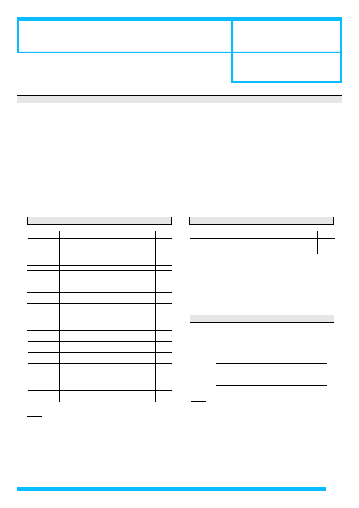
REGISTERS TABLE
Register
40001
40002
40003
40004
40005
40006
40007
40008
40009
40010
40011
40012
40013
40014
40015
40016
40017
40018
40019
40020
40021
40022
40023
40024
40025
40026
40027
40028
40029
40030
NOTE:
The registers marked with ' * ' in the ' E2P ' column are saved in
EEPROM each time they are written, to be automatically reloaded
to each power-on of the device.
Description
Test
Firmware Version
Device Name
Communication
Address
RX/TX Delay
Watchdog Timer
Coils
-- (reserved)
Channel Enable
-- (reserved)
-- (reserved)
Input # 0
Input # 1
Input # 2
Input # 3
-- (reserved)
-- (reserved)
-- (reserved)
-- (reserved)
Sync. value input # 0
Sync. value input # 1
Sync. value input # 2
Sync. value input # 3
-- (reserved)
-- (reserved)
-- (reserved)
-- (reserved)
Access
R/W
R
R
R/W
R/W
R/W
R/W
R/W
R/W
R/W
R/W
R/W
R/W
R
R
R
R
R
R
R
R
R
R
R
R
R
R
R
R
R
E2P
*
*
*
*
*
*
*
*
*
COILS TABLE
Coil
00009
00010
00011
Description
Watchdog Enable
Watchdog Event
Power Up Event
Access
R/W
R/W
R/W
E2P
IMPLEMENTED MODBUS FUNCTIONS
Function
01
02
03
04
05
06
15
16
08
NOTE:
For DAT3000 series devices, the bank 0xxxx is a mirror of bank
1xxxx, as the 3xxxx bank is a mirror of bank 4xxxx, as for i.e. the
first register can be read indifferently as 30001 (with the function
04) or 40001 (with the function 03)
Description
Read multiple coils (0xxxx bank)
Read multiple coils (1xxxx bank)
Read multiple registers (4xxxx bank)
Read multiple registers (3xxxx bank)
Write single coil
Write single register
Write multiple coils
Write multiple registers
Diagnostic
pag 1/4
DESCRIZIONE REGISTRI
40001 : TEST
This register is used to perform the following functions:
- Analog inputs calibration (see the “Procedures” section).
- Synchronized sampling (see the “Procedures” section).
40002 / 40003 : FIRMW ARE VERSION
Read-only 2-register field, that hold the manufacturer firmware identifier.
- Manufacturer default: 3310 (hex)
40004 / 40005 : DEVICE NAME
2-registers field (4 byte or 4 ASCII characters) user free, that can hold the device name or a function identifier. Each byte can be writed with each
value from 0 to 255, than ASCII characters too.
- Manufacturer default: “3015” (ASCII).
40006 : COMMUNICATION
Set the bits of this register as shown in the following table, to set the baud-rate, the bit number, the parity type and the protocol type.
- Manufacturer default:38400 bps, RTU mode
15-14-13-12-11-10-09-08-07-06M05P104P003N02B201B100
Bit
Desc.
Mode
ASCII
Parity
Mark
Even
Odd
Space
NOTES:
- the bit number is ignored, as for in ASCII mode it is fixed to 7 and in RTU mode it is fixed to 8.
- In RTU mode the parity is ignored (parity NONE)
40007 : ADDRESS
Specify the net address of the device; there are allowed the address from 1 to 255.
Each device connected to the same net must have a unique address.
The address 255 is used for broadcast functions (i.e. synchronized sampling)
- Manufacturer default: 01
40008 : RX/TX DELAY
Specify the value of the delay between the reception of a command and the response transmission, indicated in milliseconds.
- Manufacturer default: 1 (1 ms.)
RTU
P1
M
0
1
P0
0
0
0
1
1
0
1
1
B0
BaudRate
1200
2400
4800
9600
19200
38400
---
---
N°bit
7 bit
8 bit
B2
N
0
1
B1
B0
0
0
0
0
0
1
0
1
0
0
1
1
1
0
0
1
0
1
1
1
0
1
1
1
40009 : WATCHDOG TIMER
Specify the value of the W atchDog Timer (see the “Procedures” section), indicated in steps of 0.5 seconds.
- Manufacturer default: 10 (5 sec.)
40010 : COILS
This register is a mirror of the coils table: each bit of this register corresponds to a coil, as shown in the following table.
15-14-13-12-11-10-09-08-07-06-05-04-03-0211011000
Bit
Coil
40011 : (reserved)
This register must have the default value:
DAT3015-V = 04
DAT3015-I = 06
09
pag 2/4
 Loading...