

Datasheet DLV-3.3-6-2.5-7-D48T, DLV-3.3-6-2.5-7-D48S, DLV-3.3-6-2.5-7-D48N, DLV-3.3-6-2.5-7-D48I, DLV-2.5-7-1.8-7-D48T Datasheet (DATEL)
...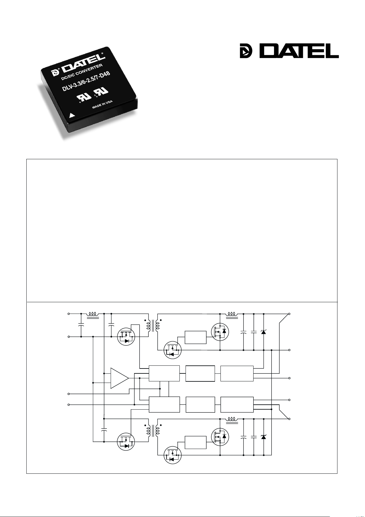
Output Combinations of 3.3V, 2.5V and 1.8V
30 Watt, DC/DC Converters
Dual Output
Mixed Voltage, DLV Models
Features
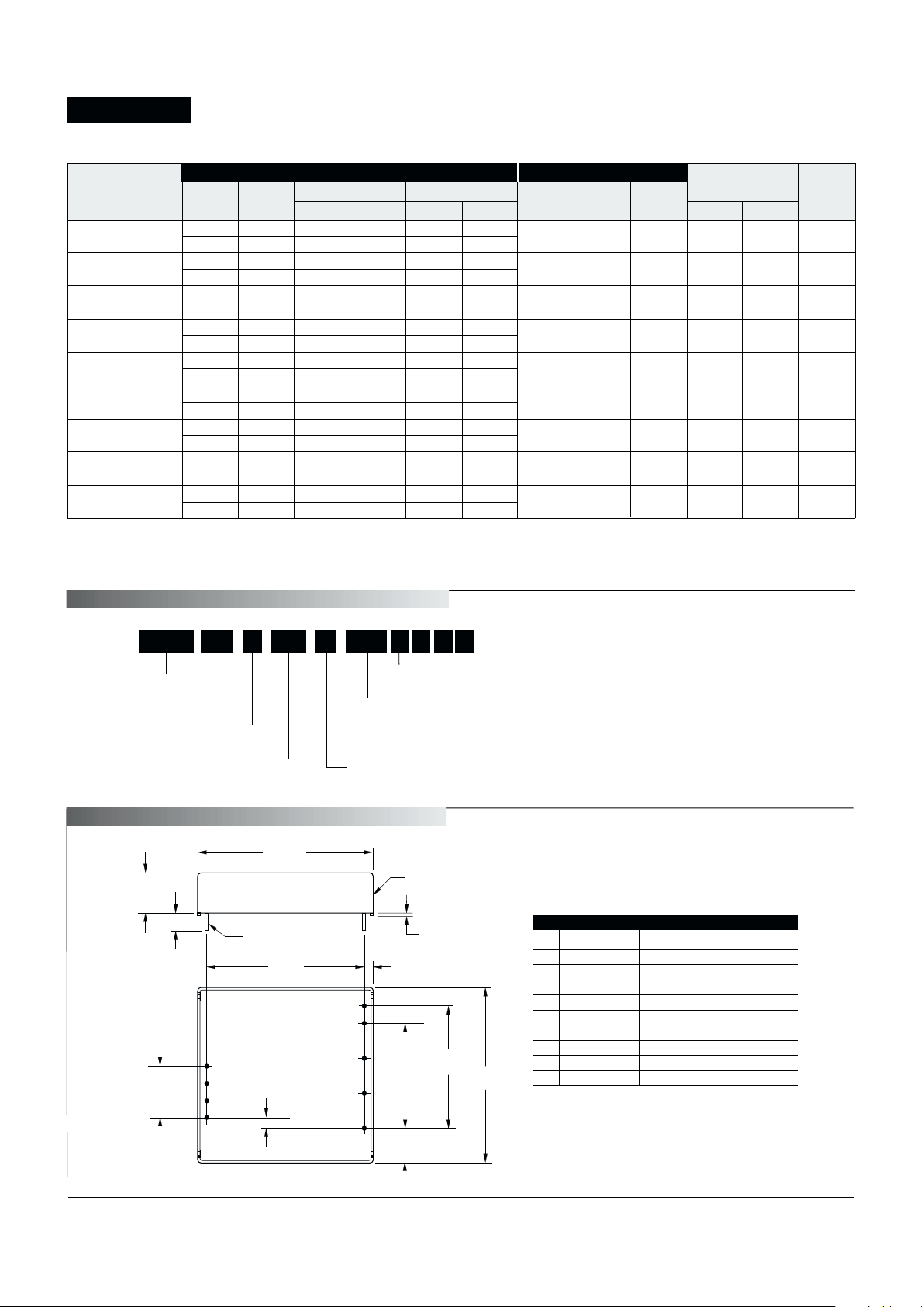
Figure 1. Simplifi ed Schematic
INNOVATION and EX C ELL E N C
E
®
®
■
■
■
■
■
■
■
■
■
■
■
■
■
DATEL, Inc., Mansfi eld, MA 02048 (USA) · Tel: (508)339-3000, (800)233-2765 Fax: (508)339-6356 · Email: sales@datel.com · Internet: www.datel.com
The DLV (Dual Low Voltage) Series from DATEL provides both digital I/O and
core logic supply voltages from a single 2" x 2" industry-standard pinout, plastic
package. The DLV-3.3/6-2.5/7 provides 3.3V @ 6 Amps and 2.5V @ 7 Amps, the
DLV-3.3/6-1.8/7 provides 3.3V @ 6 Amps and 1.8V @ 7 Amps, and the DLV-2.5/7-
2.5/7 provides 2.5V @ 7 Amps and 1.8V @ 7 Amps. All models are available with
input ranges of 10 to 18V (-D12), 18 to 36V (-D24) or 36 to 75V (-D48).
Plug-in compatibility with a number of converters from other leading manufacturers is possible because DATEL offers these 30 Watt converters with the fl exibility
to add/remove the sync (pin 3) and higher-voltage trim (pin 5). Each output is
independently regulated with its own control loop to provide ±1.0% line and load
regulation. Fully synchronous output topology allows no load operation and high
effi ciencies. Models are available with either positive or negative on/off control and
independent output voltage adjustment. "I" suffi x models offer independent, "higher-
voltage" on/off control for proper power sequencing of core and I/O voltages. Both
outputs are internally synchronized to eliminate asynchronous beat frequencies.
All models include input Pi fi ltering, input overvoltage and undervoltage shut-
down circuitry, output overvoltage protection, output short-circuit and current limiting protection and thermal shutdown. These devices meet IEC950, UL1950 and
EN6950 safety standards. CB reports are available on request. "-D48" models are
CE marked (meet LVD requirements).
Two independently regulated outputs:
3.3V @ 6A, 2.5V @ 7A or 1.8V @7A
30 Watts total output power
Available input voltage ranges:
10-18V, 18-36V or 36-75V
Independent output voltage adjustment
Remote On/Off Control and Sync pins
Synchronous rectifi er; No load operation
2" x 2" package; Industry standard pinout
IEC950/UL1950/EN60950 certifi ed
CE mark available (75V
IN models)
Input under and overvoltage shutdown
Output overvoltage protection
Thermal shutdown
Fully Isolated (1500Vdc)
–INPUT
PWM
CONTROLLER
OPTO
ISOLATION
REFERENCE &
ERROR AMP
SWITCH
CONTROL
V2 OUTPUT
SWITCH
CONTROL
OUTPUT
RETURN
V1 OUTPUT
V1 TRIM
(OPTION)
V2 TRIM
+INPUT
SYNC
(OPTION)
ON/OFF
CONTROL
INPUT UNDERVOLTAGE
AND OVERVOLTAGE
COMPARATORS
PWM
CONTROLLER
OPTO
ISOLATION
REFERENCE &
ERROR AMP
PRELIMINARY
30W, DUAL OUTPUT, MIXED-VOLTAGE DC/DC CONVERTERS
DLV Series
PART NUMBER STRUCTURE
V1 Nominal Output Voltage
3.3DLV 6-/ D48-
Input Voltage Range:
D12 = 10-18 Volts (12V nominal)
D24 = 18-36 Volts (24V nominal)
D48 = 36-75 Volts (48V nominal)
I
1 Maximum Output Current
Dual Low Voltage/
Mixed-Voltage Series
2.5 7/- T
V2 Nominal Output Voltage
I
2 Maximum Output Current
Add T, S, N and I suffi xes
as desired
Part Number Suffi xes
Standard DLV DC/DC’s provide a Trim function (Pin 9) for the lower
of the two output voltages. A Trim pin (Pin 5) for the higher voltage can
be added by indicating a "T" suffi x. A Sync pin can also be added and
is indicated by an "S" suffi x. An "N" suffi x indicates that the On/Off
Control function incorporates negative polarity logic. An "I" suffi x provides
independent on/off control (Pin 4) for the higher output voltage.
No Suffi x Pins 3 & 5 not installed, positive polarity On/Off Control
T Suffi x Pin 5 added for higher voltage Trim option
S Suffi x Pin 3 added for Sync Option
N Suffi x Negative polarity On/Off Control
I Suffi x Pin 4 independent on/off control of Pin 6 output voltage
MEC ANICAL SPECIFI CATIONS
2
I/O Connections
Pin Function P40 Function P47 Function P48
1 +Input +Input +Input
2 –Input –Input –Input
3 Sync* Sync* Sync*
4 On/Off Control On/Off Control On/Off Control
5 +3.3V Trim* +3.3V Trim* +2.5V Trim*
6 +3.3V Output +3.3V Output +2.5V Output
7 Output Return Output Return Output Return
8 +2.5V Output +1.8V Output +1.8V Output
9 +2.5V Trim +1.8V Trim +1.8V Trim
Performance Specifi cations and Ordering Guide
➀
DLV-2.5/7-1.8/7-D12
2.5 7 75 TBD ±1% ±1%
12 10-18 TBD TBD 83% C26, P48
1.8 7 75 TBD ±1% ±1%
DLV-2.5/7-1.8/7-D24
2.5 7 75 TBD ±1% ±1%
24 18-36 TBD TBD 83% C26, P48
1.8 7 75 TBD ±1% ±1%
DLV-2.5/7-1.8/7-D48
2.5 7 75 TBD ±1% ±1%
48 36-75 TBD TBD 83% C26, P48
1.8 7 75 TBD ±1% ±1%
DLV-3.3/6-1.8/7-D12
3.3 6 75 TBD ±1% ±1%
12 10-18 TBD TBD 83% C26, P47
1.8 7 75 TBD ±1% ±1%
DLV-3.3/6-1.8/7-D24
3.3 6 75 TBD ±1% ±1%
24 18-36 TBD TBD 83% C26, P47
1.8 7 75 TBD ±1% ±1%
DLV-3.3/6-1.8/7-D48
3.3 6 75 TBD ±1% ±1%
48 36-75 TBD TBD 83% C26, P47
1.8 7 75 TBD ±1% ±1%
DLV-3.3/6-2.5/7-D12
3.3 6 75 TBD ±1% ±1%
12 10-18 TBD TBD 85% C26, P40
2.5 7 75 TBD ±1% ±1%
DLV-3.3/6-2.5/7-D24
3.3 6 75 TBD ±1% ±1%
24 18-36 TBD TBD 85% C26, P40
2.5 7 75 TBD ±1% ±1%
DLV-3.3/6-2.5/7-D48
3.3 6 75 TBD ±1% ±1%
48 36-75 TBD TBD 85% C26, P40
2.5 7 75 TBD ±1% ±1%
➀ Typical at TA = +25°C under nominal line voltage and "balanced," full-power
conditions: 3.3V @ 4.5A/2.5V @ 6A; 3.3V @ 5.2A/1.8V @ 7A; 2.5V @ 7A/1.8V @ 7A.
➁ Any combination of rated I
OUT current, not to exceed 30 Watts of output power.
(See derating graphs.)
Output
Input
R/N (mVp-p) ➂ Regulation (Max.) Effi ciency
Packag e
VOUT IOUT ➁ VIN Nom. Range IIN ➄ (Case,
Model (Volts) (Amps) Typ. Max. Line Load ➃ (Volts) (Volts) (mA) Min. Typ. Pinout)
BOTTOM VIEW
9
8
5
6
7
1
2
3
4
2.00
(50.08)
1.400
(35.56)
1.200
(30.48)
3 EQ. SP. @
0.400 (10.16)
1.800
(45.72)
0.10
(2.54)
0.10
(2.54)
0.40
(10.16)
0.600
(15.24)
3 EQ. SP. @
0.200 (5.08)
PLASTIC CASE
0.040 ±0.001 DIA.
(1.016 ±0.025)
0.20 MIN
(5.08)
2.00
(50.08)
0.48
(12.19)
STANDOFF
0.020 (0.51)
Case C26
* Optional pins
➂ Ripple/Noise (R/N) measured over a 20MHz bandwidth. All models are specicfi ed with
TBD ceramic capacitors.
➃ Tested from no load to 100% load (other output at no load).
➄ Nominal line voltage, no load/balanced full-power condition.
S N I
See page 5 for ordering information.

DLV Models
30W, DUAL OUTPUT, MIXED-VOLTAGE DC/DC CONVERTERS
Performance/Functional Specifi cations
Typical @ TA = +25°C under nominal line voltage, balanced "full-load" conditions, unless noted. ➀
Input
Input Voltage Range:
D12 Models 10-18 Volts (12V nominal)
D24 Models 18-36 Volts (24V nominal)
D48 Models 36-75 Volts (48V nominal)
Overvoltage Shutdown:
D12 Models 19-23 Volts (21V nominal)
D24 Models 37-42 Volts (40V nominal)
D48 Models 77-81 Volts (79V nominal)
Start-Up Threshold:
D12 Models 9-10 Volts (9.3V nominal)
D24 Models 16.5-18 Volts (17V nominal)
D48 Models 34.5-36 Volts (35V nominal)
Undervoltage Shutdown:
D12 Models 8.5-9.6 Volts (9.3V nominal)
D24 Models 16-17 Volts (16.5V nominal)
D48 Models 33-35 Volts (34V nominal)
Input Current:
Normal Operating Conditions See Ordering Guide
Standby Mode:
Off, OV, UV, Thermal Shutdown 10mA typical
Input Refl ected Ripple Current:
Source Impedance
D12 Models TBD
D24 Models TBD
D48 Models TBD
Internal Input Filter Type Pi (0.039µF - 2.2µH - TBD)
Reverse-Polarity Protection:
D12 Models TBD minute duration, 6A maximum
D24 Models TBD minute duration, 4A maximum
D48 Models TBD minute duration, 2A maximum
On/Off Control (Pin 4):
➂ ➃ ➅
D12, D24, D48 Models On = open or TBD to +V
IN,
I
IN = TBDµA @ TBDV
Off = 0-0.8V, I
IN = TBD @ 0V
D12N, D24N, D48N Models On = 0-0.8V, I
IN = TBD @ 0V
Off = open or TBD to +5.5V
I
IN = TBDµA @ TBDV
Sync (Option, Pin 3): ➂ ➃
Input Threshold (Rising Edge Active) 1-2.7 Volts
Input Voltage Low 0-0.9 Volts
Input Voltage High 2.8-5 Volts
Input Resistance 35kΩ minimum
Output High Voltage (100µA load) 3.5-4.8 Volts
Output Drive Current 35mA
Input/Output Pulse Width 160-360nsec
Output
VOUT Accuracy
2.5V/1.8V Models 1.5% / 2% maximum
3.3V/1.8V Models 1% / 2% maximum
3.3V/2.5V Models 1% / 1.5% maximum
Minimum Loading Per Specifi cation No load
Ripple/Noise (20MHz BW) See Ordering Guide
Line/Load Regulation See Ordering Guide
Effi ciency See Ordering Guide/Effi ciency Cur ves
Trim Range
➇ ±5% each output
Isolation Voltage:
Input-to-Output 1500Vdc
Isolation Capacitance 470pF
Isolation Resistance 100MΩ
Output (continued)
Isolation Resistance 100MΩ
Current Limit Inception:
2.5/1.8V Models
2.5V @ 98%V
OUT TBD Amps
1.8V @ 98%V
OUT TBD Amps
3.3/1.8V Models
3.3V @ 98.5%V
OUT TBD Amps
1.8V @ 98%V
OUT TBD Amps
3.3V/2.5V Models
3.3V @ 98.5%V
OUT TBD Amps
2.5V @ 98%V
OUT TBD Amps
Short Circuit Current:
3.3V Outputs TBD Amps average, continuous
2.5V Outputs TBD Amps average, continuous
1.8V Outputs TBD Amps average, continuous
Overvoltage Protection: Comparator, magnetic feedback
2.5/1.8V Models TBD/TBD
3.3/1.8V Models TBD/TBD
3.3/2.5V Models TBD/TBD
Maximum Capacitive Loading
2.5/1.8V Models TBD/TBDµF
3.3/1.8V Models TBD/TBDµF
3.3/2.5V Models TBD/TBDµF
Temperature Coeffi cient ±0.02% per °C
Dynamic Characteristics
Dynamic Load Response:
2.5/1.8V Models
2.5V (50-100% step to 1.5%V
OUT) TBD µsec maximum
1.8V (50-100% step to 2%V
OUT) TBD µsec maximum
3.3/1.8V Models
3.3V (50-100% step to 1%V
OUT) TBD µsec maximum
1.8V (50-100% step to 2%V
OUT) TBD µsec maximum
3.3V/2.5V Models
3.3V (50-100% step to 1%V
OUT) TBD µsec maximum
2.5V (50-100% step to 1.5%V
OUT) TBD µsec maximum
Start-Up Time:
V
IN to VOUT TBD
On/Off to V
OUT TBD
Switching Frequency 225kHz (±TBD kHz)
Environmental
MTBF
D12 Models TBD hours
D24 Models TBD hours
D48 Models TBD hours
Operating Temperature (Ambient):
Without Derating:
2.5/1.8V Models
D12 Model TBD
D24 Model TBD
D48 Model TBD
3.3/1.8V Models
D12 Model TBD
D24 Model TBD
D48 Model TBD
3.3V/2.5V Models
D12 Model TBD
D24 Model TBD
D48 Model TBD
With Derating To +100°C (See Derating Curves)
Case Temperature:
Maximum Operational +100°C
For Thermal Shutdown TBD minimum, TBD maximum
Storage Temperature –40 to +120°C
3

30W, DUAL OUTPUT, MIXED-VOLTAGE DC/DC CONVERTERS
DLV Series
Physical
Dimensions 2" x 2" x 0.5" (50.8 x 50.8 x 12.7mm)
Case Material Diallyl phthalate, UL94V-0 rated
Pin Material Brass, solder coated
Weight: TBD
Primary to Secondary Insulation Level Operational
Absolute Maximum Ratings
Input Voltage:
Continuous: D12 Models 23 Volts
D2A Models 42 Volts
D48 Models 81 Volts
Transient (100msec): D12 Models 25 Volts
D24 Models 50 Volts
D48 Models 100 Volts
Input Reverse-Polarity Protection
➁ Input Current must be limited. TBD
minute duration. Fusing recommended.
D12A Models 6 Amps
D24A Models 4 Amps
D48A Models 2 Amps
Output Current
➁ Current limited. Devices can withstand
an indefi nite output short circuit.
On/Off Control (Pin 4) Max. Voltages
Referenced to –Input (pin 2)
No Suffi x +VIN
"N" Suffi x +8 Volts
Sync Control (Pin 3) Max. Voltages
"S" Suffi x +5.7 Volts
Storage Temperature –40 to +120°C
Lead Temperature (Soldering, 10 sec.) +300°C
These are stress ratings. Exposure of devices to any of these conditions may adversely
affect long-term reliability. Proper operation under conditions other than those listed in the
Performance/Functional Specifi cations Table is not implied, nor recommended.
4
Figure 2. Trim Connections Using A Trim Pot
Figure 3. Trim Connections To Decrease Output Voltages Using Fixed Resistors
➀ All models are specifi ed with external TBD ceramic output capacitors.
➁ See Technical Notes/Graphs for details.
➂ Devices may be order with opposite polarity. Sync pin available with "S" suffi x. See Part
Number Suffi xes and Technical Notes for details.
➃ Applying a voltage to On/Off Control (pin 4) or the Sync (pin 3) when no input power is
applied to the converter may cause permanent damage.
➄ Output noise may be further reduced with the installation of additional external output
capacitors. See Technical Notes.
➅ On/Off control is designed to be driven with open collector or by appropriate voltage
levels. Voltages must be referenced to the –Input (pin 2).
➆ Demonstrated MTBF available on request.
➇ Trim function for the higher of two voltages available with "T" suffi x. See Part
Number Suffi xes and Technical Notes for details.
+3.3V
LOAD
–INPUT
ON/OFF
CONTROL
+INPUT
+3.3V OUTPUT
OUTPUT
RETURN
+2.5V OUTPUT
+2.5V TRIM
7
8
1
4
9
5
6
3
2
+2.5V
LOAD
20kΩ
5-22
TURNS
20kΩ
5-22
TURNS
+3.3V TRIM *
SYNC *
* OPTIONAL PIN
+3.3V
LOAD
–INPUT
ON/OFF
CONTROL
+INPUT
+3.3V OUTPUT
OUTPUT
RETURN
+2.5V OUTPUT
+2.5V TRIM
7
8
1
4
9
5
6
3
2
+2.5V
LOAD
RTRIM DOWN
RTRIM DOWN
+3.3V TRIM *
SYNC *
* OPTIONAL PIN
TECHNICAL NOTES
Trimming Output Voltages
These DLV converters have a trim capability (pins 9 & 5) that allow users
to independently adjust the output voltages ±5%. (Note: pin 5 is an option,
see ordering information.) Adjustments to the output voltages can be accom-
plished via a trim pot, Figure 2, or a single fi xed resistor as shown in Figures
3 and 4. A single fi xed resistor can increase or decrease the output voltage
depending on its connection. Fixed resistors should have absolute TCR's less
than 100ppm/°C to minimize sensitivity to changes in temperature.
A single resistor connected from the Trim pin 9 to +Output (pin 8), see Figure
3, will decrease the lower output voltage. A resistor connected from Trim pin 9
to Output Return (pin 7) will increase the lower output voltage. See Figure 4.
Similarly, the higher output voltage can be adjusted using a single resistor
connected from the Trim (pin 5) to +Output (pin 6) or to Output Return (pin
7). See Figures 3 and 4.
–28.7
DOWN
RT (kΩ) =
3.3 – V
O
3.48(VO – 1.577)
L
N
L
N
–19.7
DOWN
RT (kΩ) =
2.5 – V
O
2.41(VO – 1.18)
L
N
L
N
2.5 Volt Trim Down
–14.17
DOWN
RT (kΩ) =
1.8 – V
O
1.73(VO – 0.86)
L
N
L
N
1.8 Volt Trim Down
3.3 Volt Trim Down

DLV Models
30W, DUAL OUTPUT, MIXED-VOLTAGE DC/DC CONVERTERS
Higher Voltage Control of "Higher" Independent On/Off
Trim Sync Function Positive/Negative Output Voltage Control, Both Outputs
(Pin 5 Installed) (Pin 3 Installed) Logic (Via Pin 4) (Via Pin 4) Suffi x
Positive
No Yes No Suffi x
No
Yes No I
Negative
No Yes N
No
Yes No NI
Positive
No Yes S
Ye s
Yes No SI
Negative
No Yes SN
Yes No SNI
Positive
No Yes T
No
Yes No TI
Negative
No Yes TN
Ye s
Yes No TNI
Positive
No Yes TS
Ye s
Yes No TSI
Negative
No Yes TSN
Yes No TSNI
Ordering Information
DATEL makes no representation that the use of its products in the circuits described herein, or the use of other technical information contained herein, will not infringe upon existing or future patent rights. The descriptions contained herein do
not imply the granting of licenses to make, use, or sell equipment constructed in accordance therewith. Specifi cations are subject to change without notice. The DATEL logo is a registered DATEL, Inc. trademark.
DATEL (UK) LTD. Tadley, England Tel: (01256)-880444
DATEL S.A.R.L. Montigny Le Bretonneux, France Tel: 01-34-60-01-01
DATEL GmbH München, Germany Tel: 89-544334-0
DATEL KK Tokyo, Japan Tel: 3-3779-1031, Osaka Tel: 6-6354-2025
DATEL, Inc. 11 Cabot Boulevard, Mansfi eld, MA 02048-1151
Tel: (508) 339-3000 (800) 233-2765 Fax: (508) 339-6356
Internet: www.datel.com Email: sales@datel.com
ISO 9001 REGISTERED
INNOVATION and EX C ELL E N C
E
®
®
DS-0490 12/00
Figure 4. Trim Connections To Increase Output Voltages Using Fixed Resistors
+3.3V
LOAD
+3.3V TRIM *
–INPUT
SYNC *
ON/OFF
CONTROL
+INPUT
* OPTIONAL PIN
+3.3V OUTPUT
OUTPUT
RETURN
+2.5V OUTPUT
+2.5V TRIM
7
8
1
4
9
5
6
3
2
+2.5V
LOAD
RTRIM UP
RTRIM UP
PART NUMBER STRUCTURE
V1 Nominal Output Voltage
3.3DLV 6-/ D48-
Input Voltage Range:
D12 = 10-18 Volts (12V nominal)
D24 = 18-36 Volts (24V nominal)
D48 = 36-75 Volts (48V nominal)
I
1 Maximum Output Current
Dual Low Voltage/
Mixed-Voltage Series
2.5 7/- T
V2 Nominal Output Voltage
I2 Maximum Output Current
Add T, S, N and I suffi xes
as desired
S N I
Part Number Suffi xes
Standard DLV DC/DC’s provide a Trim function (Pin 9) for the lower
of the two output voltages. A Trim pin (Pin 5) for the higher voltage can
be added by indicating a "T" suffi x. A Sync pin can also be added and
is indicated by an "S" suffi x. An "N" suffi x indicates that the On/Off
Control function incorporates negative polarity logic. An "I" suffi x provides
independent on/off control (Pin 4) for the higher output voltage.
No Suffi x Pins 3 & 5 not installed, positive polarity On/Off Control
T Suffi x Pin 5 added for higher voltage Trim option
S Suffi x Pin 3 added for Sync Option
N Suffi x Negative polarity On/Off Control
I Suffi x Pin 4 independent on/off control of Pin 6 output voltage
Note: Resistor values are in kΩ. Accuracy
of adjustment is subject to
tolerances of resistors and fac-
tory-adjusted output accuracy.
V
O = desired output voltage.
5
–28.7
UP
RT (kΩ) =
V
O – 3.3
5.88
L
N
L
N
–19.7
UP
RT (kΩ) =
V
O – 2.5
2.84
L
N
L
N
2.5 Volt Trim Up
–14.17
UP
RT (kΩ) =
V
O – 1.8
1.49
L
N
L
N
1.8 Volt Trim Up
3.3 Volt Trim Up
 Loading...