DATEL DLV-3.3-6-2.5-7-D48T, DLV-3.3-6-2.5-7-D48S, DLV-3.3-6-2.5-7-D48N, DLV-3.3-6-2.5-7-D48I, DLV-2.5-7-1.8-7-D48T Datasheet
...
Output Combinations of 3.3V, 2.5V and 1.8V
30 Watt, DC/DC Converters
Dual Output
Mixed Voltage, DLV Models
Features
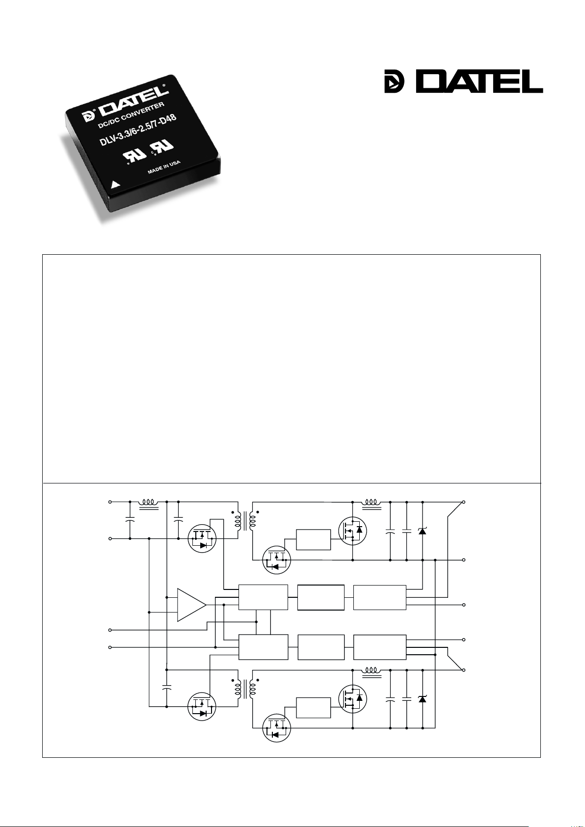
Figure 1. Simplifi ed Schematic
INNOVATION and EX C ELL E N C
E
®
®
■
■
■
■
■
■
■
■
■
■
■
■
■
DATEL, Inc., Mansfi eld, MA 02048 (USA) · Tel: (508)339-3000, (800)233-2765 Fax: (508)339-6356 · Email: sales@datel.com · Internet: www.datel.com
The DLV (Dual Low Voltage) Series from DATEL provides both digital I/O and
core logic supply voltages from a single 2" x 2" industry-standard pinout, plastic
package. The DLV-3.3/6-2.5/7 provides 3.3V @ 6 Amps and 2.5V @ 7 Amps, the
DLV-3.3/6-1.8/7 provides 3.3V @ 6 Amps and 1.8V @ 7 Amps, and the DLV-2.5/7-
2.5/7 provides 2.5V @ 7 Amps and 1.8V @ 7 Amps. All models are available with
input ranges of 10 to 18V (-D12), 18 to 36V (-D24) or 36 to 75V (-D48).
Plug-in compatibility with a number of converters from other leading manufacturers is possible because DATEL offers these 30 Watt converters with the fl exibility
to add/remove the sync (pin 3) and higher-voltage trim (pin 5). Each output is
independently regulated with its own control loop to provide ±1.0% line and load
regulation. Fully synchronous output topology allows no load operation and high
effi ciencies. Models are available with either positive or negative on/off control and
independent output voltage adjustment. "I" suffi x models offer independent, "higher-
voltage" on/off control for proper power sequencing of core and I/O voltages. Both
outputs are internally synchronized to eliminate asynchronous beat frequencies.
All models include input Pi fi ltering, input overvoltage and undervoltage shut-
down circuitry, output overvoltage protection, output short-circuit and current limiting protection and thermal shutdown. These devices meet IEC950, UL1950 and
EN6950 safety standards. CB reports are available on request. "-D48" models are
CE marked (meet LVD requirements).
Two independently regulated outputs:
3.3V @ 6A, 2.5V @ 7A or 1.8V @7A
30 Watts total output power
Available input voltage ranges:
10-18V, 18-36V or 36-75V
Independent output voltage adjustment
Remote On/Off Control and Sync pins
Synchronous rectifi er; No load operation
2" x 2" package; Industry standard pinout
IEC950/UL1950/EN60950 certifi ed
CE mark available (75V
IN models)
Input under and overvoltage shutdown
Output overvoltage protection
Thermal shutdown
Fully Isolated (1500Vdc)
–INPUT
PWM
CONTROLLER
OPTO
ISOLATION
REFERENCE &
ERROR AMP
SWITCH
CONTROL
V2 OUTPUT
SWITCH
CONTROL
OUTPUT
RETURN
V1 OUTPUT
V1 TRIM
(OPTION)
V2 TRIM
+INPUT
SYNC
(OPTION)
ON/OFF
CONTROL
INPUT UNDERVOLTAGE
AND OVERVOLTAGE
COMPARATORS
PWM
CONTROLLER
OPTO
ISOLATION
REFERENCE &
ERROR AMP
PRELIMINARY

30W, DUAL OUTPUT, MIXED-VOLTAGE DC/DC CONVERTERS
DLV Series
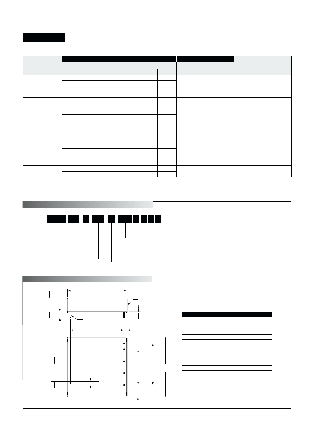
PART NUMBER STRUCTURE
V1 Nominal Output Voltage
3.3DLV 6-/ D48-
Input Voltage Range:
D12 = 10-18 Volts (12V nominal)
D24 = 18-36 Volts (24V nominal)
D48 = 36-75 Volts (48V nominal)
I
1 Maximum Output Current
Dual Low Voltage/
Mixed-Voltage Series
2.5 7/- T
V2 Nominal Output Voltage
I
2 Maximum Output Current
Add T, S, N and I suffi xes
as desired
Part Number Suffi xes
Standard DLV DC/DC’s provide a Trim function (Pin 9) for the lower
of the two output voltages. A Trim pin (Pin 5) for the higher voltage can
be added by indicating a "T" suffi x. A Sync pin can also be added and
is indicated by an "S" suffi x. An "N" suffi x indicates that the On/Off
Control function incorporates negative polarity logic. An "I" suffi x provides
independent on/off control (Pin 4) for the higher output voltage.
No Suffi x Pins 3 & 5 not installed, positive polarity On/Off Control
T Suffi x Pin 5 added for higher voltage Trim option
S Suffi x Pin 3 added for Sync Option
N Suffi x Negative polarity On/Off Control
I Suffi x Pin 4 independent on/off control of Pin 6 output voltage
MEC ANICAL SPECIFI CATIONS
2
I/O Connections
Pin Function P40 Function P47 Function P48
1 +Input +Input +Input
2 –Input –Input –Input
3 Sync* Sync* Sync*
4 On/Off Control On/Off Control On/Off Control
5 +3.3V Trim* +3.3V Trim* +2.5V Trim*
6 +3.3V Output +3.3V Output +2.5V Output
7 Output Return Output Return Output Return
8 +2.5V Output +1.8V Output +1.8V Output
9 +2.5V Trim +1.8V Trim +1.8V Trim
Performance Specifi cations and Ordering Guide
➀
DLV-2.5/7-1.8/7-D12
2.5 7 75 TBD ±1% ±1%
12 10-18 TBD TBD 83% C26, P48
1.8 7 75 TBD ±1% ±1%
DLV-2.5/7-1.8/7-D24
2.5 7 75 TBD ±1% ±1%
24 18-36 TBD TBD 83% C26, P48
1.8 7 75 TBD ±1% ±1%
DLV-2.5/7-1.8/7-D48
2.5 7 75 TBD ±1% ±1%
48 36-75 TBD TBD 83% C26, P48
1.8 7 75 TBD ±1% ±1%
DLV-3.3/6-1.8/7-D12
3.3 6 75 TBD ±1% ±1%
12 10-18 TBD TBD 83% C26, P47
1.8 7 75 TBD ±1% ±1%
DLV-3.3/6-1.8/7-D24
3.3 6 75 TBD ±1% ±1%
24 18-36 TBD TBD 83% C26, P47
1.8 7 75 TBD ±1% ±1%
DLV-3.3/6-1.8/7-D48
3.3 6 75 TBD ±1% ±1%
48 36-75 TBD TBD 83% C26, P47
1.8 7 75 TBD ±1% ±1%
DLV-3.3/6-2.5/7-D12
3.3 6 75 TBD ±1% ±1%
12 10-18 TBD TBD 85% C26, P40
2.5 7 75 TBD ±1% ±1%
DLV-3.3/6-2.5/7-D24
3.3 6 75 TBD ±1% ±1%
24 18-36 TBD TBD 85% C26, P40
2.5 7 75 TBD ±1% ±1%
DLV-3.3/6-2.5/7-D48
3.3 6 75 TBD ±1% ±1%
48 36-75 TBD TBD 85% C26, P40
2.5 7 75 TBD ±1% ±1%
➀ Typical at TA = +25°C under nominal line voltage and "balanced," full-power
conditions: 3.3V @ 4.5A/2.5V @ 6A; 3.3V @ 5.2A/1.8V @ 7A; 2.5V @ 7A/1.8V @ 7A.
➁ Any combination of rated I
OUT current, not to exceed 30 Watts of output power.
(See derating graphs.)
Output
Input
R/N (mVp-p) ➂ Regulation (Max.) Effi ciency
Packag e
VOUT IOUT ➁ VIN Nom. Range IIN ➄ (Case,
Model (Volts) (Amps) Typ. Max. Line Load ➃ (Volts) (Volts) (mA) Min. Typ. Pinout)
BOTTOM VIEW
9
8
5
6
7
1
2
3
4
2.00
(50.08)
1.400
(35.56)
1.200
(30.48)
3 EQ. SP. @
0.400 (10.16)
1.800
(45.72)
0.10
(2.54)
0.10
(2.54)
0.40
(10.16)
0.600
(15.24)
3 EQ. SP. @
0.200 (5.08)
PLASTIC CASE
0.040 ±0.001 DIA.
(1.016 ±0.025)
0.20 MIN
(5.08)
2.00
(50.08)
0.48
(12.19)
STANDOFF
0.020 (0.51)
Case C26
* Optional pins
➂ Ripple/Noise (R/N) measured over a 20MHz bandwidth. All models are specicfi ed with
TBD ceramic capacitors.
➃ Tested from no load to 100% load (other output at no load).
➄ Nominal line voltage, no load/balanced full-power condition.
S N I
See page 5 for ordering information.
 Loading...