

DATEL CDS1402MM, CDS1402MC Datasheet
1 OFFSET ADJUST V1
2 DO NOT CONNECT
3 ANALOG INPUT 1
4 ANALOG INPUT 2
5 ANALOG GROUND
6 S/H1 OUT
7 S/H1 ROUT
8 S/H2 SUMMING NODE
9 OFFSET ADJUST V2
10 DO NOT CONNECT
11 S/H1 COMMAND
12 S/H2 COMMAND
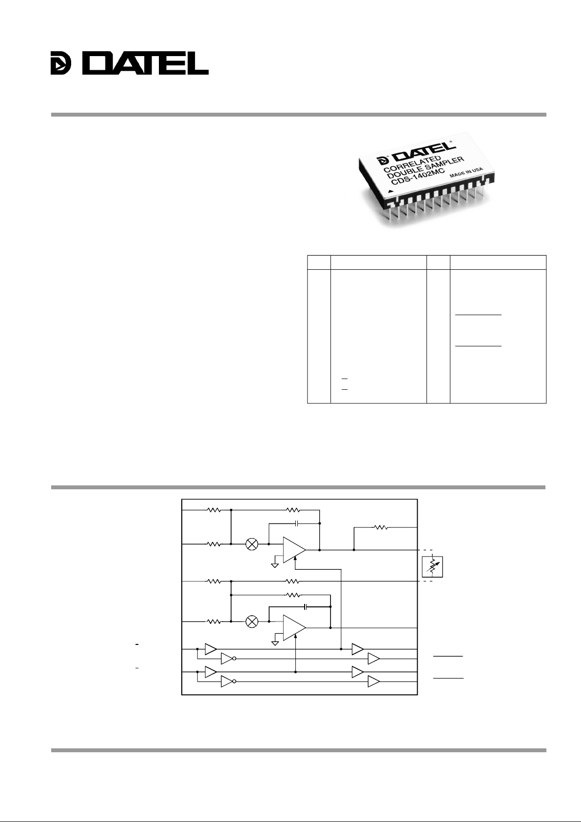
INPUT/OUTPUT CONNECTIONS
24 +5V ANALOG SUPPLY
23 ANALOG GROUND
22 V OUT
21 ANALOG GROUND
20 A/D CLOCK2
19 A/D CLOCK2
18 A/D CLOCK1
17 A/D CLOCK1
16 +5V DIGITAL SUPPLY
15 DIGITAL GROUND
14 ANALOG GROUND
13 –5V ANALOG SUPPLY
FEATURES
• Use with 10 to 14-bit A/D converters
• 5 Megapixels/second minimum throughput (14 bits)
• ±2.5V input/output ranges, Gain = –1
• Low noise, 200µVrms
• Two independent S/H amplifiers
• Gain matching between S/H's
• Offset adjustments for each S/H
• Four external A/D control lines
• Small package, 24-pin ceramic DDIP
• Low power, 350mW
• Low cost
GENERAL DESCRIPTION
The CDS-1402 is an application-specific, correlated double
sampling (CDS) circuit designed for electronic-imaging
applications that employ CCD’s (charge coupled devices) as
their photodetector. The CDS-1402 has been optimized for
use in digital video applications that employ 10 to 14-bit A/D
converters. The low-noise CDS-1402 can accurately
determine each pixel’s true video signal level by sequentially
sampling the pixel’s offset signal and its video signal and
subtracting the two. The result is that the consequences of
residual charge, charge injection and low-frequency “kTC”
noise on the CCD’s output floating capacitor are effectively
eliminated. The CDS-1402 can also be used as a dual
sample-hold amplifier in a data acquisition system.
The CDS-1402 contains two sample-hold amplifiers and
appropriate support/control circuitry. Features include
independent offset-adjust capability for each S/H, adjustment
for matching gain between the two S/H’s, and four control
PIN FUNCTION PIN FUNCTION
INNOVATION and EX C ELL E N C E
® ®
CDS-1402
14-Bit, Faster-Settling
Correlated Double Sampling Circuit
Figure 1. CDS-1402 Functional Block Diagram
lines for triggering the A/D converter used in conjunction with
the CDS-1402. The CDS circuit’s “ping-pong” timing
approach (the offset signal of the “n+1” pixel can be acquired
while the video output of the “nth” pixel is being converted)
guarantees a minimum throughput, in a 14-bit application, of
5MHz. In other words, the true video signal (minus offset)
will be available
(continued on page 4-13)
S/H 2
OFFSET ADJUST V1 1
DO NOT CONNECT 2
ANALOG INPUT 1 3
OFFSET ADJUST V2 9
DO NOT CONNECT 10
ANALOG INPUT 2 4
S/H1 COMMAND 11
S/H2 COMMAND 12
5, 14, 21, 23
ANALOG GROUND24+5V ANALOG
SUPPLY
16
+5V DIGITAL
SUPPLY
15
DIGITAL
GROUND
7 S/H1 ROUT
8 S/H2
SUMMING NODE
22 V OUT
18 A/D CLOCK 1
6 S/H1 OUT
OPTIONAL
17 A/D CLOCK 1
19 A/D CLOCK 2
20 A/D CLOCK 2
100k
Ω
100k
Ω
450
Ω
500
Ω
13
–5V ANALOG
SUPPLY
–
+
S/H 1
–
+
500
Ω
500
Ω
500
Ω
50
Ω
CH
CH
DATEL, Inc., 11 Cabot Boulevard, Mansfield, MA 02048-1151 (U.S.A.) • Tel: (508) 339-3000 Fax: (508) 339-6356 • For immediate assistance (800) 233-2765
2
CDS-1402
® ®
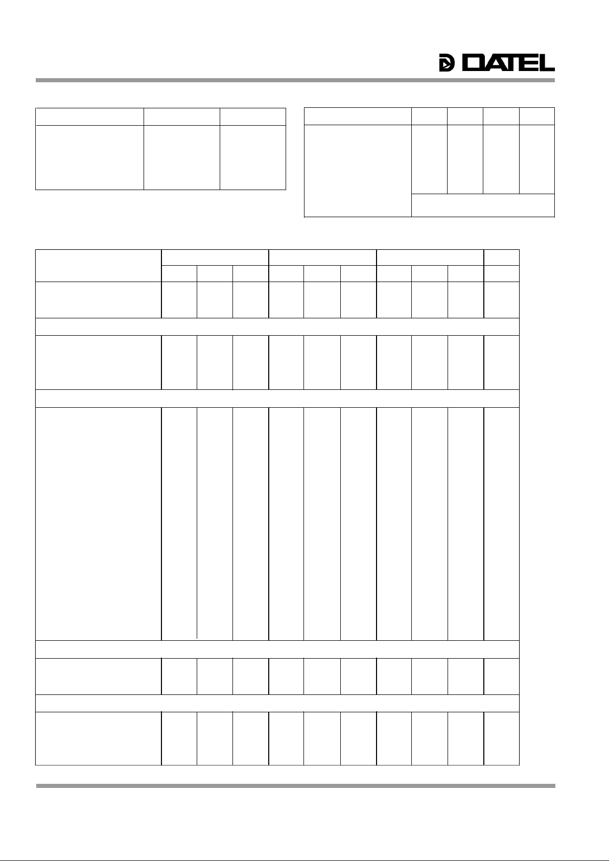
+25°C 0 to +70°C –55 to +125°C
ANALOG INPUTS ➀ MIN. TYP. MAX. MIN. TYP. MAX. MIN. TYP. MAX. UNITS
Input Voltage Range ±2.5 — — ±2.5 — — ±2.5 — — Volts
Input Resistance — 500 — — 500 — — 500 — Ohms
Input Capacitance — 7 15 — 7 15 — 7 15 pF
DIGITAL INPUTS
Logic Levels
Logic "1" +2.0 — — +2.0 — — +2.0 — — Volts
Logic "0" — — +0.8 — — +0.8 — — +0.8 Volts
Logic Loading "1" — — +10 — — +10 — — +10 µA
Logic Loading "0" — — –10 — — –10 — — –10 µA
PERFORMANCE
Sample Mode Offset Error - S/H1 — ±3 — — ±4 — — ±5 — mV
Gain Error - S/H1 — ±0.1 — — ±0.2 — — ±0.4 — %
Pedestal - S/H1 — ±10 — — ±10 — — ±15 — mV
Sample Mode Offset Error - S/H2 — ±3 — — ±4 — — ±5 — mV
Gain Error - S/H2 — ±0.1 — — ±0.2 — — ±0.4 — %
Pedestal - S/H2 — ±10 — — ±10 — — ±15 — mV
Sample Mode Offset Error - CDS — ±1 — — ±4 — — ±5 — mV
Differential Gain Error - CDS — ±0.1 — — ±0.2 — — ±0.4 — %
Pedestal - CDS — ±10 — — ±10 — — ±15 — mV
Pixel Rate (14-bit settling) ➁ 5 — — 5 — — 5 — — MHz
Input Bandwidth, ±2.5V
Small Signal (–20dB input) — TBD — — TBD — — TBD — MHz
Large Signal (–0.5dB input) — TBD — — TBD — — TBD — MHz
Slew Rate — ±500 — — ±500 — — ±500 — V/µs
Aperture Delay Time — 10 — — 10 — — 10 — ns
Aperture Uncertainty — 5 — — 5 — — 5 — ps rms
S/H Acquisition Time ➀
(to ±0.01%, 5V step) — 100 — — 100 — — 100 — ns
Hold Mode Settling Time
(to ±0.15mV) — TBD — — TBD — — TBD — ns
Noise — 200 — — 200 — — 200 — µVrms
Feedthrough Rejection — TBD — — TBD — — TBD — dB
Overvoltage Recovery Time — 200 — — 200 — — 200 — ns
S/H Saturation Voltage — ±3.2 — — ±3.2 — — ±3.2 — V
Droop Rate — ±5 — — ±10 — — ±25 — mV/µs
ANALOG OUTPUTS ➂
Output Voltage Range ±2.5 — — ±2.5 — — ±2.5 — — Volts
Output Impedance — 0.5 — — 0.5 — — 0.5 — Ohms
Output Current — — ±20 — — ±20 — — ±20 mA
DIGITAL OUTPUTS
Logic Levels
Logic "1" +3.9 — — +3.9 — — +3.9 — — Volts
Logic "0" — — +0.4 — — +0.4 — — +0.4 Volts
Logic Loading "1" — — –4 — — –4 — — –4 mA
Logic Loading "0" — — +4 — — +4 — — +4 mA
PARAMETERS LIMITS UNITS
+5V Analog Supply (Pin 24) 0 to +6.3 Volts
–5V Analog Supply (Pin 13) 0 to –6.3 Volts
+5V Digital Supply (Pin 16) 0 to +6 Volts
Digital Inputs (Pins 11, 12) –0.3 to +V
DD +0.3 Volts
Analog Inputs (Pins 3, 4) ±3.2 Volts
Lead Temperature (10 seconds) 300 °C
ABSOLUTE MAXIMUM RATINGS
➀ Pins 3 and 4. ➁ See Figure 5 for relationship between input voltage, accuracy, and acquisition time. ➂ Pins 6 and 22.
FUNCTIONAL SPECIFICATIONS
(TA = +25°C, ±VCC = ±5V, +VDD = +5V, pixel rate = 5MHz, and a minimum warmup time of two minutes unless otherwise noted.)
PARAMETERS MIN. TYP. MAX. UNITS
Operating Temp. Range, Case
CDS-1402MC 0 — +70 °C
CDS-1402MM –55 — +125 °C
Thermal Impedance
θjc — 5 — °C/W
θca — 22 — °C/W
Storage Temperature Range –65 — +150 °C
Package Type 24-pin, metal-sealed, ceramic DDIP
Weight 0.42 ounces(12 grams)
PHYSICAL/ENVIRONMENTAL

3
® ®
CDS-1402
+25°C 0 to +70°C –55 to +125°C
POWER REQUIREMENTS MIN. TYP. MAX. MIN. TYP. MAX. MIN. TYP. MAX. UNITS
Power Supply Ranges
+5V Analog Supply +4.75 +5.0 +5.25 +4.75 +5.0 +5.25 +4.75 +5.0 +5.25 Volts
–5V Analog Supply –4.75 –5.0 –5.25 –4.75 –5.0 –5.25 –4.75 –5.0 –5.25 Volts
+5V Digital Supply +4.75 +5.0 +5.25 +4.75 +5.0 +5.25 +4.75 +5.0 +5.25 Volts
Power Supply Currents
+5V Analog Supply — +35 +45 — +35 +45 — +35 +45 mA
–5V Analog Supply — –35 –45 — –35 –45 — –35 –45 mA
+5V Digital Supply — +2 +5 — +2 +5 — +2 +5 mA
Power Dissipation — 350 450 — 350 450 — 350 450 mW
Power Supply Rejection — 60 — — 60 — — 60 — dB
GENERAL DESCRIPTION (continued)
at the output of the CDS-1402 every 200ns. This correlates
with the fact that an acquisition time of 100ns is required for
each internal S/H amplifier (5V step acquired to ±0.003%
accuracy). The input and output of the CDS-1402 can swing
up to ±2.5 Volts.
The functionally complete CDS-1402 is packaged in a single,
24-pin, ceramic DDIP. It operates from ±5V analog and +5V
digital supplies and consumes 350mW. Though the CDS1402’s approach to CDS appears straightforward (see
Description of Operation), the circuit actually exploits an
elegant architecture whose tradeoffs enable it to offer widebandwidth, low-noise and high-throughput combinations
unachievable until now. The CDS-1402, a generic type of
circuit, can be used with most 10 to 14-bit A/D converters.
However, DATEL offers A/D converters optimized for use with
CDS-1402.
FUNCTIONAL DESCRIPTION
Correlated Double Sampling
All photodetector elements (photodiodes, photomultiplier tubes,
focal plane arrays, charge coupled devices, etc.) have unique
output characteristics that call for specific analog-signalprocessing (ASP) functions at their outputs. Charge coupled
devices (CCD’s), in particular, display a number of unique
characteristics. Among them is the fact that the “offset error”
associated with each individual pixel (i.e., the apparent
photonic content of that pixel after having had no light incident
upon it) changes each and every time that particular pixel is
accessed.
Most of us think of an offset as a constant parameter that
either can be compensated for (by performing an offset
adjustment) or can be measured, recorded, and subtracted
from subsequent readings to yield more accurate data.
Contending with an offset that varies from reading to reading
requires measuring and recording (or capturing and storing)
the offset each and every time, so it can be subtracted from
each subsequent data reading.
The “double sampling” aspect of CDS refers to the operation of
sampling and storing/recording a given pixel’s offset and then
sampling the same pixel’s output an instant later (with both the
offset and the video signal present) and subsequently
subtracting the two values to yield what is referred to as the
“valid video” output for that pixel.
The “correlated” in CDS refers to the fact that the two samples
must be taken close together in time because the offset is
constantly varying. Reasons for this phenomena are
discussed below.
At the output of all CCD’s, transported pixel charge (electrons)
is converted to a voltage by depositing the charge onto a
capacitor (usually called the output or “floating” capacitor).
The voltage that develops across this capacitor is obviously
proportional to the amount of deposited charge (i.e., the
number of electrons) according to ∆V = ∆Q/C. Once settled,
the resulting capacitor voltage is buffered and brought to the
CCD’s output pin as a signal whose amplitude is proportional
to the total number of photons incident upon the relevant pixel.
After the output signal has been recorded, the floating
capacitor is discharged (“reset”, “clamped”, “dumped”) and
made ready to accept charge from the next pixel. This is
when the problems begin. (This is a somewhat oversimplified
TECHNICAL NOTES
1. To achieve specified performance, all popwer supply pins
should be bypassed with 2.2µF tantalum capacitors in
parallel with 0.01µF ceramic capacitors. All ANALOG
GROUND (pins 5, 14, 21 and 23) and DIGITAL GROUND
(pin 15) pins should be tied to a large analog ground plane
beneath the package.
2. In the CDS configuration, to avoid saturation of the S/H
amplifiers, the maximum analog inputs and conditions are
as follows:
ANALOG INPUT 1 < ±3.2V
(ANALOG INPUT 1 – ANALOG INPUT 2) < ±3.2V
3. The combined video and reference/offset signal from the
CCD array must be applied to S/H2, while the reference/
offset signal is applied to S/H1.
4. To use as a CDS circuit, tie pin 8 (S/H2 SUMMING NODE)
to either pin 6 (S/H1 OUT), through a 100 Ohm
potentiometer, or directly to pin 7 (S/H1 ROUT). In both
cases, the CCD's output is tied to pins 3 (ANALOG INPUT
1) and 4 (ANALOG INPUT 2). As shown in Figure 5, the
100Ω potentiometer is for gain matching.
5. To use as a dual S/H, leave pin 7 (S/H1 ROUT) and pin 8
(S/H2 SUMMING NODE) floating. Pin 6 (S/H1 OUT) will
be the output of S/H1 and pin 22 (V OUT) will be the output
of S/H2.
6. See Figure 4 for acquisition time versus accuracy and input
voltage step amplitude.
 Loading...