

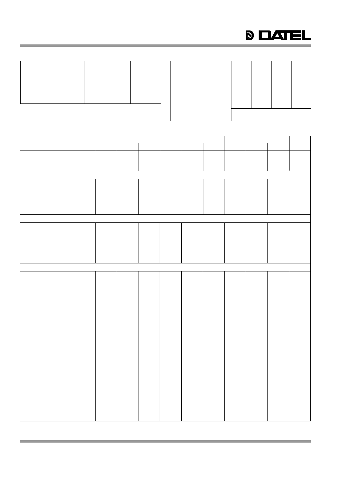
Figure 1. ADS-947 Functional Block Diagram
FEA TURES
••
••
• 14-bit resolution
••
••
• 10MHz minimum sampling rate
••
••
• No missing codes over full military temperature range
••
••
• Ideal for both time and frequency-domain applications
••
••
• Excellent THD (–81dB) and SNR (76dB)
••
••
• Edge-triggered
••
••
• Small, 24-pin, ceramic DDIP or SMT
••
••
• Requires only +5V and –5.2V supplies
••
••
• Low-power, 2 Watts
••
••
• Low cost
GENERAL DESCRIPTION
The low-cost ADS-947 is a 14-bit, 10MHz sampling A/D
converter. This device accurately samples full-scale input
signals up to Nyquist frequencies with no missing codes.
Excellent differential nonlinearity error (DNL), signal-to-noise
ratio (SNR), and total harmonic distortion (THD) make the
ADS-947 the ideal choice for both time-domain (CCD/FPA
imaging, scanners, process control) and frequency-domain
(radar, telecommunications, spectrum analysis) applications.
The functionally complete ADS-947 contains a fast-settling
sample/hold amplifier, a subranging (two-pass) A/D converter,
an internal reference, timing/control logic, and error-correction
circuitry. Digital input and output levels are TTL. The ADS-947
only requires the rising edge of a start convert pulse to
operate.
Requiring only +5V and –5.2V supplies, the ADS-947 typically
dissipates just 2 Watts. The device is offered with a bipolar
input range of ±2V. Models are available for use in either
commercial (0 to +70°C) or military (–55 to +125°C) operating
®®
temperature ranges. A proprietary, auto-calibrating, errorcorrecting circuit allows the device to achieve specified
performance over the full military temperature range.
INPUT/OUTPUT CONNECTIONS
PRELIMINARY PRODUCT DATA
REF
DAC
REGISTER
REGISTER
OUTPUT REGISTER
16 BIT 14 (LSB)
15 BIT 13
12 BIT 12
11 BIT 11
10 BIT 10
9 BIT 9
8 BIT 8
7 BIT 7
6 BIT 6
5 BIT 5
4 BIT 4
3 BIT 3
2 BIT 2
1 BIT 1 (MSB)
TIMING AND
CONTROL LOGIC
OFFSET ADJUST 23
ANALOG INPUT 21
START CONVERT 18
DATA VALID 17
+5V ANALOG SUPPLY 22
+5V DIGITAL SUPPLY 13
–5.2V SUPPLY 20
ANALOG GROUND 19, 24
DIGITAL GROUND 14
–
+
S/H
BUFFER
DIGITAL CORRECTION LOGIC
FLASH
ADC
1
FLASH
ADC
2
POWER AND GROUNDING
S
AMP
PIN FUNCTION PIN FUNCTION
1 BIT 1 (MSB) 24 ANALOG GROUND
2 BIT 2 23 OFFSET ADJUST
3 BIT 3 22 +5V ANALOG SUPPLY
4 BIT 4 21 ANALOG INPUT
5 BIT 5 20 –5.2V SUPPLY
6 BIT 6 19 ANALOG GROUND
7 BIT 7 18 START CONVERT
8 BIT 8 17 DATA VALID
9 BIT 9 16 BIT 14 (LSB)
10 BIT 10 15 BIT 13
11 BIT 11 14 DIGITAL GROUND
12 BIT 12 13 +5V DIGITAL SUPPLY
ADS-947
14-Bit, 10MHz
Sampling A/D Converters
DATEL, Inc., Mansfield, MA 02048 (USA) • Tel: (508) 339-3000, (800) 233-2765 Fax: (508) 339-6356 • Email: sales@datel.com • Internet: www.datel.com
ADS-947
2
®®
+25°C 0 to +70°C –55 to +125°C
ANALOG INPUT MIN. TYP. MAX. MIN. TYP. MAX. MIN. TYP. MAX. UNITS
Input Voltage Range ➁ — ±2 — — ±2 — — ±2 — Volts
Input Resistance — 250 — — 250 — — 250 — Ω
Input Capacitance — 6 15 — 6 15 — 6 15 pF
DIGITAL INPUT
Logic Levels
Logic "1" +2.0 — — +2.0 — — +2.0 — — Volts
Logic "0" — — +0.8 — — +0.8 — — +0.8 Volts
Logic Loading "1" — — +20 — — +20 — — +20 µA
Logic Loading "0" — — –20 — — –20 — — –20 µA
Start Convert Positive Pulse Width ➂ 10 20 — 10 20 — 10 20 — ns
STATIC PERFORMANCE
Resolution — 14 — — 1 4 — — 14 — Bits
Integral Nonlinearity (fin = 10kHz) — ±0.75 — — ±0.75 — — ±1 — LSB
Differential Nonlinearity (fin = 10kHz) –0.95 ±0.5 +1.25 –0.95 ±0.5 +1.25 –0.95 ±0.5 +1.5 LSB
Full Scale Absolute Accuracy — ±0.15 ±0.4 — ±0.15 ±0.4 — ±0.4 ±0.8 %FSR
Bipolar Zero Error (Tech Note 2) — ±0.1 ±0.3 — ±0.1 ±0.3 — ±0.3 ±0.6 %FSR
Gain Error (Tech Note 2) — ±0.2 ±0.4 — ±0.2 ±0.4 — ±0.4 ±1.5 %
No Missing Codes (fin = 10kHz) 14 — — 14 — — 14 — — Bits
DYNAMIC PERFORMANCE
Peak Harmonics (–0.5dB)
dc to 1MHz — –83 –76 — –83 –75 — –79 –71 dB
1MHz to 2.5MHz — –78 –72 — –78 –72 — –73 –68 dB
2.5MHz to 5MHz — –76 –71 — –76 –71 — –71 –65 dB
Total Harmonic Distortion (–0.5dB)
dc to 1MHz — –81 –74 — –81 –74 — –77 –70 dB
1MHz to 2.5MHz — –76 –71 — –76 –71 — –72 –66 dB
2.5MHz to 5MHz — –74 –69 — –74 –69 — –69 –63 dB
Signal-to-Noise Ratio
(w/o distortion, –0.5dB)
dc to 1MHz 72 76 — 72 76 — 70 75 — dB
1MHz to 2.5MHz 72 76 — 72 76 — 70 75 — dB
2.5MHz to 5MHz 71 75 — 71 75 — 70 75 — dB
Signal-to-Noise Ratio ➃
(& distortion, –0.5dB)
dc to 1MHz 70 74 — 70 74 — 68 73 — dB
1MHz to 2.5MHz 70 74 — 70 74 — 66 71 — dB
2.5MHz to 5MHz 68 73 — 68 73 — 65 70 — dB
Noise — 150 — — 150 — — 150 — µVrms
Two-tone Intermodulation
Distortion (fin = 2.45MHz,
1.975MHz, fs = 10MHz, –0.5dB) — –82 — — –82 — — –82 — dB
Input Bandwidth (–3dB)
Small Signal (–20dB input) — 30 — — 30 — — 30 — MHz
Large Signal (–0.5dB input) — 10 — — 10 — — 10 — MHz
Feedthrough Rejection (fin = 5MHz) — 85 — — 85 — — 85 — dB
Slew Rate — ±400 — — ±400 — — ±400 — V/µs
Aperture Delay Time —+5——+5— —+5—ns
Aperture Uncertainty — 2 — — 2 — — 2 — ps rms
FUNCTIONAL SPECIFICATIONS
(TA = +25°C, +VDD = +5V, –VDD = –5.2V, 10MHz sampling rate, and a minimum 3 minute warmup ➀ unless otherwise specified.)
P ARAMETERS MIN. TYP . MAX. UNITS
Operating Temp. Range, Case
ADS-947MC, GC 0 — +70 °C
ADS-947MM, GM, 883 –55 — +125 °C
Thermal Impedance
θjc — 6 — °C/Watt
θca — 23 — °C/Watt
Storage Temperature Range –65 — +150 °C
Package Type 24-pin, metal-sealed, ceramic DDIP or SMT
Weight 0.46 ounces (13 grams)
ABSOLUTE MAXIMUM RATINGS
PARAMETERS LIMITS UNITS
+5V Supply (Pins 13, 22) 0 to +6 Volts
–5.2V Supply (Pin 20) 0 to –5.5V Volts
Digital Input (Pin 18) –0.3 to +VDD +0.3 Volts
Analog Input (Pin 21) ±5 Volts
Lead Temperature (10 seconds) +300 °C
PHYSICAL/ENVIRONMENTAL
ADS-947
3
®®
+25°C 0 to +70°C –55 to +125°C
DYNAMIC PERFORMANCE (Cont.) MIN. TYP. MAX. MIN. TYP. MAX. MIN. TYP. MAX. UNITS
S/H Acquisition Time
( to ±0.003%FSR, 4V step) — 40 45 — 40 45 — 40 45 ns
Overvoltage Recovery Time ➄ — — 100 — — 100 — — 100 ns
A/D Conversion Rate 10 — — 10 — — 10 — — MHz
DIGITAL OUTPUTS
Logic Levels
Logic "1" +2.4 — — +2.4 — — +2.4 — — Volts
Logic "0" — — +0.4 — — +0.4 — — +0.4 Volts
Logic Loading "1" — — –4 — — –4 — — –4 mA
Logic Loading "0" — — +4 — — +4 — — +4 mA
Output Coding
Offset Binary
POWER REQUIREMENTS
Power Supply Ranges ➅
+5V Supply +4.75 +5.0 +5.25 +4.75 +5.0 +5.25 +4.9 +5.0 +5.25 Volts
–5.2V Supply –4.75 –5.2 –5.45 –4.75 –5.2 –5.45 –4.9 –5.2 –5.45 Volts
Power Supply Currents
+5V Supply — +250 +260 — +250 +260 — +250 +260 mA
–5.2V Supply — –200 –210 — –200 –210 — –200 –210 mA
Power Dissipation — 2.0 2.25 — 2.0 2.25 — 2.0 2.25 Watts
Power Supply Rejection — — ±0.1 — — ±0.1 — — ±0.1 %FSR/%V
Footnotes:
TECHNICAL NOTES
1. Obtaining fully specified performance from the ADS-947
requires careful attention to pc card layout and power
supply decoupling. The device’s analog and digital ground
systems are connected to each other internally. For optimal
performance, tie all ground pins (14, 19 and 24) directly to a
large analog ground plane beneath the package.
Bypass all power supplies to ground with 4.7µF tantalum
capacitors in parallel with 0.1µF ceramic capacitors. Locate
the bypass capacitors as close to the unit as possible.
2. The ADS-947 achieves its specified accuracies without the
need for external calibration. If required, the device’s small
initial offset and gain errors can be reduced to zero using
the adjustment circuitry shown in Figures 2 and 3.
When using this circuitry, or any similar offset and gain
calibration hardware, make adjustments f ollowing warmup.
To avoid interaction, always adjust offset before gain.
3. Applying a start convert pulse while a conversion is in
progress (EOC = logic 1) will initiate a new and inaccurate
conversion cycle. Data for the interrupted and subsequent
conversions will be invalid.
4. A passive bandpass filter is used at the input of the A/D for
all production testing.
Figure 2. Optional ADS-947 Gain Adjust Calibration Circuit
➀ All power supplies should be on before applying a start convert pulse. All
supplies and the clock (start convert pulses) must be present during warmup
periods. The device must be continuously converting during this time.
➁ Contact DATEL for other input voltage ranges.
➂ A 10MHz clock with a 20ns positive pulse width is used for all production
testing. See Timing Diagram, figure 4, for more details.
To Pin 21
of ADS-947
–5V
SIGNAL
INPUT
GAIN
ADJUST
1.98k
Ω
50
Ω
+5V
2k
Ω
➄ This is the time required before the A/D output data is valid once the analog
input is back within the specified range. This time is only guaranteed if the
input does not exceed ±2.2V (S/H saturation voltage).
➅ The minimum supply voltages of +4.9V and –5.1V for ±VDD are required for
–55°C operation only. The minimum limits are +4.75V and –4.95V when
operating at +125°C
➃ Effective bits is equal to:
(SNR + Distortion) – 1.76 + 20 log
Full Scale Amplitude
Actual Input Amplitude
6.02

ADS-947
4
®®
CALIBRATION PROCEDURE
Any offset and/or gain calibration procedures should not be
implemented until devices are fully warmed up. To avoid
interaction, offset must be adjusted before gain. The ranges of
adjustment for the circuits in Figures 2 and 3 are guaranteed to
compensate for the ADS-947’s initial accuracy errors and may
not be able to compensate for additional system errors.
A/D converters are calibrated by positioning their digital outputs
exactly on the transition point between two adjacent digital
output codes. This can be accomplished by connecting LED’s
to the digital outputs and adjusting until certain LED’s “flicker”
equally between on and off. Other approaches employ digital
comparators or microcontrollers to detect when the outputs
change from one code to the next.
Offset adjusting for the ADS-947 is normally accomplished at
the point where the MSB is a 1 and all other output bits are 0’s
and the LSB just changes from a 0 to a 1. This digital output
transition ideally occurs when the applied analog input is
+½ LSB (+122µV).
Gain adjusting is accomplished when all bits are 1’s and the
LSB just changes from a 1 to a 0. This transition ideally occurs
when the analog input is at +full scale minus 1½ LSB's
(+1.99963V).
Zero/Offset Adjust Procedure
1. Apply a train of pulses to the START CONVERT input (pin
18) so the converter is continuously converting.
2. Apply +122µV to the ANALOG INPUT (pin 21).
3. Adjust the offset potentiometer until the output bits are
10 0000 0000 0000 and the LSB flickers between 0 and 1.
Gain Adjust Procedure
1. Apply +1.99963V to the ANALOG INPUT (pin 21).
2. Adjust the gain potentiometer until all output bits are 1’s and
the LSB flickers between 1 and 0.
3. To confirm proper operation of the device, vary the input
signal to obtain the output coding listed in Table 2.
BIPOLAR INPUT V OL T A GE OFFSET BINAR Y
SCALE (±2V RANGE) MSB LSB
+FS –1 LSB +1.99976 11 1111 1111 1111
+3/4 FS +1.50000 11 1000 0000 0000
+1/2 FS +1.00000 11 0000 0000 0000
0 0.00000 10 0000 0000 0000
–1/2 FS –1.00000 01 0000 0000 0000
–3/4 FS –1.50000 00 1000 0000 0000
–FS +1 LSB –1.99976 00 0000 0000 0001
–FS –2.00000 00 0000 0000 0000
Table 2. Output Coding for Bipolar Operation
INPUT VOLTAGE ZERO ADJUST GAIN ADJUST
RANGE +½ LSB +FS –1½ LSB
±2V +122µV +1.99963V
Table 1. Gain and Zero Adjust
Figure 3. T ypical ADS-947 Connection Dia gram
0.1µF0.1µF
4.7µF 4.7µF
22, 13
24
2019
ADS-947
–5.2V
20k
W
0.1µF
4.7µF
+5V
14
–5V
+5V
21
23
18
1
2
3
4
5
6
7
8
9
10
11
12
15
16
17
BIT 1 (MSB)
BIT 2
BIT 3
BIT 4
BIT 5
BIT 6
BIT 7
BIT 8
BIT 9
BIT 10
BIT 11
BIT 12
BIT 13
BIT 14 (LSB)
DATA VALID
ANALOG
INPUT
START
CONVERT
A single +5V supply should be used for both the +5V analog and +5V digital.
If separate supplies are used, the difference between the two cannot exceed 100mV.
➀
➀
+ + +
ZERO/
OFFSET
ADJUST

ADS-947
5
®®
Electrically-insulating, thermally-conductive "pads" may be
installed underneath the package. Devices should be soldered
to boards rather than socketed, and of course, minimal air flow
over the surface can greatly help reduce the package
temperature.
In more severe ambient conditions, the package/junction
temperature of a given device can be reduced dramatically
(typically 35%) by using one of DATEL's HS Series heat sinks.
See Ordering Information for the assigned part number. See
page 1-183 of the DATEL Data Acquisition Components Catalog
for more information on the HS Series. Request DATEL
Application Note AN8, "Heat Sinks for DIP Data Converters",
or contact DATEL directly, for additional information.
THERMAL REQUIREMENTS
All DATEL sampling A/D converters are fully character ized
and specified over operating temperature (case) ranges of
0 to +70°C and –55 to +125°C. All room temperature
(T
A = +25°C) production testing is performed without the use
of heat sinks or forced air cooling. Thermal impedance
figures for each device are listed in their respective
specification tables.
These devices do not normally require heat sinks, however,
standard precautionary design and layout procedures should
be used to ensure devices do not overheat. The ground and
power planes beneath the package, as well as all pcb signal
runs to and from the device, should be as heavy as possible
to help conduct heat away from the package.
Figure 4. ADS-947 Timing Diagram
START
CONVERT
OUTPUT
DATA
INTERNAL S/H
NN+1
DATA N-1 VALID
50ns typ.
(±5ns)
20ns
typ.
Acquisition Time
35ns
typ.
Hold
65ns typ.
10ns typ.
DATA N VALID
INVALID DATA
50ns typ.
Notes:
1. Scale is approximately 5ns per division. Sampling rate = 10MHz.
2. The start convert pulse must be between 20 and 50ns wide or between 80 and 100ns wide (when sampling at 10MHz)
to ensure proper operation. For sampling rates less than 10MHz, the start pulse can be wider than 85nsec, however a minimum
pulse width low of 15nsec should be maintained. A 10MHz clock with a 20nsec positive pulse width is used for all production testing.
INTERNAL EOC
25ns typ.
Conversion Time
70ns typ.
DATA N-1 VALID
DATA N VALID
DATA
VALID
40ns typ.
(±5ns)
40ns typ.
(±5ns)
40ns max.
15ns
(61ns min., 68ns max.)
(22ns min., 28ns max.)

ADS-947
6
®®
Figure 5. FFT Analysis of ADS-947
(fs = 8MHz, fin = 3.85MHz, Vin = –0.5dB, 16,384 point FFT)
Figure 6. ADS-947 Histogram and Differential Nonlinearity

ADS-947
7
®®
Figure 7. ADS-947 Evaluation Board Sc hematic (ADS-B947)
GND
Q
CLR
CKDPR
+5VF
+5VA
+15V
–15V
-15V
+15V
–5VA
+5V
–5V
+5VF
–15V
–5VA
OPTION
+5VF
Q
PRDCK
CLR
+5VF
+5VF
+5VF
+5V
–5.2V
+5VA
BIT12
BIT11
BIT10
BIT9
BIT8
BIT7
BIT6
BIT5
BIT4
BIT3
BIT2
BIT1
ADS-947
+5VD
DGND
BIT13
BIT14
DATA VALID
START
AGND
–5.2V
AIN
+5VA
OFFSET
AGND
Q1Q2Q3Q4Q5Q6Q7
Q8
8D7D6D5D4D3D2D
1D
+
+
+
+
+
+
+
–
+5VA+15V
+
+
+
+
+
C15
U6
P2
SG10
SG3
SG2
SG1
C14
C7
C13
C6
C12C5
L7
L6
R1
C20
C4 C11
L5
L4
L3
C3
C10
C2
C9
L2
C8C1
L1
P4
C19
SG8SG7
U4
R2
C18
SG5
SG6
SG4
R3
C26 C27
C25
SG9
C24
C23
C16
C22
C17
C21
X1
U6
P3
JPR1
U5
P1
JPR2
U5
U1
U3
OFFSET
ADJUST
ANA. IN
IN
ANA.
CLC402
HI2541
ANA. IN
START CONVERT
7
8
14
CONVERT
START
74HCT86
B14
B13
B12
B11
B10
B9B8B7B6B5B4B3
B2
B1
TRIG
74HCT86
74HCT573
74HCT573
74HCT86
HCT7474
20k
20µH
HCT7474
10MHz
CRYSTAL
15pF
3.2k
2.2µF
4
5
6
13
12
14
11
7
9
8
131112
10
262422
25232119171513
11
97531
2018161412
10
864
2
2
5
4
11
10
14
5
6
423
1
7
2
31
2
1
3
33
31
34
32302826242220
1816141210
8
6
4
2
29
27
25
23
211917
15
13
11
9
7
5
3
1
2
3
1
9
10
8
123456789
101112
2423222120191817161514
13
10
1
12131415161718
19
20
2345678
9
11
SPARE GATES
C1 - C7 ARE 20V.
2. CLOSE SG1-SG3, SG9, SG10.
ALL RESISTORS ARE IN OHMS.
1. UNLESS OTHERWISE SPECIFIED ALL CAPACITORS ARE 50V.
NOTES:
OE
CE
Q1Q2Q3Q4Q5Q6Q7
Q8
8D7D6D5D4D3D2D
1D
U2
10
12131415161718
19
20
2345678
9
11
OE
CE
1
CE
0.1µF
0.1µF
0.1µF
0.1µF
0.1µF
2.2µF
0.1µF
2.2µF
2.2µF
0.1µF
2.2µF
2.2µF
2.2µF
2.2µF
2.2µF
2.2µF
2.2µF
6
+5VF
(Optional)
(Optional)
(Optional)
(Optional)
0.01µF
0.01µF
0.01µF
0.01µF
0.01µF
0.01µF
0.01µF
0.1µF
U5
U5
20µH
20µH
20µH
20µH
20µH
20µH
Q

ADS-947
®
®
INNOV A TION and EX CELLENCE
DATEL makes no representation that the use of its products in the circuits described herein, or the use of other technical information contained herein, will not infringe upon existing or future patent rights. The descriptions contained herein
do not imply the granting of licenses to make, use, or sell equipment constructed in accordance therewith. Specifications are subject to change without notice. The D ATEL logo is a registered DATEL, Inc. trademark.
DS-0346 01/97
OPERATING 24-PIN
MODEL TEMP . RANGE PA CKAGE
ADS-947MC 0 to +70°C DDIP
ADS-947MM –55 to +125°C DDIP
ADS-947/883 –55 to +125°C DDIP
ADS-947GC 0 to +70°C SMT
ADS-947GM –55 to +125°C SMT
MECHANICAL DIMENSIONS INCHES (mm)
24-Pin DDIP
Versions
ADS-947MC
ADS-947MM
0.200 MAX.
(5.080)
0.235 MAX.
(5.969)
0.600 ±0.010
(15.240)
0.80 MAX.
(20.32)
0.100 TYP.
(2.540)
0.100
(2.540)
0.018 ±0.002
(0.457)
0.100
(2.540)
0.040
(1.016)
1.31 MAX.
(33.27)
112
13
24
1.100
(27.940)
0.190 MAX.
(4.826)
0.010
(0.254)
+0.002
–0.001
SEATING
PLANE
0.025
(0.635)
Dimension Tolerances
(unless otherwise indicated):
2 place decimal (.XX) ±0.010 (±0.254)
3 place decimal (.XXX) ±0.005 (±0.127)
Lead Material:
Kovar alloy
Lead Finish:
50 microinches (minimum) gold plating
over 100 microinches (nominal) nickel plating
PIN 1 INDEX
ORDERING INFORMATION
ACCESSORIES
ADS-B947 Evaluation Board (without ADS-947)
HS-24 Heat Sink for all ADS-947 DDIP models
24-Pin
Surface Mount
Versions
ADS-947GC
ADS-947GM
Receptacles for PC board mounting can be ordered through AMP, Inc., Part # 3-331272-8 (Component Lead
Socket), 24 required. For MIL-STD-883 product specifcation, contact DATEL.
®®
ISO 9001
I
SO 9001
REGISTERED
0.80 MAX.
(20.32)
0.015
(0.381)
MAX. radius
for any pin
1.31 MAX.
(33.02)
0.100 TYP.
(2.540)
0.100
(2.540)
0.190 MAX.
(4.826)
0.040
(1.016)
0.020 TYP.
(0.508)
0.020
(0.508)
24
13
121
PIN 1
INDEX
0.130 TYP.
(3.302)
Dimension Tolerances
(unless otherwise indicated):
2 place decimal (.XX) ±0.010 (±0.254)
3 place decimal (.XXX) ±0.005 (±0.127)
Lead Material:
Kovar alloy
Lead Finish:
50 microinches (minimum) gold plating
over 100 microinches (nominal) nickel plating
0.060 TYP.
(1.524)
0.010 TYP.
(0.254)
DATEL, Inc. 11 Cabot Boulevard, Mansfield, MA 02048-1151
Tel: (508) 339-3000 (800) 233-2765 Fax: (508) 339-6356
Internet: www.datel.com Email: sales@datel.com
Data Sheet Fax Back: (508) 261-2857
DATEL (UK) LTD. Tadley, England Tel: (01256)-880444
DATEL S.A.R.L. Montigny Le Bretonneux, France Tel: 01-34-60-01-01
DATEL GmbH München, Germany Tel: 89-544334-0
DATEL KK Tokyo, Japan Tel: 3-3779-1031, Osaka Tel: 6-354-2025
 Loading...