DATEL ADS-EVAL4, ADS-941ME, ADS-941MC Datasheet

® ®
REGISTERREGISTER
START CONVERT 32
DIGITAL CORRECTION LOGIC
GROUND
GROUND
SUPPLY
3-STATE OUTPUT REGISTER
SUPPLY
GROUND
SELECT
SUPPLY
FEATURES
• 14-bit resolution
• 1MHz minimum sampling rate
• Functionally complete
• Internal reference and sample/hold
• No missing codes
• Excellent performance
• Full Nyquist-rate sampling
• Small 32–pin DIP
• Low power, 2.8 Watts
ADS-941
14-Bit, 1MHz
Sampling A/D Converters
GENERAL DESCRIPTION
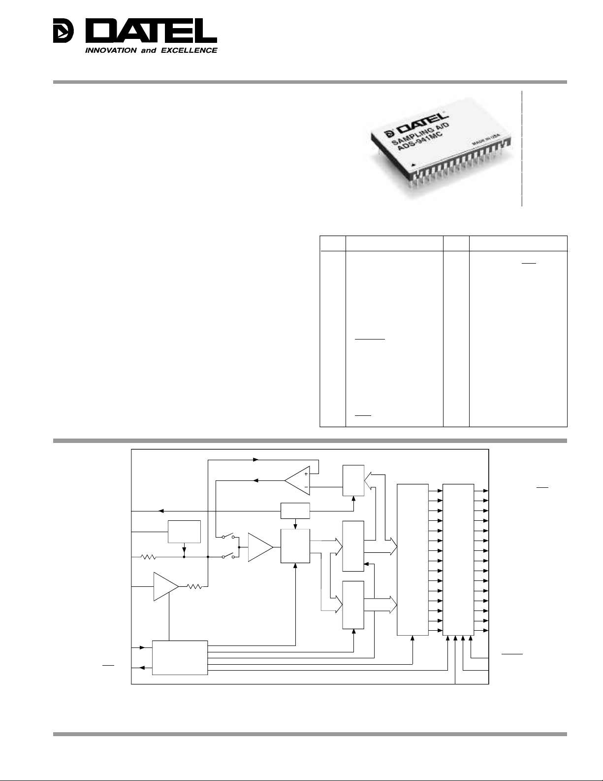
DATEL's ADS-941 is a functionally complete, 14-bit, 1MHz,
sampling A/D converter. Its standard, 32-pin, triple-wide
ceramic DIP contains a fast-settling sample/hold amplifier, a
14-bit subranging (two-pass) A/D converter, a precision
reference, a three-state output register, and all the timing and
control logic necessary to operate from a single start convert
pulse.
The ADS-941 is optimized for wideband frequency-domain
applications and is fully FFT tested. Total harmonic distortion
(THD) and signal-to-noise ratio (including distortion) typically
run at –85dB and 80dB, respectively, with full-scale inputs up
to 100kHz.
The ADS-941 requires ±15V and +5V supplies and typically
consumes 2.8 Watts.
+10V REF. OUT 1
OFFSET ADJUST 5
BIPOLAR 2
ANALOG INPUT 3
S/H
OFFSET
CIRCUIT
S2
S1
BUFFER
REF
FLASH
ADC
INPUT/OUTPUT CONNECTIONS
PIN FUNCTION PIN FUNCTION
1 +10V REF. OUT 32 START CONVERT
2 BIPOLAR 31 BIT 1 OUT (MSB)
3 ANALOG INPUT 30 BIT 1 OUT (MSB)
4 SIGNAL GROUND 29 BIT 2 OUT
5 OFFSET ADJUST 28 BIT 3 OUT
6 ANALOG GROUND 27 BIT 4 OUT
7 OVERFLOW 26 BIT 5 OUT
8 CODING SELECT 25 BIT 6 OUT
9 ENABLE 24 BIT 7 OUT
10 +5V SUPPLY 23 BIT 8 OUT
11 DIGITAL GROUND 22 BIT 9 OUT
12 +15V SUPPLY 21 BIT 10 OUT
13 –15V SUPPLY 20 BIT 11 OUT
14 ANALOG GROUND 19 BIT 12 OUT
15 ANALOG GROUND 18 BIT 13 OUT
16 EOC 17 BIT 14 OUT (LSB)
DAC
31 BIT 1 OUT (MSB)
30 BIT 1 OUT (MSB)
29 BIT 2 OUT
28 BIT 3 OUT
27 BIT 4 OUT
26 BIT 5 OUT
25 BIT 6 OUT
24 BIT 7 OUT
23 BIT 8 OUT
22 BIT 9 OUT
21 BIT 10 OUT
20 BIT 11 OUT
19 BIT 12 OUT
18 BIT 13 OUT
17 BIT 14 OUT (LSB)
EOC 16
TIMING AND
CONTROL LOGIC
4
SIGNAL
10
+5V
11
DIGITAL
12
+15V
6, 14, 15
ANALOG
13
–5V
8
CODING
9 ENABLE
7 OVERFLOW
Figure 1. ADS-941 Functional Block Diagram
DATEL, Inc., 11 Cabot Boulevard, Mansfield, MA 02048-1151 (U.S.A.) • Tel: (508) 339-3000 Fax: (508) 339-6356 • For immediate assistance: (800) 233-2765

ADS-941
® ®
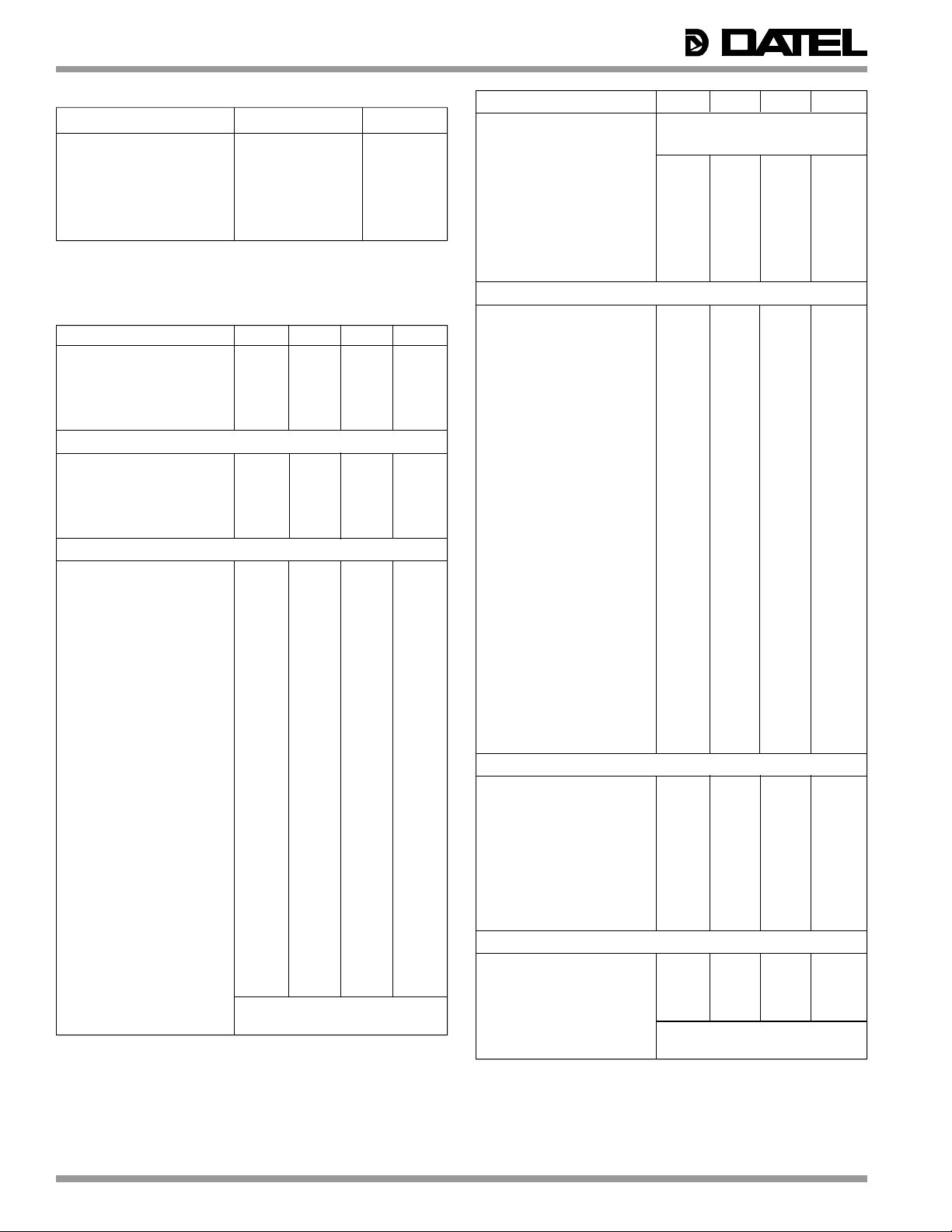
ABSOLUTE MAXIMUM RATINGS
PARAMETERS LIMITS UNITS
+15V Supply (Pin 12) 0 to +16 Volts
–15V Supply (Pin 13) 0 to –16 Volts
+5V Supply (Pin 10) 0 to +6.0 Volts
Digital Inputs (Pin 8,9, 32) –0.3 to +V
DD +0.3 Volts
Analog Input (Pin 3) ±15 Volts
Lead Temp. (10 seconds) 300 °C
FUNCTIONAL SPECIFICATIONS
(TA = +25°C, ±VCC = ±15V, ±VDD = ±5V, 1MHz sampling rate, and a minimum 7 minute
warmup unless otherwise specified.)
ANALOG INPUTS MIN. TYP. MAX. UNITS
Input Voltage Range
Unipolar — 0 to +10 — Volts
Bipolar — ±5 — Volts
Input Impedence 2.2 2.5 — kΩ
Input Capacitance — 7 15 pF
DIGITAL INPUTS
Logic Levels
Logic "1" +2.0 — — Volts
Logic "0" — — +0.8 Volts
Logic Loading "1" — — +10 µA
Logic Loading "0" — — –600 µA
PERFORMANCE
Integral Non-Linearity
in = 10KHz)
(f
+25°C — ±1 ±2 LSB
0 to +70°C — ±1.5 ±2 LSB
–40 to +85°C — ±2 ±3 LSB
Differential Non-Linearity
in = 10KHz)
(f
+25°C –0.75 ±0.5 ±0.75 LSB
0 to +70°C –0.95 ±0.75 ±0.95 LSB
–40 to +85°C –1 ±0.95 +2.5 LSB
Full Scale Absolute Accuracy
+25°C — ±0.1 ±0.122 %FSR
0 to +70°C — ±0.12 ±0.36 %FSR
–40 to +85°C — ±0.45 ±0.85 %FSR
Unipolar Zero Error
+25°C (see Figure 3) — ±0.05 ±0.122 %FSR
0 to +70°C — ±0.1 ±0.2 %FSR
–40 to +85°C — ±0.2 ±0.3 %FSR
Bipolar Zero Error
+25°C (see Figure 3) — ±0.05 ±0.122 %FSR
0 to +70°C — ±0.1 ±0.2 %FSR
–40 to +85°C — ±0.2 ±0.3 %FSR
Bipolar Offset Error
+25°C (see Figure 3) — ±0.1 ±0.12 %FSR
0 to +70°C — ±0.12 ±0.3 %FSR
–40 to +85°C — ±0.6 ±0.8 %FSR
Gain Error
+25°C (see Figure 3) — ±0.018 ±0.122 %
0 to +70°C — ±0.12 ±0.3 %
–40 to +85°C — ±0.6 ±0.8 %
No Missing Codes (f
14 Bits 0 to +70°C
Resolution 14 Bits
in = 500kHz)
OUTPUTS MIN. TYP. MAX. UNITS
Output Coding Staight Bin./Offset Bin./Two's Comp.
Comp. Bin./Comp. Offset Bin./C2C
Logic Level
Logic "1" +2.4 — — Volts
Logic "0" — — +0.4 Volts
Logic Loading "1" — — –160 µA
Logic Loading "0" — — +6.4 mA
Internal Reference
Voltage, +25°C +9.98 +10.0 +10.02 Volts
Drift — ±13 ±30 ppm/°C
External Current — — 5 mA
DYNAMIC PERFORMANCE
Slew Rate — ±250 1 V/µs
Aperature Delay Time — — 10 ns
Aperature Uncertainty — — ±5 ps
S/H Aquisition TIme
(to ±0.003%FS, 10V step) — 250 350 ns
Total Harm. Distort. (–0.5dB)
dc to 100kHz –78 –85 — dB
100kHz to 500kHz –77 –80 — dB
Signal-to-Noise Ratio
(w/o distortion, –0.5dB
dc to 100kHz 75 80 — dB
100kHz to 500kHz 74 77 — dB
Signal-to-Noise Ratio
(and distortion, –0.5dB)
dc to 100kHz 74 80 — dB
100kHz to 500kHz 73 78 — dB
Spurious Free Dyn. Range ➀
dc to 100kHz78 78 86 — dB
100 to 500kHz 77 83 — dB
Two-tone IMD
Distortion (f
in = 100kHz,
240kHz, fs = 2.0Mhz,
–0.5dB) — –85 — dB
Input Bandwidth (–3dB)
Small Signal (–20dB input) — 6 — MHz
Large Signal (–0dB input) — 1.75 — MHz
Feedthrough Rejection
in = 500KHz) — 87 — dB
(f
Overvoltage Recovery, ±12V — 1000 2000 ns
A/D Conversion Rate 1 — — MHz
Noise — 250 — µVrms
POWER REQUIREMENTS
Power Supply Ranges
+15V Supply +14.25 +15.0 +15.75 Volts
–15V Supply –14.25 –15.0 –15.75 Volts
+5V Supply +4.75 +5.0 +5.25 Volts
Power Supply Currents
+15V Supply — +62 +85 mA
–15V Supply — –80 –95 mA
+5V Supply — +140 +160 mA
Power Dissipation — 2.8 3.3 Watts
Power Supply Rejection — — ±0.02 %FSR%V
PHYSICAL/ENVIRONMENTAL
Operating Temp. Range, Case
ADS-941MC 0 — +70 °C
ADS-941ME –40 — +85 °C
Storage Temperature Range –65 — +150 °C
Package Type 32-pin, metal-sealed, ceramic TDIP
Weight 0.46 ounces (13 grams)
Footnote:
➀ Same specification as In-Band Harmonics and Peak Harmonics.
2
 Loading...