


INTEGRATED CIRCUITS
DATA SH EET
TJA1050
High speed CAN transceiver
Preliminary specification
Supersedes data of 1999 Sep 27
File under Integrated Circuits, IC18
2000 May 26

Philips Semiconductors Preliminary specification
High speed CAN transceiver TJA1050
FEATURES
• Fully compatible with the
“ISO 11898”
standard
• High speed (up to 1 Mbaud)
• Very low ElectroMagnetic Emission (EME)
• Differential receiver with wide common-mode range for
high ElectroMagnetic Immunity (EMI)
• An unpowered node does not disturb the bus lines
• Transmit Data (TXD) dominant time-out function
• Silent mode in which the transmitter is disabled
• Bus pins protected against transients in an automotive
environment
GENERAL DESCRIPTION
The TJA1050 isthe interface between the Controller Area
Network (CAN) protocol controller and the physical bus.
The device provides differential transmit capability to the
bus and differential receive capability to the CAN
controller.
The TJA1050 is the successor to the PCA82C250
high-speed CAN transceiver. The most important
improvements are:
• Much lower electromagnetic emission due to optimal
matching of the output signals CANH and CANL
• Improved behaviour in case of an unpowered node.
• Input levels compatible with 3.3 V devices
• Thermally protected
• Short-circuit proof to supply voltage and ground
• At least 110 nodes can be connected.
QUICK REFERENCE DATA
SYMBOL PARAMETER CONDITIONS MIN. MAX. UNIT
V
CC
V
CANH
V
CANL
V
i(dif)(bus)
t
PD(TXD-RXD)
T
amb
supply voltage 4.75 5.25 V
DC voltage at pin CANH 0 < VCC< 5.25 V; no time limit −27 +40 V
DC voltage at pin CANL 0 < VCC< 5.25 V; no time limit −27 +40 V
differential bus input voltage dominant 1.5 3 V
propagation delay TXD to RXD VS= 0 V; see Fig.7 − 250 ns
ambient temperature −40 +125 °C
ORDERING INFORMATION
TYPE
NUMBER
NAME DESCRIPTION VERSION
PACKAGE
TJA1050T SO8 plastic small outline package; 8 leads; body width 3.9 mm SOT96-1
TJA1050U − bare die; die dimensions 1700 x 1280 x 380 µm −
2000 May 26 2
Philips Semiconductors Preliminary specification
High speed CAN transceiver TJA1050
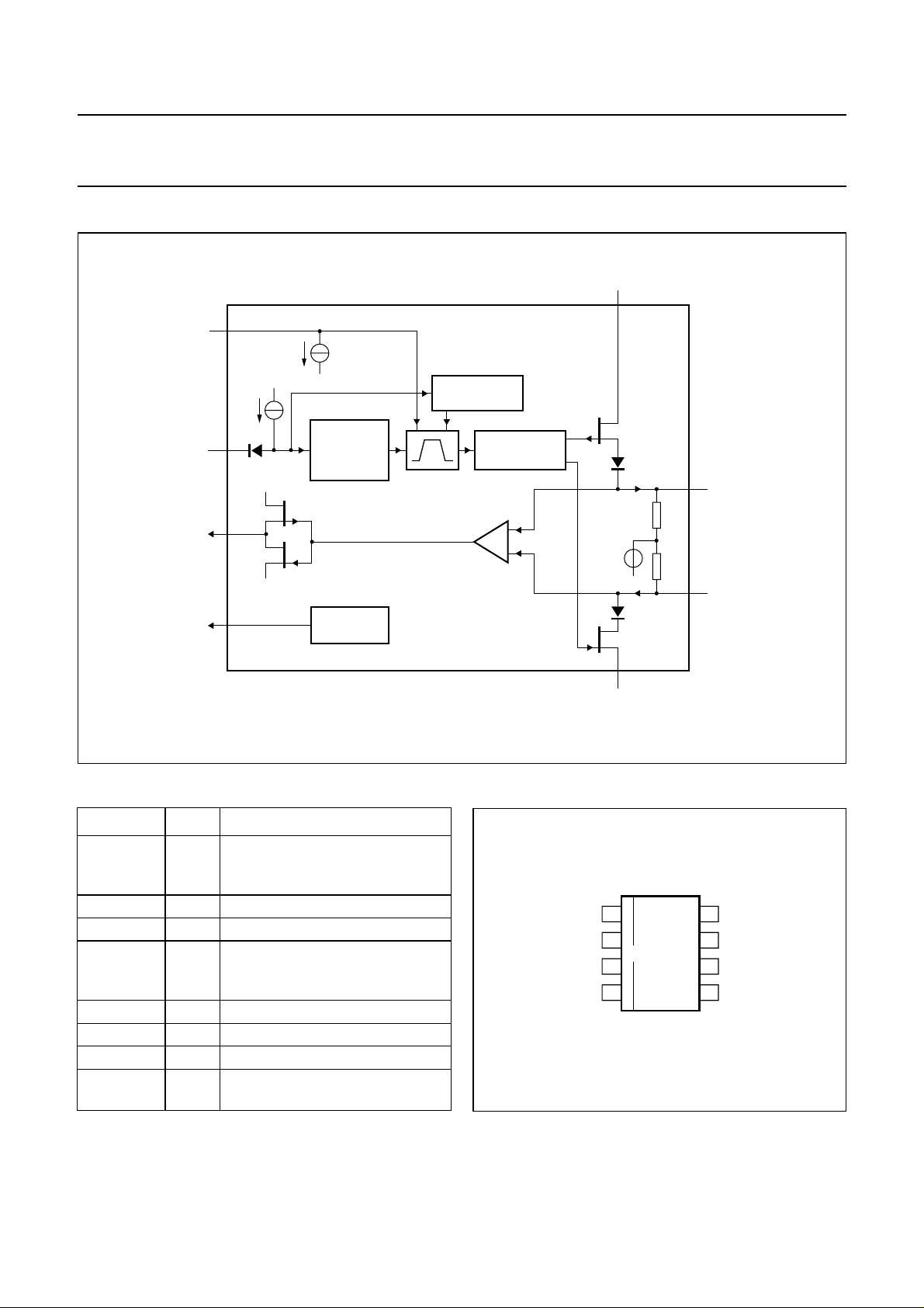
BLOCK DIAGRAM
handbook, full pagewidth
TXD
RXD
V
ref
V
CC
0.5V
CC
GND
3
GND
2
7
25
kΩ
25
kΩ
6
MGS374
CANH
CANL
8
S
30 µA
V
CC
1
4
5
200
µA
V
CC
GND
GND
TXD
DOMINANT
TIME-OUT
TIMER
REFERENCE
VOLTAGE
TEMPERATURE
PROTECTION
DRIVER
RECEIVER
TJA1050
Fig.1 Block diagram.
PINNING
SYMBOL PIN DESCRIPTION
TXD 1 transmit data input; reads in data
from the CAN controller to the bus
line drivers
GND 2 ground
V
CC
3 supply voltage
RXD 4 receive data output; reads out
data from the bus lines to the
CAN controller
V
ref
5 reference voltage output
CANL 6 LOW-level CAN bus line
CANH 7 HIGH-level CAN bus line
S 8 select input for high-speed mode
or silent mode
handbook, halfpage
TXD
1
2
TJA1050T
3
V
CC
4
RXD
MGS375
Fig.2 Pin configuration.
S
8
CANHGND
7
CANL
6
V
5
ref
2000 May 26 3

Philips Semiconductors Preliminary specification
High speed CAN transceiver TJA1050
FUNCTIONAL DESCRIPTION
The TJA1050 is the interface between the CAN protocol
controller and the physical bus. It is primarily intended for
high-speed automotive applicationsusing baud rates from
60 kbaud up to 1 Mbaud. It provides differential transmit
capability to the bus and differential receiver capability to
the CAN protocol controller. It is fully compatible to the
“ISO 11898”
standard.
A current-limiting circuit protects the transmitter output
stage from damage caused by accidental short-circuit to
either positive or negative supply voltage, although power
dissipation increases during this fault condition.
A thermal protection circuit protects the IC from damage
by switching off the transmitter if the junction temperature
exceeds a value of approximately 165 °C. Because the
transmitter dissipates most of the power, the power
dissipation and temperature of the IC is reduced. All other
IC functions continue to operate. The transmitter off-state
resets when pin TXD goes HIGH. The thermal protection
circuit is particularly needed when a bus line short-circuits.
The pins CANH and CANL are protected from automotive
electrical transients (according to
“ISO 7637”
; see Fig.4).
Control pin S allows two operating modes to be selected:
high-speed mode or silent mode.
Thehigh-speed mode isthe normal operating modeand is
selected by connecting pin S to ground. It is the default
mode if pin S is not connected.
In the silent mode, the transmitter is disabled. All other
IC functions continue to operate. The silent mode is
selected by connecting pin S to VCC and can be used to
prevent network communication from being blocked, due
to a CAN controller which is out of control.
A ‘TXD dominant time-out’ timer circuit prevents the bus
linesbeing driven to apermanentdominant state (blocking
all network communication) if pin TXD is forced
permanently LOW by a hardware and/or software
application failure. The timer is triggered by a negative
edge on pin TXD. If the duration of the LOW-level on
pin TXDexceedsthe internal timer value, thetransmitteris
disabled, driving the bus into a recessive state. The timer
is reset by a positive edge on pin TXD.
Table 1 Function table of the CAN transceiver; X = don’t care
V
CC
TXD S CANH CANL BUS STATE RXD
4.75 to 5.25 V 0 0 (or floating) HIGH LOW dominant 0
4.75 to 5.25 V X 1 0.5V
4.75 to 5.25 V 1 (or floating) X 0.5V
<2 V (not powered) X X 0 V < V
2V<V
< 4.75 V >2 V X 0 V < V
CC
CC
CC
CANH<VCC
CANH<VCC
0.5V
0.5V
0V<V
0V<V
CC
CC
CANL<VCC
CANL<VCC
recessive 1
recessive 1
recessive X
recessive X
2000 May 26 4

Philips Semiconductors Preliminary specification
High speed CAN transceiver TJA1050
LIMITING VALUES
In accordance with the Absolute Maximum Rating System (IEC 60134). All voltages are referenced to GND (pin 2).
Positive currents flow into the IC.
SYMBOL PARAMETER CONDITIONS MIN. MAX. UNIT
V
CC
V
CANH
V
CANL
V
TXD
V
RXD
V
ref
V
S
V
trt(CANH)
V
trt(CANL)
V
es
T
stg
T
amb
T
vj
supply voltage −0.3 +6 V
DC voltage at pin CANH 0 < VCC< 5.25 V;
−27 +40 V
no time limit
DC voltage at pin CANL 0 < VCC< 5.25 V;
−27 +40 V
no time limit
DC voltage at pin TXD −0.3 VCC+ 0.3 V
DC voltage at pin RXD −0.3 VCC+ 0.3 V
DC voltage at pin V
ref
−0.3 VCC+ 0.3 V
DC voltage at pin S −0.3 VCC+ 0.3 V
transient voltage at pin CANH note 1 −200 +200 V
transient voltage at pin CANL note 1 −200 +200 V
electrostatic discharge voltage at all pins note 2 −4000 +4000 V
note 3 −200 +200 V
storage temperature −55 +150 °C
ambient temperature −40 +125 °C
virtual junction temperature note 4 −40 +150 °C
Notes
1. The waveforms of the applied transients shall be in accordance with
“ISO 7637 part 1”
, test pulses 1, 2, 3a and 3b
(see Fig.4).
2. Human body model: C = 100 pF and R = 1.5 kΩ. In case of a discharge from pin CANH to all other non-supply pins:
−3750V<Ves< +3750 V.
3. Machine model: C = 200 pF, R = 10 Ω and L = 0.75 µH. In case of a discharge from pin CANL to pin GND:
−100V<Ves< +100 V; in case of a discharge from pin CANH to VCC: −150V<Ves< +150 V.
4. In accordance with
“IEC 60747-1”
. An alternative definition of Tvjis: Tvj=T
amb
+P×R
th(vj-a)
, where R
th(vj-a)
is a fixed
value to be used for the calculation of Tvj. The rating for Tvjlimits the allowable combinations of power dissipation (P)
and ambient temperature (T
amb
).
THERMAL CHARACTERISTICS
According to IEC 60747-1.
SYMBOL PARAMETER CONDITIONS VALUE UNIT
R
th(vj-a)
thermal resistance from junction to
in free air 145 K/W
ambient in SO8 package
R
th(vj-s)
thermal resistance from junction to
in free air 50 K/W
substrate of bare die
QUALITY SPECIFICATION
Quality specification
“SNW-FQ-611 part D”
is applicable.
2000 May 26 5

Philips Semiconductors Preliminary specification
High speed CAN transceiver TJA1050
CHARACTERISTICS
VCC= 4.75 to 5.25 V; Tvj= −40 to +150 °C; RL=60Ω unless specified otherwise; all voltages are referenced to GND
(pin 2); positive currents flow into the IC; see notes 1 and 2.
SYMBOL PARAMETER CONDITIONS MIN. TYP. MAX. UNIT
Supply (pin V
I
CC
)
CC
supply current dominant; V
Transmitter data input (pin TXD)
V
IH
V
IL
I
IH
I
IL
C
i
HIGH-level input voltage output recessive 2.0 − VCC+ 0.3 V
LOW-level input voltage output dominant −0.3 − +0.8 V
HIGH-level input current V
LOW-level input current V
input capacitance not tested − 510pF
Mode select input (pin S)
V
IH
V
IL
I
IH
I
IL
HIGH-level input voltage silent mode 2.0 − VCC+ 0.3 V
LOW-level input voltage high-speed mode −0.3 − +0.8 V
HIGH-level input current VS= 2 V 20 30 50 µA
LOW-level input current VS=0.8V 153045µA
Receiver data output (pin RXD)
I
OH
I
OL
HIGH-level output current V
LOW-level output current V
Reference voltage output (pin V
V
ref
reference output voltage −50 µA<I
Bus lines (pins CANH and CANL)
V
o(reces)(CANH)
recessive bus voltage at
pin CANH
V
o(reces)(CANL)
recessive bus voltage at
pin CANL
I
o(reces)(CANH)
recessive output current at
pin CANH
I
o(reces)(CANL)
recessive output current at
pin CANL
V
o(dom)(CANH)
dominant output voltage at
pin CANH
V
o(dom)(CANL)
dominant output voltage at
pin CANL
V
i(dif)(bus)
differential bus input voltage
(V
CANH
− V
CANL
)
ref
=0V255075mA
TXD
recessive; V
TXD=VCC
TXD
RXD
RXD
TXD=VCC
=0V −100 −200 −300 µA
= 0.7V
CC
= 0.45 V 2 8.5 20 mA
2.5 5 10 mA
−50 +5µA
−2 −6 −15 mA
)
V
TXD=VCC
V
TXD=VCC
−27V<V
< +50 µA 0.45V
Vref
; no load 2.0 2.5 3.0 V
; no load 2.0 2.5 3.0 V
CANH
< +32 V;
−2.0 − +2.5 mA
CC
0.5V
CC
0.55V
CC
V
0V<VCC< 5.25 V
−27V<V
CANL
< +32 V;
−2.0 − +2.5 mA
0V<VCC< 5.25 V
V
= 0 V 3.0 3.6 4.25 V
TXD
V
= 0 V 0.5 1.4 1.75 V
TXD
V
= 0 V; dominant;
TXD
1.5 2.25 3.0 V
42.5 < RL<60Ω
V
TXD=VCC
; recessive;
−50 0 +50 mV
no load
2000 May 26 6

Philips Semiconductors Preliminary specification
High speed CAN transceiver TJA1050
SYMBOL PARAMETER CONDITIONS MIN. TYP. MAX. UNIT
I
o(sc)(CANH)
I
o(sc)(CANL)
V
i(dif)(th)
V
i(dif)(hys)
R
i(cm)(CANH)
R
i(cm)(CANL)
R
i(cm)(m)
R
i(dif)
C
i(CANH)
C
i(CANL)
C
i(dif)
I
LI(CANH)
I
LI(CANL)
Thermal shutdown
T
j(sd)
Timing characteristics (see Figs.6 and 7)
t
d(TXD-BUSon)
t
d(TXD-BUSoff)
t
d(BUSon-RXD)
t
d(BUSoff-RXD)
t
dom(TXD)
short-circuit output currentat
V
CANH
=0V;V
=0V −45 −70 −95 mA
TXD
pin CANH
short-circuit output currentat
pin CANL
differentialreceiverthreshold
voltage
V
=36V;
CANL
V
=0V
TXD
−12V<V
−12V<V
CANL
CANH
< +12 V;
< +12 V;
45 70 100 mA
0.5 0.7 0.9 V
see Fig.5
differential receiver input
voltage hysteresis
−12V<V
−12V<V
CANL
CANH
< +12 V;
< +12 V;
50 70 100 mV
see Fig.5
common mode input
15 25 35 kΩ
resistance at pin CANH
common mode input
15 25 35 kΩ
resistance at pin CANL
matching between
V
CANH=VCANL
−3 0 +3 %
pin CANH and pin CANL
common mode input
resistance
differential input resistance 25 50 75 kΩ
input capacitance at
V
TXD=VCC
; not tested − 7.5 20 pF
pin CANH
input capacitance at
V
TXD=VCC
; not tested − 7.5 20 pF
pin CANL
differential input capacitance V
input leakage current at
TXD=VCC
VCC=0V; V
; not tested − 3.75 10 pF
= 5 V 100 170 250 µA
CANH
pin CANH
input leakage current at
VCC=0V; V
= 5 V 100 170 250 µA
CANL
pin CANL
shutdown junction
155 165 180 °C
temperature
delay TXD to bus active VS= 0 V 25 55 110 ns
delay TXD to bus inactive VS= 0 V 25 60 95 ns
delay bus active to RXD VS= 0 V 20 50 110 ns
delay bus inactive to RXD VS= 0 V 45 95 155 ns
TXD dominant time for
V
= 0 V 250 450 750 µs
TXD
time-out
Notes
1. All parameters are guaranteed over the virtual junctiontemperature range bydesign, but only 100% testedat 125 °C
ambient temperature for dies on wafer level and in addition to this 100% tested at 25 °C ambient temperature for
cased products, unless specified otherwise.
2. For bare die, all parameters are only guaranteed if the backside of the bare die is connected to ground.
2000 May 26 7

Philips Semiconductors Preliminary specification
High speed CAN transceiver TJA1050
APPLICATION AND TEST INFORMATION
handbook, full pagewidth
TX0
SJA1000
CAN
CONTROLLER
RX0
MICRO-
CONTROLLER
+
5 V
TXD
V
ref
RXD
100
nF
1
5
4
V
CC
3
TJA1050
82
GND S
7
6
60 Ω
CANH
CANL
60 Ω
47 nF
60 Ω
CAN
BUS LINE
60 Ω
47 nF
MGS380
Fig.3 Application information.
2000 May 26 8

Philips Semiconductors Preliminary specification
High speed CAN transceiver TJA1050
+
handbook, full pagewidth
5 V
TXD
V
ref
RXD
15 pF
100
nF
1
5
4
V
CC
3
TJA1050
GND S
CANH
7
CANL
6
82
1 nF
1 nF
TRANSIENT
GENERATOR
MGS379
The waveforms of the applied transients shall be in accordance with
Fig.4 Test circuit for automotive transients.
handbook, full pagewidth
V
RXD
0.5 0.9
“ISO 7637 part 1”
hysteresis
, test pulses 1, 2, 3a and 3b.
MGS378
HIGH
LOW
V
i(dif)(bus)
Fig.5 Hysteresis of the receiver.
2000 May 26 9

Philips Semiconductors Preliminary specification
High speed CAN transceiver TJA1050
+
5 V
handbook, halfpage
TXD
V
RXD
15 pF
ref
100
1
5
4
nF
V
3
TJA1050
GND S
CC
CANH
7
R
L
60 Ω
CANL
6
82
MGS376
C
L
100 pF
handbook, full pagewidth
TXD
CANH
CANL
V
i(dif)(bus)
RXD
t
d(TXD-BUSon)
t
d(BUSon − RXD)
Fig.6 Test circuit for timing characteristics.
0.9 V
(1)
0.5 V
0.3V
CC
0.7V
t
d(TXD-BUSoff)
HIGH
LOW
dominant
(BUS on)
recessive
(BUS off)
HIGH
CC
LOW
t
d(BUSoff − RXD)
(1) V
i(dif)(bus)=VCANH
− V
CANL
t
PD(TXD − RXD
.
)
Fig.7 Timing diagram for AC characteristics.
2000 May 26 10
t
PD(TXD − RXD
)
MGS377

Philips Semiconductors Preliminary specification
High speed CAN transceiver TJA1050
handbook, full pagewidth
6.2 kΩ
6.2 kΩ
30
30
Ω
Ω
47 nF
10 nF
ACTIVE PROBE
SPECTRUM-
ANALYZER
GND
MGT229
TX
TJA1050
test PCB
CANL
CANH
Fig.8 Basic test set-up (with split termination) for electromagnetic emission measurement (see Figs 9 and 10).
2000 May 26 11

Philips Semiconductors Preliminary specification
High speed CAN transceiver TJA1050
80
handbook, full pagewidth
A
(dBµV)
60
40
20
0
0203010
Data rate of 500 kbits/s.
40
f (MHz)
Fig.9 Typical electromagnetic emission up to 50 MHz (peak amplitude measurement).
MGT231
50
80
handbook, full pagewidth
A
(dBµV)
60
40
20
0
0462
Data rate of 500 kbits/s.
8
f (MHz)
MGT233
Fig.10 Typical electromagnetic emission up to 10 MHz (peak amplitude measurement and envelope on peak
amplitudes).
10
2000 May 26 12

Philips Semiconductors Preliminary specification
High speed CAN transceiver TJA1050
handbook, full pagewidth
30 Ω
30 Ω
4.7 nF
test PCB
MGT230
RF VOLTMETER
AND POWER
AMPLIFIER
50
RF SIGNAL
Ω
GENERATOR
GND
TX
RX
TJA1050
TJA1050
CANL
CANH
30
handbook, full pagewidth
V
RF(rms)
(V)
max RF voltage reached with no errors
20
10
0
−1
10
Fig.11 Basic test set-up for electromagnetic immunity measurement (see Fig.12).
2
101
10
f (MHz)
MGT232
3
10
Data rate of 500 kbits/s.
Fig.12 Typical electromagnetic immunity.
2000 May 26 13

Philips Semiconductors Preliminary specification
High speed CAN transceiver TJA1050
BONDING PAD LOCATIONS
COORDINATES
(1)
SYMBOL PAD
xy
TXD 1 103 103
GND 2 740 85
V
CC
3 886.5 111
RXD 4 1371.5 111
V
ref
5 1394 1094
CANL 6 998 1115
CANH 7 538.5 1115
S 8 103 1097
Note
1. All x/y coordinates represent the position of the centre
of each pad (in µm) with respect to x/y = 0 of the die
(see Fig.13).
x
0
0
8
1
y
handbook, halfpage
The backside of the bare die must be connected to ground.
765
TJA1050U
23 4
MGS381
Fig.13 Bonding pad locations.
test pad
2000 May 26 14

Philips Semiconductors Preliminary specification
High speed CAN transceiver TJA1050
PACKAGE OUTLINE
SO8: plastic small outline package; 8 leads; body width 3.9 mm
SOT96-1
y
Z
8
pin 1 index
1
D
c
5
A
2
A
1
4
e
w M
b
p
E
H
E
detail X
A
X
v M
A
Q
(A )
L
p
L
A
3
θ
0 2.5 5 mm
scale
DIMENSIONS (inch dimensions are derived from the original mm dimensions)
mm
OUTLINE
VERSION
SOT96-1
A
max.
1.75
0.069
A1A2A
0.25
1.45
0.10
1.25
0.010
0.057
0.004
0.049
IEC JEDEC EIAJ
076E03 MS-012
0.25
0.01
b
3
p
0.49
0.25
0.36
0.19
0.019
0.0100
0.014
0.0075
UNIT
inches
Notes
1. Plastic or metal protrusions of 0.15 mm maximum per side are not included.
2. Plastic or metal protrusions of 0.25 mm maximum per side are not included.
(1)E(2)
cD
5.0
4.8
0.20
0.19
REFERENCES
4.0
3.8
0.16
0.15
1.27
0.050
2000 May 26 15
eHELLpQZywv θ
1.05
1.0
0.4
0.039
0.016
0.7
0.6
0.028
0.024
0.25 0.10.25
0.010.010.041 0.004
EUROPEAN
PROJECTION
6.2
5.8
0.244
0.228
(1)
0.7
0.3
0.028
0.012
ISSUE DATE
97-05-22
99-12-27
o
8
o
0

Philips Semiconductors Preliminary specification
High speed CAN transceiver TJA1050
SOLDERING
Introduction to soldering surface mount packages
Thistextgives a very brief insighttoacomplex technology.
A more in-depth account of soldering ICs can be found in
our
“Data Handbook IC26; Integrated Circuit Packages”
(document order number 9398 652 90011).
There is no soldering method that is ideal for all surface
mount IC packages. Wave soldering is not always suitable
for surface mount ICs, or for printed-circuit boards with
high population densities. In these situations reflow
soldering is often used.
Reflow soldering
Reflow soldering requires solder paste (a suspension of
fine solder particles, flux and binding agent) to be applied
tothe printed-circuit board byscreenprinting, stencilling or
pressure-syringe dispensing before package placement.
Several methods exist for reflowing; for example,
infrared/convection heating in a conveyor type oven.
Throughput times (preheating,soldering and cooling) vary
between 100 and 200 seconds depending on heating
method.
Typical reflow peak temperatures range from
215 to 250 °C. The top-surface temperature of the
packages should preferable be kept below 230 °C.
• Use a double-wave soldering method comprising a
turbulent wave with high upward pressure followed by a
smooth laminar wave.
• For packages with leads on two sides and a pitch (e):
– larger than or equal to 1.27 mm, the footprint
longitudinal axis is preferred to be parallel to the
transport direction of the printed-circuit board;
– smaller than 1.27 mm, the footprint longitudinal axis
must be parallel to the transport direction of the
printed-circuit board.
The footprint must incorporate solder thieves at the
downstream end.
• Forpackageswith leads on four sides, the footprintmust
be placed at a 45° angle to the transport direction of the
printed-circuit board. The footprint must incorporate
solder thieves downstream and at the side corners.
During placement andbefore soldering, the package must
be fixed with a droplet of adhesive. The adhesive can be
applied by screen printing, pin transfer or syringe
dispensing. The package can be soldered after the
adhesive is cured.
Typical dwell time is 4 seconds at 250 °C.
A mildly-activated flux will eliminate the need for removal
of corrosive residues in most applications.
Manual soldering
Wave soldering
Conventional single wave soldering is not recommended
forsurfacemount devices (SMDs) or printed-circuit boards
with a high component density, as solder bridging and
non-wetting can present major problems.
To overcome these problems the double-wave soldering
method was specifically developed.
If wave soldering is used the following conditions must be
observed for optimal results:
Fix the component by first soldering two
diagonally-opposite end leads. Use a low voltage (24 V or
less) soldering iron applied to the flat part of the lead.
Contact time must be limited to 10 seconds at up to
300 °C.
When using a dedicated tool, all other leads can be
soldered in one operation within 2 to 5 seconds between
270 and 320 °C.
2000 May 26 16

Philips Semiconductors Preliminary specification
High speed CAN transceiver TJA1050
Suitability of surface mount IC packages for wave and reflow soldering methods
PACKAGE
WAVE REFLOW
(1)
BGA, SQFP not suitable suitable
SOLDERING METHOD
HLQFP, HSQFP, HSOP, HTSSOP, SMS not suitable
(3)
PLCC
, SO, SOJ suitable suitable
LQFP, QFP, TQFP not recommended
SSOP, TSSOP, VSO not recommended
(2)
(3)(4)
(5)
suitable
suitable
suitable
Notes
1. All surface mount (SMD) packages are moisture sensitive. Depending upon the moisture content, the maximum
temperature (with respect to time) and body size of the package, there is a risk that internal or external package
cracks may occur due to vaporization of the moisture in them (the so called popcorn effect). For details, refer to the
Drypack information in the
“Data Handbook IC26; Integrated Circuit Packages; Section: Packing Methods”
.
2. These packages are not suitable for wave soldering as a solder joint between the printed-circuit board and heatsink
(at bottom version) can not be achieved, and as solder may stick to the heatsink (on top version).
3. If wave soldering is considered, then the package must be placed at a 45° angle to the solder wave direction.
The package footprint must incorporate solder thieves downstream and at the side corners.
4. Wave soldering is only suitable for LQFP, TQFP and QFP packages with a pitch (e) equal to or larger than 0.8 mm;
it is definitely not suitable for packages with a pitch (e) equal to or smaller than 0.65 mm.
5. Wave soldering is only suitable for SSOP and TSSOP packages with a pitch (e) equal to or larger than 0.65 mm; it is
definitely not suitable for packages with a pitch (e) equal to or smaller than 0.5 mm.
2000 May 26 17

Philips Semiconductors Preliminary specification
High speed CAN transceiver TJA1050
DATA SHEET STATUS
DATA SHEET STATUS
Objective specification Development This data sheet contains the design target or goal specifications for
Preliminary specification Qualification This data sheet contains preliminary data, and supplementary data will be
Product specification Production This data sheet contains final specifications. Philips Semiconductors
Note
1. Please consult the most recently issued data sheet before initiating or completing a design.
DEFINITIONS
Short-form specification The data in a short-form
specification is extracted from a full data sheet with the
same type number and title. For detailed information see
the relevant data sheet or data handbook.
Limiting values definition Limiting values given are in
accordance with the Absolute Maximum Rating System
(IEC 60134). Stress above one or more of the limiting
values may cause permanent damage to the device.
These are stress ratings only and operation of the device
attheseor at any otherconditionsabovethose given in the
Characteristics sections of the specification is not implied.
Exposure to limiting values for extended periods may
affect device reliability.
Application information Applications that are
described herein for any of these products are for
illustrative purposes only. Philips Semiconductors make
norepresentationorwarrantythat such applications will be
suitable for the specified use without further testing or
modification.
DISCLAIMERS
Life support applications These products are not
designed for use in life support appliances, devices, or
systems where malfunction of these products can
reasonably be expected to result in personal injury. Philips
Semiconductorscustomersusingorselling these products
for use in such applications do so at their own risk and
agree to fully indemnify Philips Semiconductors for any
damages resulting from such application.
PRODUCT
STATUS
DEFINITIONS
product development. Specification may change in any manner without
notice.
published at a later date. Philips Semiconductors reserves the right to
make changes at any time without notice in order to improve design and
supply the best possible product.
reserves the right to make changes at any time without notice in order to
improve design and supply the best possible product.
Right to make changes Philips Semiconductors
reserves the right to make changes, without notice, in the
products, including circuits, standard cells, and/or
software, described or contained herein in order to
improve design and/or performance. Philips
Semiconductors assumes no responsibility or liability for
theuseof any of these products, conveys nolicenceortitle
under any patent, copyright, or mask work right to these
products,and makes no representations orwarrantiesthat
these products are free from patent, copyright, or mask
work right infringement, unless otherwise specified.
BARE DIE DISCLAIMER
All die are tested and are guaranteed to comply with all
data sheet limits up to the point of wafer sawing for a
periodof ninety (90)days from the dateof Philips' delivery.
If there are data sheet limits not guaranteed, these will be
separately indicated in the data sheet. There are no post
packing tests performed on individual die or wafer. Philips
Semiconductorshas no control ofthirdparty procedures in
the sawing, handling, packing or assembly of the die.
Accordingly, Philips Semiconductors assumes no liability
for device functionality or performance of the die or
systems after third party sawing, handling, packing or
assembly of the die. It is the responsibility of the customer
to test and qualify their application in which the die is used.
(1)
2000 May 26 18

Philips Semiconductors Preliminary specification
High speed CAN transceiver TJA1050
NOTES
2000 May 26 19

Philips Semiconductors – a w orldwide compan y
Argentina: see South America
Australia: 3 Figtree Drive, HOMEBUSH, NSW 2140,
Tel. +61 2 9704 8141, Fax. +61 2 9704 8139
Austria: Computerstr. 6, A-1101 WIEN, P.O. Box 213,
Tel. +43 1 60 101 1248, Fax. +43 1 60 101 1210
Belarus: Hotel Minsk Business Center, Bld. 3, r. 1211, Volodarski Str. 6,
220050 MINSK, Tel. +375 172 20 0733, Fax. +375 172 20 0773
Belgium: see The Netherlands
Brazil: see South America
Bulgaria: Philips Bulgaria Ltd., Energoproject, 15th floor,
51 James Bourchier Blvd., 1407 SOFIA,
Tel. +359 2 68 9211, Fax. +359 2 68 9102
Canada: PHILIPS SEMICONDUCTORS/COMPONENTS,
Tel. +1 800 234 7381, Fax. +1 800 943 0087
China/Hong Kong: 501 Hong Kong Industrial Technology Centre,
72 Tat Chee Avenue, Kowloon Tong, HONG KONG,
Tel. +852 2319 7888, Fax. +852 2319 7700
Colombia: see South America
Czech Republic: see Austria
Denmark: Sydhavnsgade 23, 1780 COPENHAGEN V,
Tel. +45 33 29 3333, Fax. +45 33 29 3905
Finland: Sinikalliontie 3, FIN-02630 ESPOO,
Tel. +358 9 615 800, Fax. +358 9 6158 0920
France: 51 Rue Carnot, BP317, 92156 SURESNES Cedex,
Tel. +33 1 4099 6161, Fax. +33 1 4099 6427
Germany: Hammerbrookstraße 69, D-20097 HAMBURG,
Tel. +49 40 2353 60, Fax. +49 40 2353 6300
Hungary: see Austria
India: Philips INDIA Ltd, Band Box Building, 2nd floor,
254-D, Dr. Annie Besant Road, Worli, MUMBAI 400 025,
Tel. +91 22 493 8541, Fax. +91 22 493 0966
Indonesia: PT Philips Development Corporation,Semiconductors Division,
Gedung Philips, Jl. Buncit Raya Kav.99-100, JAKARTA 12510,
Tel. +62 21 794 0040 ext. 2501, Fax. +62 21 794 0080
Ireland: Newstead, Clonskeagh, DUBLIN 14,
Tel. +353 1 7640 000, Fax. +353 1 7640 200
Israel: RAPAC Electronics, 7 Kehilat Saloniki St, PO Box 18053,
TEL AVIV 61180, Tel. +972 3 645 0444, Fax. +972 3 649 1007
Italy: PHILIPS SEMICONDUCTORS, Via Casati, 23 - 20052 MONZA (MI),
Tel. +39 039 203 6838, Fax +39 039 203 6800
Japan: Philips Bldg 13-37, Kohnan 2-chome, Minato-ku,
TOKYO 108-8507, Tel. +81 3 3740 5130, Fax. +81 3 3740 5057
Korea: Philips House, 260-199 Itaewon-dong, Yongsan-ku, SEOUL,
Tel. +82 2 709 1412, Fax. +82 2 709 1415
Malaysia: No. 76 Jalan Universiti, 46200 PETALING JAYA, SELANGOR,
Tel. +60 3 750 5214, Fax. +60 3 757 4880
Mexico: 5900 Gateway East, Suite 200, EL PASO, TEXAS 79905,
Tel. +9-5 800 234 7381, Fax +9-5 800 943 0087
Middle East: see Italy
Netherlands: Postbus 90050, 5600 PB EINDHOVEN, Bldg. VB,
Tel. +31 40 27 82785, Fax. +31 40 27 88399
New Zealand: 2 Wagener Place, C.P.O. Box 1041, AUCKLAND,
Tel. +64 9 849 4160, Fax. +64 9 849 7811
Norway: Box 1, Manglerud 0612, OSLO,
Tel. +47 22 74 8000, Fax. +47 22 74 8341
Pakistan: see Singapore
Philippines: Philips Semiconductors Philippines Inc.,
106 Valero St. Salcedo Village, P.O. Box 2108 MCC, MAKATI,
Metro MANILA, Tel. +63 2 816 6380, Fax. +63 2 817 3474
Poland: Al.Jerozolimskie 195 B, 02-222 WARSAW,
Tel. +48 22 5710 000, Fax. +48 22 5710 001
Portugal: see Spain
Romania: see Italy
Russia: Philips Russia, Ul. Usatcheva 35A, 119048 MOSCOW,
Tel. +7 095 755 6918, Fax. +7 095 755 6919
Singapore: Lorong 1, Toa Payoh, SINGAPORE 319762,
Tel. +65 350 2538, Fax. +65 251 6500
Slovakia: see Austria
Slovenia: see Italy
South Africa: S.A. PHILIPS Pty Ltd., 195-215 Main Road Martindale,
2092 JOHANNESBURG, P.O. Box 58088 Newville 2114,
Tel. +27 11 471 5401, Fax. +27 11 471 5398
South America: Al. Vicente Pinzon, 173, 6th floor,
04547-130 SÃO PAULO, SP, Brazil,
Tel. +55 11 821 2333, Fax. +55 11 821 2382
Spain: Balmes 22, 08007 BARCELONA,
Tel. +34 93 301 6312, Fax. +34 93 301 4107
Sweden: Kottbygatan 7, Akalla, S-16485 STOCKHOLM,
Tel. +46 8 5985 2000, Fax. +46 8 5985 2745
Switzerland: Allmendstrasse 140, CH-8027 ZÜRICH,
Tel. +41 1 488 2741 Fax. +41 1 488 3263
Taiwan: Philips Semiconductors, 6F, No. 96, Chien Kuo N. Rd., Sec. 1,
TAIPEI, Taiwan Tel. +886 2 2134 2886, Fax. +886 2 2134 2874
Thailand: PHILIPS ELECTRONICS (THAILAND) Ltd.,
209/2 Sanpavuth-Bangna Road Prakanong, BANGKOK 10260,
Tel. +66 2 745 4090, Fax. +66 2 398 0793
Turkey: Yukari Dudullu, Org. San. Blg., 2.Cad. Nr. 28 81260 Umraniye,
ISTANBUL, Tel. +90 216 522 1500, Fax. +90 216 522 1813
Ukraine: PHILIPS UKRAINE, 4 Patrice Lumumba str., Building B, Floor 7,
252042 KIEV, Tel. +380 44 264 2776, Fax. +380 44 268 0461
United Kingdom: Philips Semiconductors Ltd., 276 Bath Road, Hayes,
MIDDLESEX UB3 5BX, Tel. +44 208 730 5000, Fax. +44 208 754 8421
United States: 811 East Arques Avenue, SUNNYVALE, CA 94088-3409,
Tel. +1 800 234 7381, Fax. +1 800 943 0087
Uruguay: see South America
Vietnam: see Singapore
Yugoslavia: PHILIPS, Trg N. Pasica 5/v, 11000 BEOGRAD,
Tel. +381 11 3341 299, Fax.+381 11 3342 553
For all other countries apply to: Philips Semiconductors,
International Marketing & Sales Communications, Building BE-p, P.O. Box 218,
5600 MD EINDHOVEN, The Netherlands, Fax. +31 40 27 24825
© Philips Electronics N.V. SCA
All rights are reserved. Reproduction in whole or in part is prohibited without the prior written consent of the copyright owner.
The information presented in this document does not form part of any quotation or contract, is believed to be accurate and reliable and may be changed
without notice. No liability will be accepted by the publisher for any consequence of its use. Publication thereof does not convey nor imply any license
under patent- or other industrial or intellectual property rights.
2000
Internet: http://www.semiconductors.philips.com
69
Printed in The Netherlands 02/pp20 Date of release: 2000 May 26 Document order number: 9397 750 07004
 Loading...