


INTEGRATED CIRCUITS
DATA SH EET
TJA1010
Octal Low Side Driver (OLSD)
Preliminary specification
File under Integrated Circuits, IC18
1998 Feb 09
Philips Semiconductors Preliminary specification
Octal Low Side Driver (OLSD) TJA1010
FEATURES
• Eight independent low side drivers
• Small outline/medium power package for surface
mounting, SO28 (20 + 4 + 4)
• Serial input control by writing to internal shift register
• Overvoltage clamping for each driver
• Each driver protected against short-circuited load
• Undervoltage shutdown
• All logic pins CMOS microcontroller compatible
• Standby mode for minimum current consumption
• Two status outputs indicating short-circuited load and
open load respectively at any driver stage
• Channel selective diagnostic information available by
reading from internal shift register
• Serial output allows cascading of several OLSDs
• Outputs can be used in parallel
• Two-stage thermal protection
• Power-on reset.
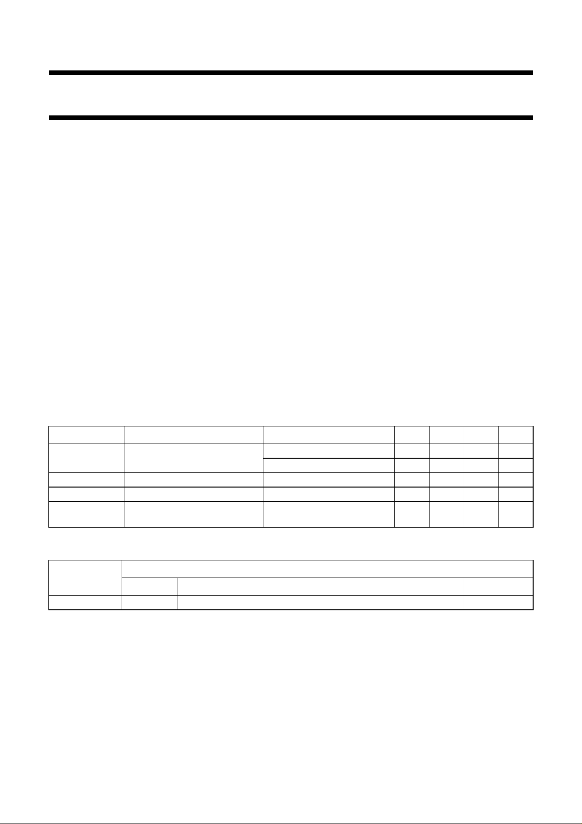
QUICK REFERENCE DATA
GENERAL DESCRIPTION
The TJA1010 is an octal low side driver for relays in
automotive applications.
SYMBOL PARAMETER CONDITIONS MIN. TYP. MAX. UNIT
V
DD
supply voltage operating 5.5 − 25 V
load dump −−50 V
V
o(clamp)
R
o(on)
I
o
drain-to-source clamp voltage Io=20mA 506070V
on resistance Io= 0.2 A −−3Ω
output current continuous at all outputs;
T
=85°C
amb
−−0.2 A
ORDERING INFORMATION
TYPE
NUMBER
NAME DESCRIPTION VERSION
PACKAGE
TJA1010T SO28 plastic small outline package; 28 leads; body width 7.5 mm SOT136-1
1998 Feb 09 2
This text is here in white to force landscape pages to be rotated correctly when browsing through the pdf in the Acrobat reader.This text is here in
_white to force landscape pages to be rotated correctly when browsing through the pdf in the Acrobat reader.This text is here inThis text is here in
white to force landscape pages to be rotated correctly when browsing through the pdf in the Acrobat reader. white to force landscape pages to be ...
1998 Feb 09 3
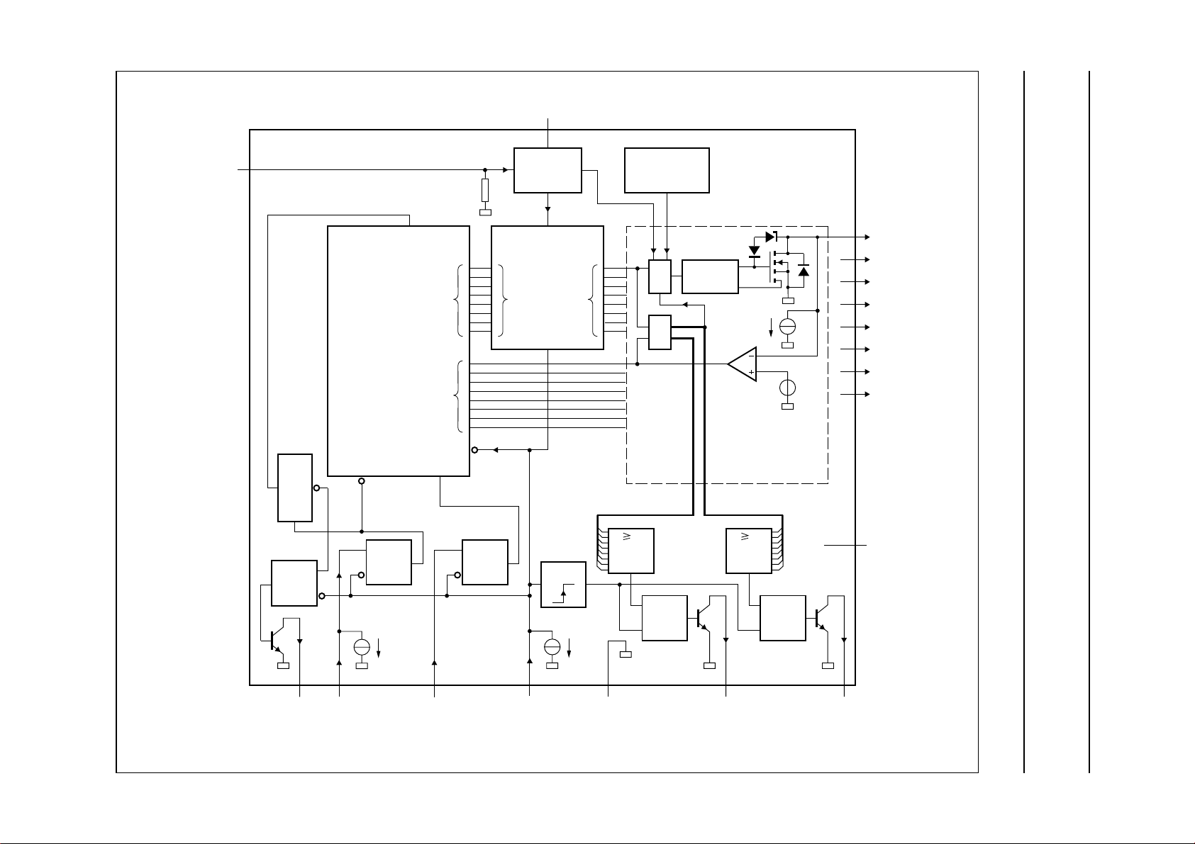
handbook, full pagewidth
STBY
25
serial input
parallel
outputs
8-BIT
SHIFT
REGISTER
parallel
inputs
V
DD
SUPPLY
AND
REFERENCE
master
reset
8-BIT
LATCH
data
inputs
clock
24
UV
power-on
data
outputs
0 V
TEMPERATURE
PROTECTION
CURRENT
LIMITING
TJA1010
1
OUT1
3
OUT2
12
OUT3
14
OUT4
15
OUT5
17
OUT6
26
V
ref
OUT7
28
OUT8
BLOCK DIAGRAM
Octal Low Side Driver (OLSD) TJA1010
Philips Semiconductors Preliminary specification
latch
DQ
clock
&
serial clock
&
parallel
load
serial input
&
DELAY
T
stat
115410
Fig.1 Block diagram.
OL SC
1 1
&
6 to 9
20 to 23
2, 13
16, 27
GND1
to
GND4
&
19
MBH994
18
STATSCSTATOLGNDSIESISCLSO
Philips Semiconductors Preliminary specification
Octal Low Side Driver (OLSD) TJA1010
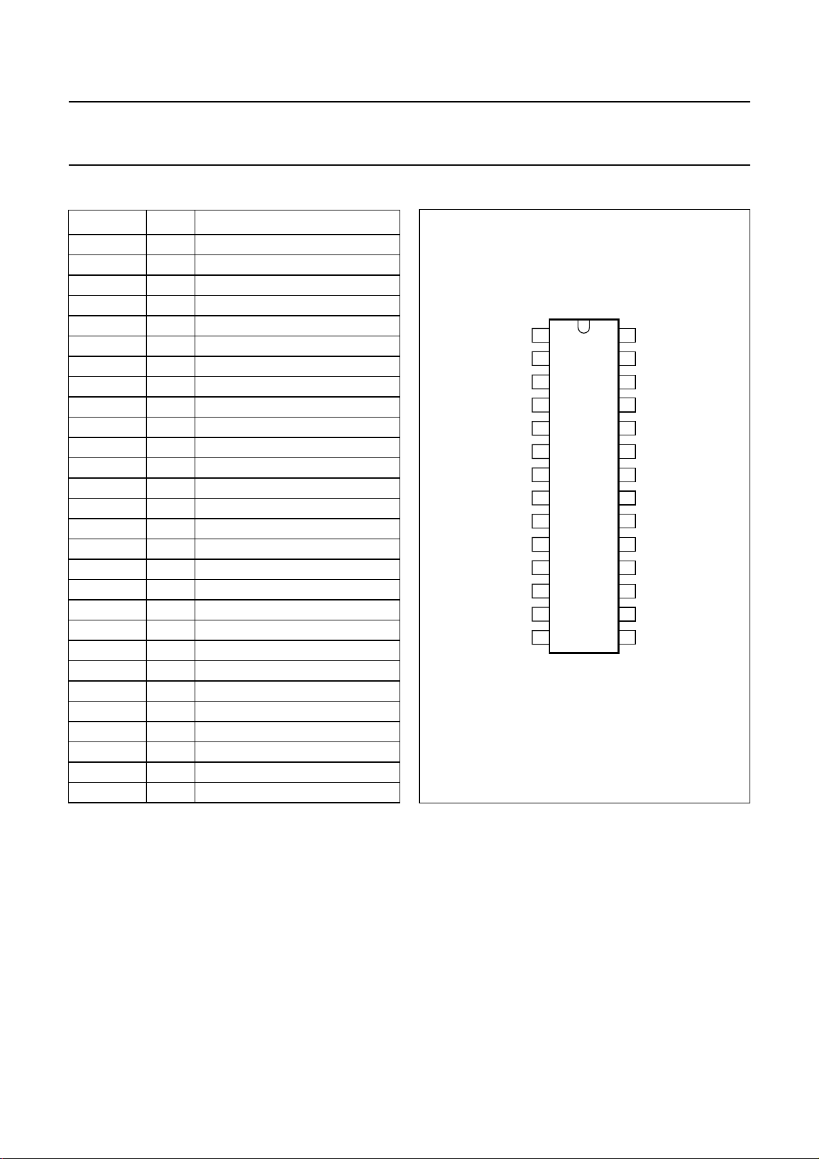
PINNING
SYMBOL PIN DESCRIPTION
OUT1 1 output 1
GND1 2 ground 1
OUT2 3 output 2
SCL 4 serial clock input
SI 5 serial input
GND 6 ground
GND 7 ground
GND 8 ground
GND 9 ground
SO 10 serial output
SIE 11 serial input enable
OUT3 12 output 3
GND2 13 ground 2
OUT4 14 output 4
OUT5 15 output 5
GND3 16 ground 3
OUT6 17 output 6
STATSC 18 status output short-circuited load
STATOL 19 status output open load
GND 20 ground
GND 21 ground
GND 22 ground
GND 23 ground
V
DD
24 supply voltage
STBY 25 standby input
OUT7 26 output 7
GND4 27 ground 4
OUT8 28 output 8
handbook, halfpage
OUT1
1
GND1
2
OUT2
3
SCL
4
SI
5
GND
6
GND
7
TJA1010
8
GND
GND
9
SO
10
SIE
11
OUT3
12
GND2
13
OUT4
MBH990
Fig.2 Pin configuration.
28
27
26
25
24
23
22
21
20
19
18
17
16
1514
OUT8
GND4
OUT7
STBY
V
DD
GND
GND
GND
GND
STATOL
STATSC
OUT6
GND3
OUT5
1998 Feb 09 4

Philips Semiconductors Preliminary specification
Octal Low Side Driver (OLSD) TJA1010
FUNCTIONAL DESCRIPTION (see Figs 1, 3 and 4) This octal low side driver is intended to drive relays in
automotive applications. It is optimized to withstand the
wide temperature and supply voltage range that is typical
for this application area. It consists of 8 protected outputs,
including diagnostic functions, controlled by a serial
interface. These outputs can be used in parallel without the
need for additional components.
Serial control interface
Serial control of the drivers is provided by an 8-bit shift
register with parallel outputs and an 8-bit latch which
controls the DMOS output stages. Using this configuration
the number of pins needed for control of the eight drivers
is reduced to three; Serial Input (SI), Serial CLock (SCL)
and Serial Input Enable (SIE). When pin SIE is LOW, serial
data at pin SI is shifted into the shift register at each
HIGH-to-LOW transition at the SCL pin and serial data is
shifted out at the Serial Output (SO) pin at a LOW-to-HIGH
transition on the SCL pin. The last bit read in before a
LOW-to-HIGH transition at the SIE pin is bit D8. A HIGH
level at the SI pin causes a driver to switch-on. With a
LOW-to-HIGH transition at the SIE pin, parallel output data
in the shift register is written to the 8-bit latch, which
controls the DMOS outputs. When SIE is HIGH, signals at
pins SI, SCL and SO are disabled. For pin SO this results
in a HIGH level because pin SO is an open-collector
output.
Diagnostic interface
The OLSD detects open loads and short-circuited loads at
each driver stage by comparing its output voltages (V
a reference voltage (V
). To allow distinction between
ref
o
) to
short-circuit and open load conditions, a short-circuit is
detected for Vo>V
detected for Vo<V
in the on-state, while an open load is
ref
in the off-state of a driver stage.
ref
In both cases the corresponding status pin is set to a LOW
level and the respective bit in the shift register is inverted
on a HIGH-to-LOW transition of SIE.
By writing a following byte into the shift register, its actual
contents (the control byte eventually modified by errors)
can be read out via pin SO. Comparing this byte with the
original control byte previously written, faults can be
localized and identified (e.g. open load at driver stage
number 5).
Protection of DMOS outputs
Each driver contains a DMOS power FET. The drivers are
protected against overvoltage, short-circuit and
overtemperature conditions.
An overvoltage clamp circuit at each driver causes the
respective DMOS power FET to turn partially on, if its
drain-to-source voltage level exceeds the clamp level
[V
]. Consequently each driver can withstand
o(clamp)
voltage peaks caused by turning off inductive loads, such
as relays coils without freewheel diodes. It should be noted
that if outputs are used in parallel the amount of inductive
energy which can be handled will not increase but will
remain equal to that of a single output.
Each driver is protected against a short-circuited load by
current limiting. In the event of a short-circuited load at a
driver stage, the current will be limited and the HIGH level
of its drain-to-source voltage will force the comparator
output to go HIGH. This in turn will set the STATSC pin to
a LOW level.
A two-stage temperature protection circuit is included to
protect the device against overheating caused by high
dissipation in the output transistors.
When the temperature exceeds the overtemperature
threshold level, it will switch-off those outputs with a
short-circuit condition for the duration of the
overtemperature condition. The status and diagnostic
function will not be influenced.
If the chip temperature still rises and exceeds the
emergency threshold level, the emergency shutdown will
become active and shut down all of the outputs until the
temperature drops below the overtemperature threshold.
The outputs are fully protected against short-circuit to
battery conditions for the whole supply voltage range.
To protect the outputs against device threatening
dissipation peaks, the overtemperature control is extended
with local power dissipation sensors. If one or more
outputs dissipate too much power all outputs with a
short-circuit condition will be switched off for the duration
of the local overtemperature condition.
To protect the outputs against high dissipation during load
dump, an overvoltage protection is included. This will
switch-off those outputs with a short-circuit condition if the
supply voltage exceeds the overvoltage threshold V
DD(0 V)
for the duration of the overvoltage condition.
The diagnostic and status information will not change due
to the interference of the overvoltage and overtemperature
protections.
To avoid a false LOW signal at the SC pin due to switching
transients at the DMOS outputs, the SC pin is disabled for
a sufficient delay time whenever a new input control byte
has been written into the 8-bit latch with a LOW-to-HIGH
transition of SIE.
1998 Feb 09 5

Philips Semiconductors Preliminary specification
Octal Low Side Driver (OLSD) TJA1010
Other features
When using several OLSDs, input control and diagnostics
can be provided, as described above, without spending
further microcontroller pins by cascading, i.e. connecting
A power-on reset ensures a defined off state for all drivers
when the device is switched on i.e. by switching on the
power supply or by activating the device via the STBY pin.
Thus the STBY input can also be used as a reset pin.
the SO pin of one OLSD to the SI pin of the following
OLSD.
A standby input (STBY) pin allows the off state current
consumption in the OLSD to be minimized. Thus the OLSD
can be connected permanently to a battery.
LIMITING VALUES
In accordance with the Absolute Maximum Rating System (IEC 134).
SYMBOL PARAMETER CONDITIONS MIN. MAX. UNIT
V
DD
supply voltage continuous 0 25 V
transient 0 50 V
V
n
V
I(STBY)
V
o(STAT
input voltage at pins SI, SCL and SIE 0 5.5 V
input voltage at pin STBY 0 7 V
) output voltage at pins STATOL and
018V
STATSC
V
o(SO)
I
o
I
o(con)
I
clamp(rep)
output voltage at pin SO 0 18 V
output current internally limited
continuous output current Tj= 135 °C −0.2 +0.2 A
T
=95°C −0.3 +0.3 A
j
repetitive inductive turn-off current per
Tj= 135 °C; note 1 see Fig.5 A
output
E
clamp(rep)
repetitive inductive turn-off energy per
Tj=95°C; notes 1 and 2 − 5mJ
output
E
clamp(nrep)
non-repetitive inductive turn-off
Tj=95°C; notes 1 and 3 − 60 mJ
energy per output
T
vj
T
stg
V
esd
virtual junction temperature −40 +135 °C
storage temperature −55 +150 °C
electrostatic handling human body model − 3kV
machine model − 300 V
Notes
1. The amount of E
used in parallel it can handle the E
2. Defined for t
3. Defined for t
clamp
clamp
per output can NOT be added if outputs are used in parallel. Thus, if two or more outputs are
clamp
of one output.
clamp
= 1 ms.
= 5 ms.
1998 Feb 09 6

Philips Semiconductors Preliminary specification
Octal Low Side Driver (OLSD) TJA1010
THERMAL CHARACTERISTICS
SYMBOL PARAMETER CONDITIONS VALUE UNIT
R
th (j-amb)
R
th (j-sp)
Notes
1. Printed on an FR-4 board with minimum foot print.
2. Power uniformly divided over all outputs.
CHARACTERISTICS
= −40 to +135 °C; VDD= 11 to 13.5 V; V
T
j
Positive currents flow into the IC. All parameters are guaranteed over the temperature range by design, but only 100%
tested at T
SYMBOL PARAMETER CONDITIONS MIN. TYP. MAX. UNIT
I
DD
V
DD(UV)
V
DD(0V)
V
o(clamp)
I
LO
I
o(lim)
R
o
V
ref
δI
/δt maximum rise and fall time of
o
V
IH
V
i(hys)
V
IL
V
IL(STBY)
from junction to ambient in free air note 1 55 K/W
from junction to soldering point of ground pins
note 2 17 K/W
6 to 9 and 20 to 23
bat(max)=VDD
=25°C; unless otherwise specified.
amb
supply current Io= 0 mA; V
+ 1.5 V. All voltages are defined with respect to ground.
>3V −−5mA
STBY
<1V; VDD=13V;
V
STBY
−−10 µA
Tj=−40 to +85 °C
undervoltage shutdown threshold 2 − 4.3 V
overvoltage protection threshold 25 − 33 V
output clamp voltage Io=20mA 506070V
output leakage current
(one output)
off-state, Vo= 13 V; standby − 10 µA
off-state, V
=13V;
o
70 − 210 µA
operational
off-state, V
=1V;
o
40 − 180 µA
operational
output current limit (one output) on-state 0.3 − 0.55 A
output resistance (one output) Io= 0.2 A; VDD=13V;
−−3Ω
Tj= 135 °C
I
= 0.2 A; VDD=13V;
o
−−2.5 Ω
Tj=25°C
I
= 0.1 A; VDD= 5.5 V;
o
−−10 Ω
see Fig.6
open load/short-circuit reference
note 1 1 − 1.9 V
voltage
output current
HIGH-level input voltage at pins
VDD=13V; RL= 100 Ω;
note 2
−−100 mA/µs
3 −−V
SI, SCL, SIE and STBY
input voltage hysteresis at pins
note 2 0.2 − 1.2 V
SI, SCL and SIE
LOW-level input voltage at pins
−−0.8 V
SI, SCL and SIE
LOW-level input voltage at pin
−−1V
STBY
1998 Feb 09 7

Philips Semiconductors Preliminary specification
Octal Low Side Driver (OLSD) TJA1010
SYMBOL P ARAMETER CONDITIONS MIN. TYP . MAX. UNIT
I
i
I
LI
R
i(STBY)
I
i(STBY)
V
STAT(L)
V
SO(L)
I
LO(SO)
f
clk
t
W(SCL)
t
d(SIE-SCL)
t
su(SIE-SCL)
t
d(SCL-SO)
t
su(SI-SCL)
t
h(SCL-SI)
t
h(SCL-SIE)
t
su(STBY)
t
h(STBY)
t
d(STAT)
T
th(otc)
T
th(ets)
input current at pins SCL and SIE Vi=3V 20 − 60 µA
input leakage current at pins SI,
SIE and SCl
off-state; Vi=3V;
Tj=85°C; V
STBY
−−5µA
<1V
input resistance at pin STBY Vi=1V; Tj<85°C40−150 kΩ
input current at pin STBY Vi=3V 20 − 60 µA
status LOW voltage I
= 1.6 mA −−0.4 V
STAT(L)
serial output LOW voltage ISO= 1.6 mA −−0.4 V
output leakage current at pin SO
and status outputs
off-state; Vo=5V;
V
<1V; Tj<85°C
STBY
−−10 µA
clock frequency −−1 MHz
SCL positive pulse width HIGH-to-LOW transition 500 −−ns
delay time from SIE HIGH to SCL
100 −−ns
LOW
set-up time from SIE LOW to SCL
250 −−ns
HIGH
delay time from SCL HIGH to SO
note 3 −−250 ns
valid
set-up time from SI to falling edge
150 −−ns
of SCL
hold time from falling edge of SCL
150 −−ns
to SI
hold time from SCL LOW to SIE
250 −−ns
HIGH
STBY set-up time from STBY
100 −−µs
HIGH to SIE LOW
STBY hold time from SIE HIGH to
10 −−µs
STBY LOW
delay time for status pin enable 40 100 250 µs
threshold overtemperature control − 170 −°C
threshold emergency temperature
− 190 −°C
shutdown
Notes
1. Open load is indicated for Vo<V
in the off-state, short-circuited load is indicated for Vo>V
ref
2. Guaranteed by design.
3. Delay caused by load excluded.
1998 Feb 09 8
in the on-state.
ref

Philips Semiconductors Preliminary specification
Octal Low Side Driver (OLSD) TJA1010
handbook, full pagewidth
(1) Inverting only when error (open load/short-circuit).
SIE
SCL
shift
register
bit n
SI
SO
OUT2 corresponding to D8 old
previous
D8
B
(1)
n+1
D1
new
D1
old
D2
new
D2
old
D3
D4
new
newD5newD6newD7newD8new
D3
D4
old
oldD5oldD6oldD7oldD8old
corresponding to D1 oldOUT1
corresponding to D1 new
corresponding to D8 new
MBH992
Fig.3 Serial interface timing.
1998 Feb 09 9

Philips Semiconductors Preliminary specification
Octal Low Side Driver (OLSD) TJA1010
ndbook, full pagewidth
STBY
SIE
SCL
SI
SO
t
su(STBY)
t
d(SIE-SCL)
don't care
t
h(STBY)
previous
t
d(SCL-SO)
t
w(SCL)
t
su(SI-SCL)
valid
valid
t
d(SCL-SIE)
t
h(SCL-SI)
Fig.4 Input and output waveform timing.
70%
16%
70%
16%
70%
16%
70%
16%
5 V
0 V
5 V
0 V
5 V
0 V
5 V
0 V
5 V
0 V
MBH993
0.16
handbook, full pagewidth
I
clamp
(A)
0.14
0.12
0.10
0.08
0.06
0.04
0.02
0
0
The curve is based on behaviour of relays; Siemens A4001-X40.
100 200 300 400 500
Fig.5 Maximum current during inductive turn-off (T
amb
=85°C).
t (µs)
MGL379
600
1998 Feb 09 10

Philips Semiconductors Preliminary specification
Octal Low Side Driver (OLSD) TJA1010
12
handbook, full pagewidth
R
on
(Ω)
10
8
6
4
2
0
56
MGL380
789 11121314
10
V
(V)
DD
Fig.6 Maximum on-resistance as a function of supply voltage.
15
handbook, full pagewidth
MICROCONTROLLER
+
5 V
REGULATOR
+
5 V
R1
STBY
SIE
SCL
SI
R3R2
SO
STATSC
OL
Fig.7 Application example.
1998 Feb 09 11
V
DD
TJA1010
GND
100 nF 100 µF
C2 C1
OUT1
OUT2
OUT3
OUT4
OUT5
OUT6
OUT7
OUT8
D1
load
load
load
load
load
load
load
load
MBH991
V
bat

Philips Semiconductors Preliminary specification
Octal Low Side Driver (OLSD) TJA1010
PACKAGE OUTLINE
SO28: plastic small outline package; 28 leads; body width 7.5 mm
D
c
y
Z
28
pin 1 index
1
e
15
14
w M
b
p
SOT136-1
E
H
E
Q
A
2
A
1
L
p
L
detail X
(A )
A
X
v M
A
A
3
θ
0 5 10 mm
scale
DIMENSIONS (inch dimensions are derived from the original mm dimensions)
UNIT
mm
inches
Note
1. Plastic or metal protrusions of 0.15 mm maximum per side are not included.
A
max.
2.65
0.10
OUTLINE
VERSION
SOT136-1
A
1
0.30
0.10
0.012
0.004
A2A
2.45
2.25
0.096
0.089
IEC JEDEC EIAJ
075E06 MS-013AE
0.25
0.01
b
3
p
0.49
0.32
0.36
0.23
0.019
0.013
0.014
0.009
(1)E(1) (1)
cD
18.1
7.6
7.4
0.30
0.29
1.27
0.050
17.7
0.71
0.69
REFERENCES
1998 Feb 09 12
eHELLpQ
10.65
10.00
0.419
0.394
1.4
0.055
1.1
0.4
0.043
0.016
1.1
1.0
0.043
0.039
PROJECTION
0.25
0.25 0.1
0.01
0.01
EUROPEAN
ywv θ
Z
0.9
0.4
0.035
0.004
0.016
ISSUE DATE
95-01-24
97-05-22
o
8
o
0

Philips Semiconductors Preliminary specification
Octal Low Side Driver (OLSD) TJA1010
SOLDERING
Introduction
There is no soldering method that is ideal for all IC
packages. Wave soldering is often preferred when
through-hole and surface mounted components are mixed
on one printed-circuit board. However, wave soldering is
not always suitable for surface mounted ICs, or for
printed-circuits with high population densities. In these
situations reflow soldering is often used.
This text gives a very brief insight to a complex technology.
A more in-depth account of soldering ICs can be found in
our
“IC Package Databook”
Reflow soldering
Reflow soldering techniques are suitable for all SO
packages.
Reflow soldering requires solder paste (a suspension of
fine solder particles, flux and binding agent) to be applied
to the printed-circuit board by screen printing, stencilling or
pressure-syringe dispensing before package placement.
Several techniques exist for reflowing; for example,
thermal conduction by heated belt. Dwell times vary
between 50 and 300 seconds depending on heating
method. Typical reflow temperatures range from
215 to 250 °C.
Preheating is necessary to dry the paste and evaporate
the binding agent. Preheating duration: 45 minutes at
45 °C.
(order code 9398 652 90011).
Wave soldering
Wave soldering techniques can be used for all SO
packages if the following conditions are observed:
• A double-wave (a turbulent wave with high upward
pressure followed by a smooth laminar wave) soldering
technique should be used.
• The longitudinal axis of the package footprint must be
parallel to the solder flow.
• The package footprint must incorporate solder thieves at
the downstream end.
During placement and before soldering, the package must
be fixed with a droplet of adhesive. The adhesive can be
applied by screen printing, pin transfer or syringe
dispensing. The package can be soldered after the
adhesive is cured.
Maximum permissible solder temperature is 260 °C, and
maximum duration of package immersion in solder is
10 seconds, if cooled to less than 150 °C within
6 seconds. Typical dwell time is 4 seconds at 250 °C.
A mildly-activated flux will eliminate the need for removal
of corrosive residues in most applications.
Repairing soldered joints
Fix the component by first soldering two diagonallyopposite end leads. Use only a low voltage soldering iron
(less than 24 V) applied to the flat part of the lead. Contact
time must be limited to 10 seconds at up to 300 °C. When
using a dedicated tool, all other leads can be soldered in
one operation within 2 to 5 seconds between
270 and 320 °C.
1998 Feb 09 13

Philips Semiconductors Preliminary specification
Octal Low Side Driver (OLSD) TJA1010
DEFINITIONS
Data sheet status
Objective specification This data sheet contains target or goal specifications for product development.
Preliminary specification This data sheet contains preliminary data; supplementary data may be published later.
Product specification This data sheet contains final product specifications.
Limiting values
Limiting values given are in accordance with the Absolute Maximum Rating System (IEC 134). Stress above one or
more of the limiting values may cause permanent damage to the device. These are stress ratings only and operation
of the device at these or at any other conditions above those given in the Characteristics sections of the specification
is not implied. Exposure to limiting values for extended periods may affect device reliability.
Application information
Where application information is given, it is advisory and does not form part of the specification.
LIFE SUPPORT APPLICATIONS
These products are not designed for use in life support appliances, devices, or systems where malfunction of these
products can reasonably be expected to result in personal injury. Philips customers using or selling these products for
use in such applications do so at their own risk and agree to fully indemnify Philips for any damages resulting from such
improper use or sale.
1998 Feb 09 14

Philips Semiconductors Preliminary specification
Octal Low Side Driver (OLSD) TJA1010
NOTES
1998 Feb 09 15

Philips Semiconductors – a worldwide company
Argentina: see South America
Australia: 34 Waterloo Road, NORTH RYDE, NSW 2113,
Tel. +61 2 9805 4455, Fax. +61 29805 4466
Austria: Computerstr. 6, A-1101 WIEN, P.O. Box 213, Tel. +43 160 1010,
Fax. +43 160 101 1210
Belarus: Hotel Minsk Business Center, Bld. 3, r. 1211, Volodarski Str. 6,
220050 MINSK, Tel. +375 172 200 733, Fax. +375 172 200773
Belgium: see The Netherlands
Brazil: seeSouth America
Bulgaria: Philips Bulgaria Ltd., Energoproject, 15thfloor,
51 James Bourchier Blvd., 1407 SOFIA,
Tel. +359 2 689 211, Fax. +359 2689 102
Canada: PHILIPS SEMICONDUCTORS/COMPONENTS,
Tel. +1 800 234 7381
China/Hong Kong: 501 Hong Kong Industrial Technology Centre,
72 Tat Chee Avenue, Kowloon Tong, HONG KONG,
Tel. +852 2319 7888, Fax. +8522319 7700
Colombia: see South America
Czech Republic: see Austria
Denmark: Prags Boulevard 80, PB 1919, DK-2300 COPENHAGEN S,
Tel. +45 32 88 2636, Fax. +45 31 57 0044
Finland: Sinikalliontie 3, FIN-02630 ESPOO,
Tel. +358 9 615800, Fax. +358 9 61580920
France: 51 Rue Carnot, BP317, 92156 SURESNES Cedex,
Tel. +33 1 40 99 6161, Fax. +33 1 4099 6427
Germany: Hammerbrookstraße 69, D-20097 HAMBURG,
Tel. +49 40 23 53 60, Fax. +4940 23536 300
Greece: No. 15, 25th March Street, GR 17778 TAVROS/ATHENS,
Tel. +30 1 4894 339/239, Fax. +30 14814 240
Hungary: seeAustria
India: Philips INDIA Ltd, Band Box Building, 2nd floor,
254-D, Dr. Annie BesantRoad, Worli, MUMBAI 400 025,
Tel. +91 22 493 8541, Fax.+91 22493 0966
Indonesia: see Singapore
Ireland: Newstead, Clonskeagh, DUBLIN 14,
Tel. +353 1 7640 000, Fax.+353 17640 200
Israel: RAPAC Electronics, 7 Kehilat Saloniki St, PO Box 18053,
TEL AVIV 61180, Tel. +972 3 645 0444, Fax.+972 3649 1007
Italy: PHILIPS SEMICONDUCTORS, Piazza IV Novembre 3,
20124 MILANO, Tel. +39 2 6752 2531, Fax. +39 2 6752 2557
Japan: Philips Bldg 13-37, Kohnan 2-chome, Minato-ku, TOKYO 108,
Tel. +81 3 3740 5130, Fax. +81 33740 5077
Korea: Philips House, 260-199 Itaewon-dong, Yongsan-ku, SEOUL,
Tel. +82 2 709 1412, Fax. +82 2 709 1415
Malaysia: No. 76 Jalan Universiti, 46200 PETALING JAYA, SELANGOR,
Tel. +60 3 750 5214, Fax. +60 3 7574880
Mexico: 5900 Gateway East, Suite 200, EL PASO, TEXAS 79905,
Tel. +9-5 800 234 7381
Middle East: see Italy
Netherlands: Postbus 90050, 5600PB EINDHOVEN, Bldg. VB,
Tel. +31 40 27 82785, Fax. +31 4027 88399
New Zealand: 2 Wagener Place, C.P.O. Box 1041, AUCKLAND,
Tel. +64 9 849 4160, Fax. +64 9 849 7811
Norway: Box 1, Manglerud 0612, OSLO,
Tel. +47 22 74 8000, Fax. +47 22 74 8341
Philippines: Philips Semiconductors Philippines Inc.,
106 Valero St. Salcedo Village, P.O. Box 2108 MCC,MAKATI,
Metro MANILA, Tel. +63 2 816 6380, Fax. +632 817 3474
Poland: Ul. Lukiska 10, PL 04-123 WARSZAWA,
Tel. +48 22 612 2831, Fax.+48 22612 2327
Portugal: see Spain
Romania: see Italy
Russia: Philips Russia, Ul. Usatcheva 35A, 119048 MOSCOW,
Tel. +7 095 755 6918, Fax.+7 095755 6919
Singapore: Lorong 1, Toa Payoh, SINGAPORE 1231,
Tel. +65 350 2538, Fax. +65 251 6500
Slovakia: see Austria
Slovenia: see Italy
South Africa: S.A. PHILIPS Pty Ltd., 195-215 Main Road Martindale,
2092 JOHANNESBURG, P.O. Box 7430 Johannesburg 2000,
Tel. +27 11 470 5911, Fax.+27 11470 5494
South America: Al. Vicente Pinzon, 173, 6th floor,
04547-130 SÃO PAULO, SP, Brazil,
Tel. +55 11 821 2333, Fax.+55 11821 2382
Spain: Balmes 22, 08007 BARCELONA,
Tel. +34 3 301 6312, Fax. +34 3 301 4107
Sweden: Kottbygatan 7, Akalla, S-16485 STOCKHOLM,
Tel. +46 8 632 2000, Fax. +46 8 632 2745
Switzerland: Allmendstrasse 140, CH-8027 ZÜRICH,
Tel. +41 1 488 2686, Fax. +41 1 488 3263
Taiwan: Philips Semiconductors, 6F, No. 96, Chien Kuo N. Rd., Sec. 1,
TAIPEI, Taiwan Tel. +886 2 2134 2865, Fax. +886 2 2134 2874
Thailand: PHILIPS ELECTRONICS (THAILAND) Ltd.,
209/2 Sanpavuth-Bangna Road Prakanong, BANGKOK 10260,
Tel. +66 2 745 4090, Fax. +66 2 398 0793
Turkey: Talatpasa Cad. No. 5, 80640 GÜLTEPE/ISTANBUL,
Tel. +90 212 279 2770, Fax. +90 212 282 6707
Ukraine: PHILIPS UKRAINE, 4 Patrice Lumumba str., Building B, Floor 7,
252042 KIEV, Tel. +380 44 264 2776, Fax. +38044 268 0461
United Kingdom: Philips Semiconductors Ltd., 276 Bath Road, Hayes,
MIDDLESEX UB3 5BX, Tel. +44 181 730 5000, Fax.+44 181754 8421
United States: 811 East Arques Avenue, SUNNYVALE, CA 94088-3409,
Tel. +1 800 234 7381
Uruguay: see South America
Vietnam: see Singapore
Yugoslavia: PHILIPS, Trg N. Pasica 5/v, 11000 BEOGRAD,
Tel. +381 11 625 344, Fax.+38111 635777
For all other countries apply to: Philips Semiconductors,
International Marketing & Sales Communications, Building BE-p, P.O. Box 218,
5600 MD EINDHOVEN, The Netherlands, Fax. +31 40 27 24825
© Philips Electronics N.V. 1998 SCA57
All rights are reserved. Reproduction in whole or in part is prohibited without the prior written consent of the copyright owner.
The information presented in this document does not form part of any quotation or contract, is believed to be accurate and reliable and may be changed
without notice. No liability will be accepted by the publisher for any consequence of its use. Publication thereof does not convey nor imply any license
under patent- or other industrial or intellectual property rights.
Internet: http://www.semiconductors.philips.com
Printed in The Netherlands 615102/00/01/pp16 Date of release: 1998 Feb 09 Document order number: 9397 750 01763
 Loading...