


INTEGRATED CIRCUITS
DATA SH EET
TDA9820
Multistandard/dual channel TV FM
intercarrier sound demodulator
Product specification
Supersedes data of March 1991
File under Integrated Circuits, IC02
1996 Nov 20
Philips Semiconductors Product specification
Multistandard/dual channel TV FM
TDA9820
intercarrier sound demodulator
FEATURES
• Multistandard application for sound standards M, B/G, I
and D/K
• Two alignment-free PLL FM demodulators
• Four-input source selector for one of the two FM
demodulators
• Automatic second sound carrier mute
• Mono and dual channel application
• Low power consumption
• Few external components required.
QUICK REFERENCE DATA
SYMBOL PARAMETER CONDITIONS MIN. TYP. MAX. UNIT
V
P
I
P
I
M
V
i(rms)
V
o(rms)
SN+
-------------N
α
8/7
supply voltage (pin 14) 4.5 5.0 8.8 V
supply current (pin 14) 23 30 37 mA
AC peak current (pins 7 and 8) −−1.5 mA
input signal (RMS value) − 150 250 µV
output signal (pins 7 and 8; RMS value) ∆fi= ±50 kHz 0.4 0.5 0.6 V
signal plus noise-to-noise ratio
(pins 7 and 8)
crosstalk attenuation f = 50 to 12500 Hz 60 70 − dB
RR supply voltage ripple rejection
(pins 7 and 8)
T
amb
operating ambient temperature 0 − 70 °C
GENERAL DESCRIPTION
The TDA9820 is a monolithic, integrated, multistandard TV
FM intercarrier sound demodulator for all FM standards.
The circuit contains two separate FM demodulators using
Phase Locked Loop (PLL) reference frequency
generation. The circuit requires a minimum number of
external components.
SN+
--------------
in accordance with
N
40 dB=
64 68 − dB
“CCIR 468-3”
< 200 mV; f = 70 Hz 16 20 − dB
V
RR
ORDERING INFORMATION
PACKAGE
TYPE NUMBER
NAME DESCRIPTION VERSION
TDA9820 DIP16 plastic dual in-line package; 16 leads (300 mil); long body SOT38-1
TDA9820T SO16 plastic small outline package; 16 leads; body width 7.5 mm SOT162-1
1996 Nov 20 2
Philips Semiconductors Product specification
Multistandard/dual channel TV FM
intercarrier sound demodulator
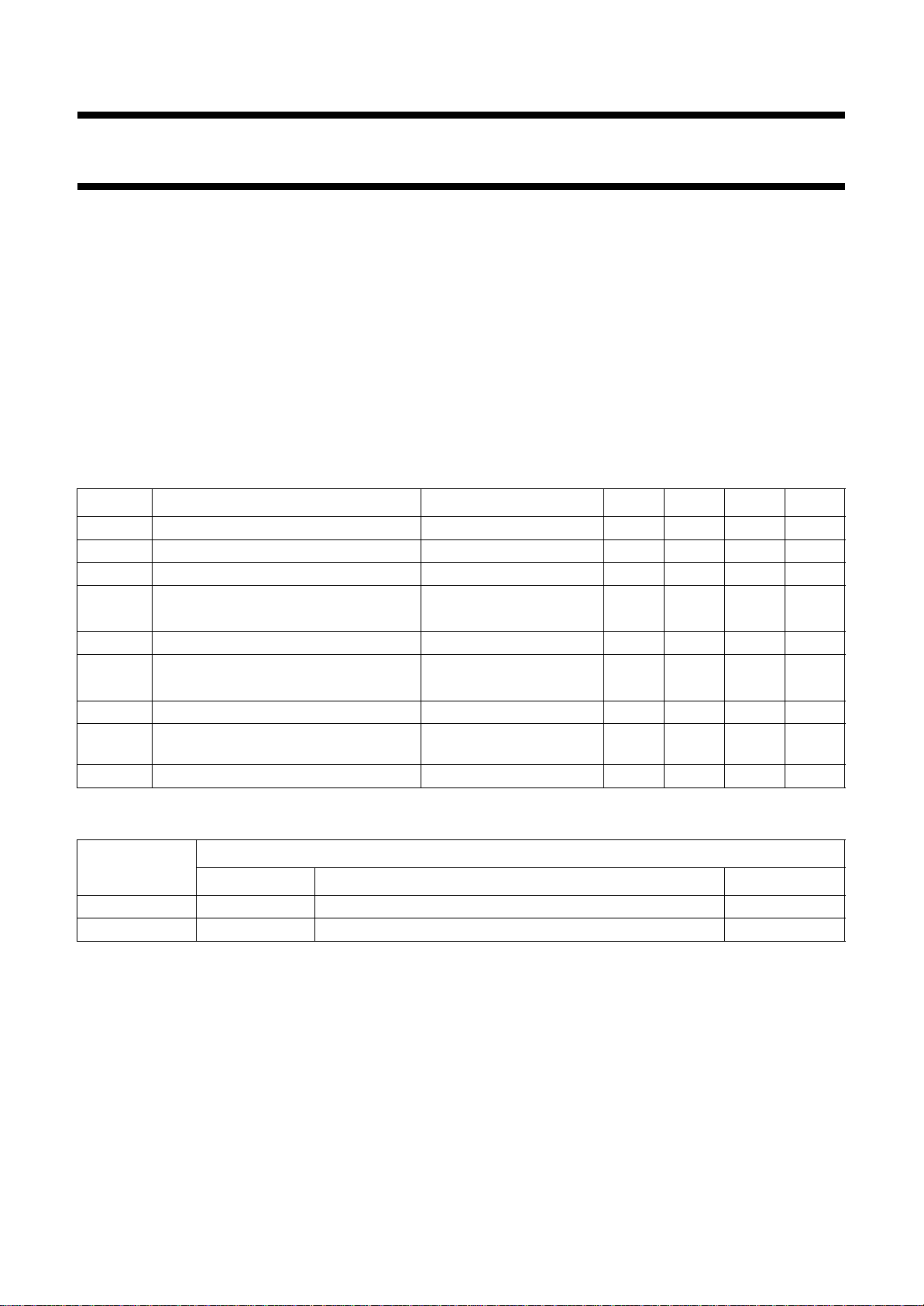
BLOCK DIAGRAM
handbook, full pagewidth
intercarrier
4.5 MHz (M)
5.5 MHz (B/G)
6.0 MHz (I)
6.5 MHz (D/K)
4.72 MHz (M)
or
5.74 MHz (B/G)
or
6.74 MHz (D/K)
3
1
16
2
15
SUPPLY
V =
P
4.5 to 8.8 V
TDA9820
7-STAGE
LIMITER
AMPLIFIER 1
7-STAGE
LIMITER
AMPLIFIER 2
11121413
VCO
ref
mute
R
s
VCO 1
VCO 2
optional stereo
channel separation
adjustment
(1)
R
(1)
pot
9
CONTROL
UNIT
10
+
−
−
+
MHA420
TDA9820
8
V
AF1
S
5
1
S
6
2
7
V
AF2
standard
switch
(1) Resistor and potentiometer between capacitor and earth are inserted if adjustment of stereo channel separation is required.
1996 Nov 20 3
Fig.1 Block diagram.
Philips Semiconductors Product specification
Multistandard/dual channel TV FM
intercarrier sound demodulator
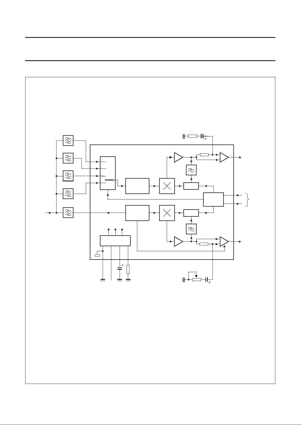
PINNING
SYMBOL PIN DESCRIPTION
IN
1(B/G)
IN
1(D/K)
IN
1(M)
n.c. 4 not connected
S
1
S
2
V
AF2
V
AF1
C
1
C
2
VCO
ref
C
STAB
GND 13 ground
V
P
IN
2
IN
1(I)
1 intercarrier input 1 at 5.5 MHz
2 intercarrier input 1 at 6.5 MHz
3 intercarrier input 1 at 4.5 MHz
5 standard switch bit 1 input
6 standard switch bit 2 input
7 audio output voltage 2
8 audio output voltage 1
9 decoupling capacitor 1
10 decoupling capacitor 2
11 VCO reference
12 supply voltage stabilization
14 supply voltage
15 intercarrier input 2
16 intercarrier input 1 at 6.0 MHz
handbook, halfpage
IN
IN
1(B/G)
1(D/K)
IN
1(M)
n.c.
V
AF2
V
AF1
1
2
3
4
1
2
5
6
7
8
TDA9820
MHA529
S
S
Fig.2 Pin configuration.
TDA9820
IN
16
1(I)
IN
15
2
V
14
P
13
GND
C
12
STAB
VCO
11
ref
C
10
2
C
9
1
1996 Nov 20 4
Philips Semiconductors Product specification
Multistandard/dual channel TV FM
intercarrier sound demodulator
FUNCTIONAL DESCRIPTION
The complete circuit consists of two separate channels,
each consisting of a limiter-amplifier, FM demodulator and
AF amplifier. Circuit operation is also described in Fig.1.
Source selector
The intercarrier signal is fed through external ceramic
band-pass filters which are tuned to the sound carrier
frequencies.
One of the four filtered sound carriers from
pins 1, 2, 3 or 16 is fed to limiter-amplifier 1 via the
appropriate electronic switch in the source selector.
The electronic switch of the sound carrier is selected by
the control unit (see Table 1).
The second sound carrier of the intercarrier signal is
directly fed from pin 15 to limiter-amplifier 2.
FM demodulators
TDA9820
Stereo channel separation adjustment (optional)
Optimal stereo channel separation is achieved by
adjusting V
1. V
AF1
capacitor at pin 9
2. V
AF2
DC decoupling capacitor on pin 10 to the same
voltage as V
Second sound carrier mute
The output of the second FM demodulator is muted when
the signal level (signal and/or noise) at pin 15 is less than
typically 0.5 mV (RMS value). This avoids an incorrect
stereo or dual sound identification when a mono signal is
transmitted. Therefore, with a mono transmission, there is
no audio output at pin 7. When the signal level at pin 15 is
greater than typically 1.0 mV (RMS value) mute is
switched off.
(pin 8) and V
AF1
by a resistor in series with the DC decoupling
by a variable resistor in series with the
.
AF1
(pin 7) as follows:
AF2
Each limiter-amplifier is AC-coupled into a
FM demodulator. The integrated FM demodulator PLLs
are alignment-free. The FM demodulator outputs are
amplified to 500 mV (RMS value). High amplification and
DC error signals of the PLLs, which are superimposed on
the FM demodulator outputs, require DC decoupling at
pins 9 and 10 of the AF amplifier inputs.
Table 1 Logic table; note 1
STANDARD
B/G 1 1 5.5 5.74 pin 1
M 1 0 4.5 4.72 pin 3
I 0 1 6.0 off pin 16
D/K 0 0 6.5 6.74 pin 2
Note
1. In columns S1 and S2: 0 = LOW and 1 = HIGH.
S1
(PIN 5)S2(PIN 6)
FREQUENCY VCO1
(MHz)
Control unit
The control unit selects the required sound standard
according to the voltages on pin 5 and pin 6. The control
unit performs the following:
1. selects the free-running frequencies of VCO1 and
VCO2
2. switches the source selector (the four possible
combinations are shown in Table 1).
FREQUENCY VCO2
(MHz)
SOURCE SELECTOR
CONNECTION
1996 Nov 20 5

Philips Semiconductors Product specification
Multistandard/dual channel TV FM
TDA9820
intercarrier sound demodulator
LIMITING VALUES
In accordance with the Absolute Maximum Rating System (IEC 134).
SYMBOL PARAMETER CONDITIONS MIN. MAX. UNIT
V
P
V
i
V
sw
t
s
T
stg
T
j
T
amb
V
es
Notes
1. Equivalent to discharging a 200 pF capacitor via a 0 Ω series resistor.
2. Equivalent to discharging a 100 pF capacitor via a 1.5 kΩ series resistor.
supply voltage (pin 14) −0.5 +9.0 V
input signal (pins 1, 2, 3, 15 and 16) −0.5 +5.0 V
switching voltage (pins 5 and 6) −0.5 VP+ 0.5 V
short-circuit time (each pin except pins 13 and 14 to
− 10 s
be tested; one at the time)
storage temperature
device −25 +125 °C
device in packing −25 +85 °C
junction temperature − 150 °C
operating ambient temperature 0 70 °C
electrostatic handling for all pins note 1 −500 +500 V
note 2 −4000 +4000 V
THERMAL CHARACTERISTICS
SYMBOL PARAMETER VALUE UNIT
R
th j-a
thermal resistance from junction to ambient in free air
TDA9820 (DIP16) 74 K/W
TDA9820T (SO16) 104 K/W
1996 Nov 20 6

Philips Semiconductors Product specification
Multistandard/dual channel TV FM
TDA9820
intercarrier sound demodulator
CHARACTERISTICS
All voltages are measured to GND (pin 13); VP=5V; T
V
1, 2,3, 16/15
= 10 mV (RMS value); measurements taken in Fig.5; unless otherwise specified.
SYMBOL PARAMETER CONDITIONS MIN. TYP. MAX. UNIT
Supply (pin 14)
V
P
I
P
supply voltage 4.5 5.0 8.8 V
supply current 23 30 37 mA
Source selector and limiter-amplifier 1 (pins 1, 2, 3 and 16)
V
R
V
I
I
i(rms)
DC input voltage activated input 2.25 2.5 2.75 V
input resistance activated input 480 600 720 Ω
input signal (RMS value) − 150 250 µV
allowed input signal (RMS value) 200 −−mV
α
ct
crosstalk attenuation not activated input to
=25°C; ∆fi= ±50 kHz; f
amb
mod
= 1 kHz;
not activated input −−0.1 V
not activated input −−600 Ω
SN+
-------------N
40 dB=
40 50 − dB
activated input
Limiter-amplifier 2
V
15
V
15(rms)
DC input voltage 2.25 2.5 2.75 V
input signal (RMS value)
SN+
-------------N
40 dB=
; note 1
− 150 250 µV
input signal for mute off (RMS value) 0.7 1.0 1.5 mV
allowed input signal (RMS value) 200 −−mV
R
15
input resistance 480 600 720 Ω
δ hysteresis of level detector 8 12 16 dB
PLL FM demodulators VCO1 and VCO2
f
VCO1
free-running frequencies R11=27kΩ;
see Table 1
− 4.5 − MHz
− 5.5 − MHz
− 6.0 − MHz
− 6.5 − MHz
f
VCO2
free-running frequencies R11=27kΩ;
see Table 1
− 4.7 − MHz
− 5.7 − MHz
− 6.7 − MHz
∆f
fr
negative/positive free-running
−−10 %
frequency spread
D/∆f
∆f
fr(shift)
∆f
fr(ar)
fr
drift of free-running frequencies T
= 0 to 70 °C − 500 750 kHz
amb
shift of free-running frequencies 4.5 V < VP< 8.8 V − 200 300 kHz
negative/positive adjustment range of
R11=22kΩ 1 −−MHz
free-running frequencies
R
11
adjustment resistance for free-running
15 − 29 kΩ
frequencies (pin 11)
1996 Nov 20 7

Philips Semiconductors Product specification
Multistandard/dual channel TV FM
TDA9820
intercarrier sound demodulator
SYMBOL PARAMETER CONDITIONS MIN. TYP. MAX. UNIT
S negative slope of free-running frequency
adjustment
∆f1 negative/positive catching range of PLLs 1.4 1.9 − MHz
∆f2 negative/positive holding range of PLLs 2.0 3.0 − MHz
Output amplifiers AF1 (pin 8) and AF2 (pin 7)
V
O
V
o(rms)
I
M
I
O
∆V
o/Vo
/∆Vo2relative drift of AF output signals T
∆V
o1
∆V
AF(1-2)
DC output voltage 1.8 2.1 2.5 V
output signal (RMS value) 0.4 0.5 0.6 V
AC peak current −−1.5 mA
DC source current −−2.0 mA
absolute drift of AF output signals T
negative/positive difference between
output signals
R
α
o
cs(ar)
output resistance − 100 150 Ω
adjustment range of channel separation Rs= 1.1 kΩ;
THD total harmonic distortion 50 µs de-emphasis
α
AM
SN+
-------------N
AF
resp
AM suppression of AF(1-2) 50 µs de-emphasis;
signal plus noise-to-noise ratio 50 µs de-emphasis;
LOW-level AF frequency response ∆V
HIGH-level AF frequency response 200 −−kHz
AM
res(rms)
residual sound carrier signal and
harmonics (RMS value)
α
8/7
crosstalk attenuation between
AF outputs
RR supply voltage ripple rejection V
RR supply voltage ripple rejection with
improved application for V
=5V
P
R11=22kΩ−200 − kHz/kΩ
clipping level 1.2 −−V
= 0 to 70 °C − 0.7 − dB
amb
= 0 to 70 °C − 0.2 − dB
amb
50 µs de-emphasis − 0.3 1.0 dB
1.5 −−dB
R
= 2.2 kΩ
pot
pin 8 − 0.1 0.3 %
pin 7 − 0.25 0.5 %
46 66 − dB
m = 0.3; fAM= 1 kHz
64 68 − dB
in accordance with
“CCIR 468-3”
= −3dB −−20 Hz
AF(1-2)
− 50 80 mV
f = 50 to 12500 Hz 60 70 − dB
< 200 mV;
RR
fr=20Hzto200kHz
=5V 16 20 − dB
V
P
=8V 24 28 − dB
V
P
fr= 20 Hz to 3 kHz;
see Fig.3 and note 2
= 4.5 V 18 24 − dB
V
P
= 4.75 V 21 27 − dB
V
P
= 5.0 V 24 30 − dB
V
P
= 5.5 V 21 27 − dB
V
P
1996 Nov 20 8

Philips Semiconductors Product specification
Multistandard/dual channel TV FM
TDA9820
intercarrier sound demodulator
SYMBOL PARAMETER CONDITIONS MIN. TYP. MAX. UNIT
Control unit; see Table 1
V
5,6
I
5,6
R
5,6
V
5
V
6
I
5,6
Notes
1. The output signal at pin 7 can only be measured when mute is disabled. This is achieved by inserting a resistor of
2.7 kΩ between pin 15 and ground. In this event the input impedance is 490 Ω.
2. Improvement of ripple rejection is possible by connecting series RC between pin 11 and pin 14 (15 kΩ + 2.2 µF;
see Fig.5) for a supply voltage of 4.5 to 5.5 V. The rejection of ripple frequencies up to 3 kHz is improved, but up to
200 kHz is worse; see Fig.3.
3. An open pin (n.c.) is interpreted as HIGH.
voltage for LOW level 0 − 0.8 V
source current for LOW level 0 < V
allowed resistance to ground 0 < V
< 0.8 − 180 250 µA
5,6
5,6
< 0.8
−−3.0 kΩ
(LOW-level)
voltage for HIGH level note 3 2.2 − V
voltage for HIGH level note 3 1.8 − V
sink current for HIGH level V
5, 6=VP
−−10 µA
P
P
V
V
40
handbook, full pagewidth
RR
(dB)
30
20
10
0
45678
The curves are typical and valid for ripple frequencies between 50 Hz and 3kHz.
Conditions: input signal: f =5.5 MHz, 10mV (RMS value); ripple on VP= 100mV (RMSvalue), fr= 1kHz;
ripple rejection measurement: unweighted RMS.
(1) Without RC.
(2) With R = 15 kΩ and C = 2.2 µF.
MHA530
(1)
(2)
9VP (V)
1996 Nov 20 9
Fig.3 Typical improvement.

Philips Semiconductors Product specification
Multistandard/dual channel TV FM
intercarrier sound demodulator
INTERNAL CIRCUITRY
handbook, full pagewidth
3.5 V
3.5 V
620
5.5
k
620
5.5
k
16
3.5 V
15
14
+
Ω
Ω
670
5.5
k
Ω
10 kΩ
Ω
TDA9820
3.5 V
Ω
Ω
620
5.5
k
Ω
Ω
3.5 V
620
5.5
k
Ω
Ω
n.c.
TDA9820
13
6
Ω
k
30
Ω
k
3.6 V
12
3
k
300 µA
1
Ω
k
6
Ω
k
11
3
Ω
13
k
23
k
Ω
Ω
3.6 V
Ω
k
3.6 V
10
AF2
5
Ω
k
50
Ω
k
2.54 V
2 mA
Ω
100
5
k
Ω
100
AF1
50
k
Ω
Ω
9
2.54 V
2 mA
1
2
3
4
5
6
7
8
MHA421
Fig.4 Internal circuitry.
1996 Nov 20 10

Philips Semiconductors Product specification
Multistandard/dual channel TV FM
intercarrier sound demodulator
TEST AND APPLICATION INFORMATION
handbook, full pagewidth
600 Ω 600 Ω
600 Ω 600 Ω 600 Ω
intercarrier
4.72 MHz, or
6.0 MHz
2.2
nF
2.2
nF
5.74 MHz, or
6.74 MHz
2.2
nF
15
12163
2.2
nF
2.2
nF
V
P
10 µF
10 nF
14
15 kΩ
13
TDA9820
4
n.c.
2.2 µF
(1)
TDA9820
optional stereo
channel separation
adjustment
9
8
R
s
2.2 µF
2.2 kΩ
22
nF
22
nF
R
27 kΩ
2.2 µF
(1)
12
5
11
6
pot
2.2 kΩ 1.1 kΩ
2.2 µF
10
7
2.2 kΩ
5.5 MHz
(1) See note 2 of Chapter “Characteristics”.
6.5 MHz 4.5 MHz
intercarrier
S1 S2
Fig.5 Test circuit.
V
AF2
without
de-emphasis
V
AF1
V
AF2VAF1
with 50 µs
de-emphasis
MHA422
1996 Nov 20 11

Philips Semiconductors Product specification
Multistandard/dual channel TV FM
intercarrier sound demodulator
handbook, full pagewidth
intercarrier
(1) (1)
R16 R15
6.0
MHz
5.5
MHz
R1 R2 R3
5.74
MHz
15
12163
6.5
MHz
(1) (1) (1)
4.5
MHz
TDA9820
V
P
10 µF
10 nF
14
2.2 µF 2.2 µF
13
TDA9820
4
n.c.
27 kΩ
12
5
S1 S2
11
2.2 µF
V
9
8
MHA423
AF1
10
6
7
V
AF2
(1) Resistor value depends on filter.
Fig.6 Application circuit.
1996 Nov 20 12

Philips Semiconductors Product specification
Multistandard/dual channel TV FM
intercarrier sound demodulator
PACKAGE OUTLINES
DIP16: plastic dual in-line package; 16 leads (300 mil); long body
D
seating plane
L
Z
16
e
b
b
1
9
A
1
w M
TDA9820
SOT38-1
M
E
A
2
A
c
(e )
1
M
H
pin 1 index
1
0 5 10 mm
DIMENSIONS (inch dimensions are derived from the original mm dimensions)
A
UNIT
mm
inches
Note
1. Plastic or metal protrusions of 0.25 mm maximum per side are not included.
A
max.
4.7 0.51 3.7
OUTLINE
VERSION
SOT38-1
min.
A
1 2
max.
0.15
IEC JEDEC EIAJ
050G09 MO-001AE
b
1.40
1.14
0.055
0.045
b
0.53
0.38
0.021
0.015
1
cEe M
0.32
0.23
0.013
0.009
REFERENCES
D
21.8
21.4
0.86
0.84
8
scale
(1) (1)
6.48
6.20
0.26
0.24
E
(1)
Z
e
0.30
1
0.15
0.13
M
L
3.9
3.4
E
8.25
7.80
0.32
0.31
EUROPEAN
PROJECTION
9.5
8.3
0.37
0.33
w
H
0.2542.54 7.62
0.010.100.0200.19
ISSUE DATE
92-10-02
95-01-19
max.
2.2
0.087
1996 Nov 20 13
Philips Semiconductors Product specification
Multistandard/dual channel TV FM
intercarrier sound demodulator
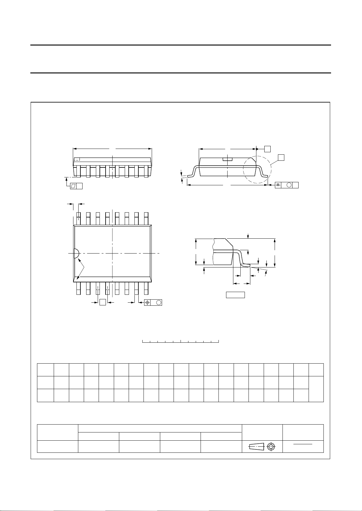
SO16: plastic small outline package; 16 leads; body width 7.5 mm
D
c
y
Z
16
9
TDA9820
SOT162-1
E
H
E
A
X
v M
A
pin 1 index
1
e
DIMENSIONS (inch dimensions are derived from the original mm dimensions)
mm
A
max.
2.65
0.10
A
0.30
0.10
0.012
0.004
1
A2A
2.45
2.25
0.096
0.089
0.25
0.01
b
3
p
0.49
0.36
0.019
0.013
0.014
0.009
UNIT
inches
Note
1. Plastic or metal protrusions of 0.15 mm maximum per side are not included.
8
w M
b
p
0 5 10 mm
scale
(1)E(1) (1)
cD
0.32
10.5
0.23
10.1
0.41
0.40
0.30
0.29
eHELLpQ
7.6
1.27
7.4
0.050
A
2
10.65
10.00
0.42
0.39
A
1
1.4
0.055
1.1
0.4
0.043
0.016
detail X
0.043
0.039
1.1
1.0
Q
3
0.25 0.1
0.01
A
θ
ywv θ
0.004
Z
0.9
0.4
0.035
0.016
o
8
o
0
(A )
L
p
L
0.25
0.01
OUTLINE
VERSION
SOT162-1
1996 Nov 20 14
REFERENCES
IEC JEDEC EIAJ
075E03 MS-013AA
EUROPEAN
PROJECTION
ISSUE DATE
92-11-17
95-01-24

Philips Semiconductors Product specification
Multistandard/dual channel TV FM
intercarrier sound demodulator
SOLDERING
Introduction
There is no soldering method that is ideal for all IC
packages. Wave soldering is often preferred when
through-hole and surface mounted components are mixed
on one printed-circuit board. However, wave soldering is
not always suitable for surface mounted ICs, or for
printed-circuits with high population densities. In these
situations reflow soldering is often used.
This text gives a very brief insight to a complex technology.
A more in-depth account of soldering ICs can be found in
our
“IC Package Databook”
DIP
OLDERING BY DIPPING OR BY WA VE
S
The maximum permissible temperature of the solder is
260 °C; solder at this temperature must not be in contact
with the joint for more than 5 seconds. The total contact
time of successive solder waves must not exceed
5 seconds.
The device may be mounted up to the seating plane, but
the temperature of the plastic body must not exceed the
specified maximum storage temperature (T
printed-circuit board has been pre-heated, forced cooling
may be necessary immediately after soldering to keep the
temperature within the permissible limit.
EPAIRING SOLDERED JOINTS
R
Apply a low voltage soldering iron (less than 24 V) to the
lead(s) of the package, below the seating plane or not
more than 2 mm above it. If the temperature of the
soldering iron bit is less than 300 °C it may remain in
contact for up to 10 seconds. If the bit temperature is
between 300 and 400 °C, contact may be up to 5 seconds.
SO
REFLOW SOLDERING
Reflow soldering techniques are suitable for all SO
packages.
(order code 9398 652 90011).
). If the
stg max
TDA9820
Several techniques exist for reflowing; for example,
thermal conduction by heated belt. Dwell times vary
between 50 and 300 seconds depending on heating
method. Typical reflow temperatures range from
215 to 250 °C.
Preheating is necessary to dry the paste and evaporate
the binding agent. Preheating duration: 45 minutes at
45 °C.
AVE SOLDERING
W
Wave soldering techniques can be used for all SO
packages if the following conditions are observed:
• A double-wave (a turbulent wave with high upward
pressure followed by a smooth laminar wave) soldering
technique should be used.
• The longitudinal axis of the package footprint must be
parallel to the solder flow.
• The package footprint must incorporate solder thieves at
the downstream end.
During placement and before soldering, the package must
be fixed with a droplet of adhesive. The adhesive can be
applied by screen printing, pin transfer or syringe
dispensing. The package can be soldered after the
adhesive is cured.
Maximum permissible solder temperature is 260 °C, and
maximum duration of package immersion in solder is
10 seconds, if cooled to less than 150 °C within
6 seconds. Typical dwell time is 4 seconds at 250 °C.
A mildly-activated flux will eliminate the need for removal
of corrosive residues in most applications.
EPAIRING SOLDERED JOINTS
R
Fix the component by first soldering two diagonally-
opposite end leads. Use only a low voltage soldering iron
(less than 24 V) applied to the flat part of the lead. Contact
time must be limited to 10 seconds at up to 300 °C. When
using a dedicated tool, all other leads can be soldered in
one operation within 2 to 5 seconds between
270 and 320 °C.
Reflow soldering requires solder paste (a suspension of
fine solder particles, flux and binding agent) to be applied
to the printed-circuit board by screen printing, stencilling or
pressure-syringe dispensing before package placement.
1996 Nov 20 15

Philips Semiconductors Product specification
Multistandard/dual channel TV FM
TDA9820
intercarrier sound demodulator
DEFINITIONS
Data sheet status
Objective specification This data sheet contains target or goal specifications for product development.
Preliminary specification This data sheet contains preliminary data; supplementary data may be published later.
Product specification This data sheet contains final product specifications.
Limiting values
Limiting values given are in accordance with the Absolute Maximum Rating System (IEC 134). Stress above one or
more of the limiting values may cause permanent damage to the device. These are stress ratings only and operation
of the device at these or at any other conditions above those given in the Characteristics sections of the specification
is not implied. Exposure to limiting values for extended periods may affect device reliability.
Application information
Where application information is given, it is advisory and does not form part of the specification.
LIFE SUPPORT APPLICATIONS
These products are not designed for use in life support appliances, devices, or systems where malfunction of these
products can reasonably be expected to result in personal injury. Philips customers using or selling these products for
use in such applications do so at their own risk and agree to fully indemnify Philips for any damages resulting from such
improper use or sale.
1996 Nov 20 16
 Loading...