


INTEGRATED CIRCUITS
DATA SH EET
TDA8360; TDA8361; TDA8362
Integrated PAL and PAL/NTSC TV
processors
Objective specification
File under Integrated Circuits, IC02
Philips Semiconductors
September 1995

Philips Semiconductors Objective specification
Integrated PAL and PAL/NTSC TV
processors
FEATURES
Available in TDA8360, TDA8361
and TDA8362
• Vision IF amplifier with high
sensitivity and good differential
gain and phase
• Multistandard FM sound
demodulator (4.5 MHz to 6.5 MHz)
• Integrated chrominance trap and
bandpass filters (automatically
calibrated)
• Integrated luminance delay line
• RGB control circuit with linear RGB
inputs and fast blanking
• Horizontal synchronization with two
control loops and alignment-free
horizontal oscillator without
external components
• Vertical count-down circuit
(50/60 Hz) and vertical preamplifier
• Low dissipation (700 mW)
• Small amount of peripheral
components compared with
competition ICs
• Only one adjustment (vision IF
demodulator)
• The supply voltage for the ICs is
8 V. They are mounted in a shrink
DIL envelope with 52 pins and are
pin compatible.
Additional features
TDA8360
• Alignment-free PAL colour decoder
for all PAL standards, including
PAL-N and PAL-M.
TDA8361
• PAL/NTSC colour decoder with
automatic search system
• Source selection for external
audio/video (A/V) inputs (separate
Y/C signals can also be applied).
TDA8362
• Multistandard vision IF circuit
(positive and negative modulation)
• PAL/NTSC colour decoder with
automatic search system
• Source selection for external
A/V inputs (separate Y/C signals
can also be applied)
• Easy interfacing with the TDA8395
(SECAM decoder) for
multistandard applications.
TDA8360; TDA8361; TDA8362
GENERAL DESCRIPTION
The TDA8360, TDA8361 and
TDA8362 are single-chip TV
processors which contain nearly all
small signal functions that are
required for a colour television
receiver. For a complete receiver the
following circuits need to be added:
a base-band delay line (TDA4661),
a tuner and output stages for audio,
video and horizontal and vertical
deflection.
Because of the different functional
contents of the ICs the set maker can
make the optimum choice depending
on the requirements for the receiver.
The TDA8360 is intended for simple
PAL receivers (all PAL standards,
including PAL-N and PAL-M are
possible).
The TDA8361 contains a PAL/NTSC
decoder and has an A/V switch.
For real multistandard applications
the TDA8362 is available. In addition
to the extra functions which are
available in the TDA8361, the
TDA8362 can handle signals with
positive modulation and it supplies
the signals which are required for the
SECAM decoder TDA8395.
ORDERING INFORMATION
EXTENDED TYPE
NUMBER
TDA8360 52 shrink DIL plastic SOT247AG
TDA8361 52 shrink DIL plastic SOT247AG
TDA8362 52 shrink DIL plastic SOT247AG
September 1995 2
PACKAGE
PINS PIN POSITION MATERIAL CODE
Philips Semiconductors Objective specification
Integrated PAL and PAL/NTSC TV
TDA8360; TDA8361; TDA8362
processors
QUICK REFERENCE DATA
SYMBOL PARAMETER CONDITIONS MIN. TYP. MAX. UNIT
V
P
I
P
Input voltages
V
45,46(rms)
V
5(rms)
V
6(rms)
V
15(p-p)
V
22,23,24(p−p)
Output signals
V
O(p-p)
I
47
V
44
V
50(rms)
V
18,19,20(p-p)
I
37
I
43
Control voltages
V
control
supply voltage 7.2 8.0 8.8 V
supply current − 80 − mA
video IF amplifier sensitivity (RMS value) − 70 100 µV
sound IF amplifier sensitivity (RMS value) − 1 − mV
external audio input (RMS value) TDA8361, TDA8362 − 350 − mV
external CVBS input (peak-to-peak value) TDA8361, TDA8362 − 1 − V
RGB inputs (peak-to-peak value) − 0.7 − V
demodulated CVBS output
− 2.4 − V
(peak-to-peak value)
tuner AGC control current 0 − 5mA
AFC output voltage swing − 6 − V
audio output voltage (RMS value) − 700 − mV
RGB output signal amplitudes
− 4 − V
(peak-to-peak value)
horizontal output current 10 −−mA
vertical output current 1 −−mA
control voltages for Volume, Contrast,
0 − 5V
Saturation, Brightness, Hue and Peaking
September 1995 3
Philips Semiconductors Objective specification
Integrated PAL and PAL/NTSC TV
processors
DET
33
PHASE
DETECTOR
FBI/SCO
flyback sandcastle
PH2LF
PH1LF
XTAL1 XTAL2
HOUT
VSTART
39 38 37 34 3543
36
XTAL
OSCILLATOR
PHASE 2
PHASE 1
KILLERS
COLOUR
TUNING
LINE
OSCILLATOR
to
TDA4661
R-Y output
B-Y output
30
31
DEMODULATOR
PAL
IDENTIFICATION
ACC
AMPLIFIER
DETECTOR
COINCIDENCE
SAT
26
TDA8360; TDA8361; TDA8362
from
TDA4661
B-Y input
R-Y input
28
29
SET
CLAMPS
MATRIX
BANDPASS
CHROMINANCE
RESET
POWER
RIN
222324
BIN
GIN
21
CLAMP
SWITCH
MATRIX
LUMINANCE
Y DELAY
PEAKING
BYPASS
TRAP AND
RGBIN
BOUT
GOUT
181920
OUTPUT
PWL
ROUT
STAGES
MLA621 - 1
17
13 14 25
BRIPEAKIN
CON
INT
CVBS
VRAMP
41 42 40
AGC
DEC
VOUT
ADJ
TUNE
VFB
AGCOUT
49
47 48
VERTICAL
AGC
IF
45
IFIN1
OUTPUT
AMPLIFIER
46
IFIN2
DIVIDER
VERTICAL
AFC AND
SAMPLE-
AND-HOLD
DEMODULATOR
2
3
IFDEM1
44
IFDEM2
AFCOUT
H AND V
SEPARATION
VIDEO
IDENTIFICATION
VIDEO
AMPLIFIER
7
IFOUT
September 1995 4
4
IDENT
TDA8360
12
NOISE
DETECTOR
SUPPLY
TEST
8
DIG
DEC
AUDEEM
1
TUNING
MUTE
PREAMPLIFIER
VOLUME
50
DEM
AUOUT
DEC
PLLLIMITER
910 52
11
51
5
SOIF
P
V
GND2 GND1
control
volume
FT
DEC
BG
DEC
Fig.1 Block diagram for TDA8360.

Philips Semiconductors Objective specification
Integrated PAL and PAL/NTSC TV
processors
sandcastle
FBI/SCO
flayback
PH2LF
PH1LF
XTAL1 XTAL2
HOUT
VSTART
36 39 38 37 34 3543
HUE
27
HUE
CONTROL
XTAL
OSCILLATOR
PHASE 2
PHASE 1
DET
33
PHASE
DETECTOR
KILLERS
COLOUR
TUNING
LINE
OSCILLATOR
R-Y output
to
TDA4661
B-Y output
30
31
DEMODULATOR
SYSTEM
MANAGER
ACC
AMPLIFIER
DETECTOR
COINCIDENCE
SAT
26
TDA8360; TDA8361; TDA8362
from
TDA4661
B-Y input
R-Y input
28
29
SET
CLAMPS
MATRIX
BANDPASS
CHROMINANCE
RESET
POWER
RIN
222324
BIN
GIN
21
CLAMP
SWITCH
MATRIX
LUMINANCE
Y DELAY
PEAKING
BYPASS
TRAP AND
RGBIN
BOUT
181920
ROUT
GOUT
MLA622 - 1
17
STAGES
OUTPUT
PWL
SWITCH
CHROMINANCE
14
15
SWITCH
13 16 25
LUMINANCE
BRI
CON
CHROMA
PEAKIN
EXT
CVBS
INT
CVBS
VRAMP
41 42 40
AGC
DEC
VOUT
ADJ
TUNE
VFB
AGCOUT
49
47 48
VERTICAL
AGC
IF
45
IFIN1
OUTPUT
AMPLIFIER
46
IFIN2
DIVIDER
VERTICAL
AFC AND
SAMPLE-
AND-HOLD
DEMODULATOR
2
3
IFDEM1
44
IFDEM2
AFCOUT
H AND V
SEPARATION
VIDEO
IDENTIFICATION
VIDEO
AMPLIFIER
7
IFOUT
September 1995 5
4
IDENT
TDA8361
12
NOISE
DETECTOR
SUPPLY
TEST
DIG
DEC
1
AUDEEM
8
6
EXTAU
TUNING
MUTE
PREAMPLIFIER
VOLUME
50
51
DEM
AUOUT
DEC
PLLLIMITER
5
910 52
11
SOIF
P
V
GND2 GND1
control
volume
FT
DEC
BG
DEC
Fig.2 Block diagram for TDA8361.
Philips Semiconductors Objective specification
Integrated PAL and PAL/NTSC TV
processors
DET
R-Y output
30
DETECTOR
MANAGER
OSCILLATOR
DIVIDER
sandcastle
FBI/SCO
flyback
PH2LF
PH1LF
VRAMP
XTAL1 XTAL2
VOUT
HUE
XTALOUT
HOUT
VSTART
VFB
36 39 38 37 34 35 32 2743
41 42 40
HUE
CONTROL
XTAL
OSCILLATOR
PHASE 2
PHASE 1
OUTPUT
VERTICAL
33
PHASE
SYSTEM
TUNING
LINE
VERTICAL
to
TDA4661
B-Y output
31
DEMODULATOR
KILLERS
COLOUR
DETECTOR
COINCIDENCE
H AND V
SEPARATION
RESET
POWER
from
TDA4661
B-Y input
28
29
SET
CLAMPS
MATRIX
ACC
AMPLIFIER
NOISE
DETECTOR
TDA8362
TDA8360; TDA8361; TDA8362
BIN
R-Y input
RIN
GIN
222324
CLAMP
SWITCH
MATRIX
LUMINANCE
BANDPASS
CHROMINANCE
SWITCH
CHROMINANCE
BYPASS
TRAP AND
BOUT
GOUT
181920
STAGES
OUTPUT
PWL
Y DELAY
PEAKING
SWITCH
LUMINANCE
TUNING
ROUT
MBC214 - 1
17
16 13 15 14 2526 21
12
BRIPEAKINCVBS
CON
RGBIN
SAT
EXT
INT
CVBS
CHROMA
FT
DEC
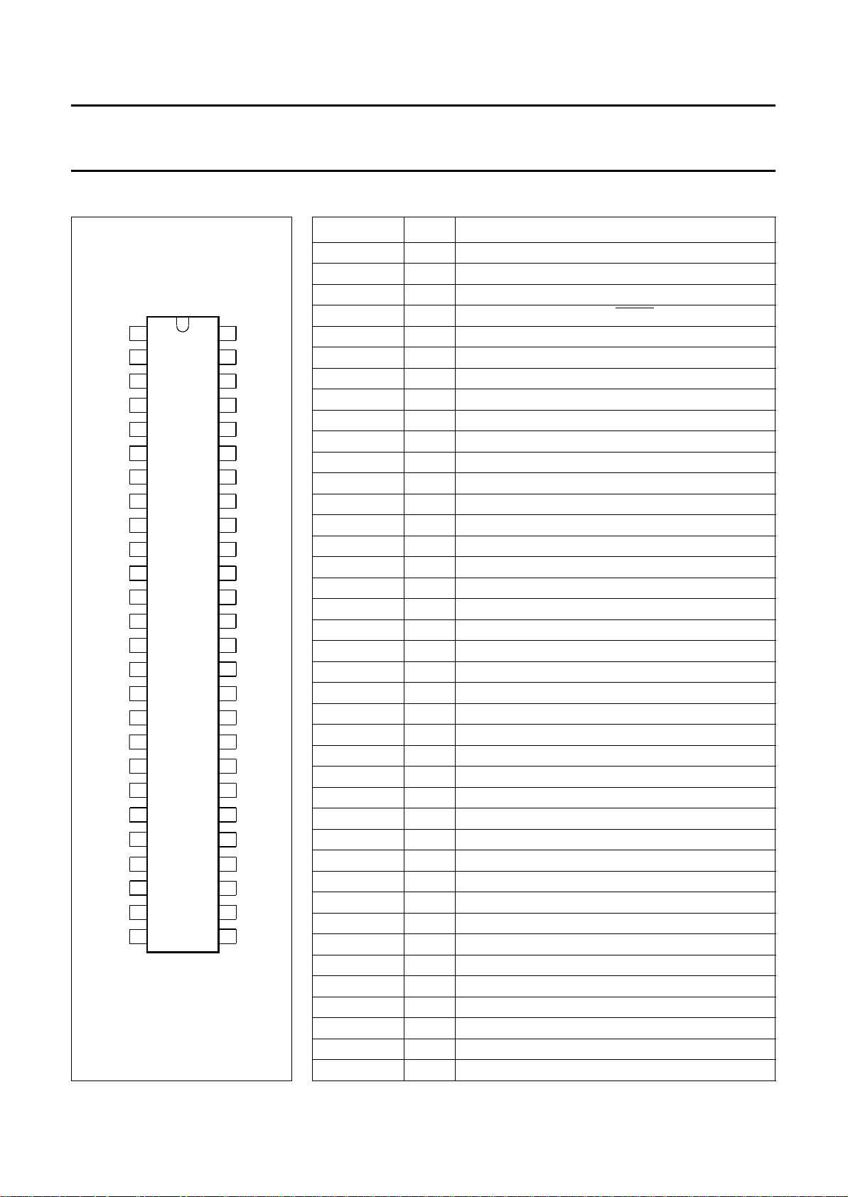
Fig.3 Block diagram for TDA8362.
September 1995 6
AGC
DEC
AUOUT
AFCOUT
AGCOUT
IDENT
DEM
DEC
PLL
LIMITER
5
51
SOIF
control
volume
TEST
SUPPLY
8
DIG
DEC
910 52
11
P
V
GND2 GND1
BG
DEC
AGC
47 48 44
50
4
IF
AMPLIFIER
45
46
IFIN1
IFIN2
49
ADJ
TUNE
AFC AND
SAMPLE-
DEMODULATOR
2
IFDEM1
AND-HOLD
3
7
IFDEM2
IFOUT
VIDEO
AMPLIFIER
VIDEO
IDENTIFICATION
1
MUTE
PREAMPLIFIER
SWITCH
VOLUME
6
AUDEEM
EXTAU
Philips Semiconductors Objective specification
Integrated PAL and PAL/NTSC TV
processors
PINNING (TDA8362)
SYMBOL PIN DESCRIPTION
AUDEEM 1 audio de-emphasis and ± modulation switch
IFDEM1 2 IF demodulator tuned circuit
IFDEM2 3 IF demodulator tuned circuit
IDENT 4 video identification output/
52
51
50
49
48
47
46
45
44
43
42
41
40
39
38
37
36
35
34
33
32
31
30
29
28
27
DEC
BG
DEC
DEM
AUOUT
TUNE
ADJ
DEC
AGC
AGCOUT
IFIN2
IFIN1
AFCOUT
VOUT
VRAMP
VFB
PH1LF
PH2LF
FBI/SCO
HOUT
VSTART
XTAL2
XTAL1
DET
XTALOUT
BYO
RYO
RYI
BYI
HUE
SOIF 5 sound IF input and volume control
EXTAU 6 external audio input
IFOUT 7 IF video output
DEC
DIG
GND1 9 ground 1
V
P
GND2 11 ground 2
DEC
FT
CVBS
PEAKIN 14 peaking control input
CVBS
CHROMA 16 chrominance and A/V switch input
BRI 17 brightness control input
BOUT 18 blue output
GOUT 19 green output
ROUT 20 red output
RGBIN 21 RGB insertion and blanking input
RIN 22 red input
GIN 23 green input
BIN 24 blue input
CON 25 contrast control input
SAT 26 saturation control input
HUE 27 hue control input (or chrominance output)
BYI 28 B−Y input signal
RYI 29 R−Y input signal
RYO 30 R−Y output signal
BYO 31 B−Y output signal
XTALOUT 32 4.43 MHz output for TDA8395
DET 33 loop filter burst phase detector
XTAL1 34 3.58 MHz crystal connection
XTAL2 35 4.43 MHz crystal connection
VSTART 36 supply/start horizontal oscillator
HOUT 37 horizontal output
FBI/SCO 38 flyback input/sandcastle output
PH2LF 39 phase 2 loop filter
PH1LF 40 phase 1 loop filter
IDENT
SOIF
IFOUT
DIG
GND1
V
GND2
FT
INT
EXT
BRI
BOUT
GOUT
ROUT
RIN
GIN
BIN
CON
SAT
1
2
3
4
5
6
7
8
9
10
P
11
12
13
TDA8362
14
15
16
17
18
19
20
21
22
23
24
25
26
MBC203
AUDEEM
IFDEM1
IFDEM2
EXTAU
DEC
DEC
CVBS
PEAKIN
CVBS
CHROMA
RGBIN
Fig.4 Pin configuration for
TDA8362.
INT
EXT
TDA8360; TDA8361; TDA8362
MUTE input
8 decoupling digital supply
10 supply voltage (+8 V)
12 decoupling filter tuning
13 internal CVBS input
15 external CVBS input
September 1995 7

Philips Semiconductors Objective specification
Integrated PAL and PAL/NTSC TV
processors
SYMBOL PIN DESCRIPTION
VFB 41 vertical feedback input
VRAMP 42 vertical ramp generator
VOUT 43 vertical output
AFCOUT 44 AFC output
IFIN1 45 IF input 1
IFIN2 46 IF input 2
AGCOUT 47 tuner AGC output
DEC
AGC
TUNE
ADJ
AUOUT 50 audio output
DEC
DEM
DEC
BG
TDA8360
The TDA8360 has the following
differences to the pinning:
Pin 6: external audio input not
connected
Pin 15: external CVBS input not
connected
Pin 16: chrominance and A/V switch
input not connected
Pin 27: hue control input not
connected.
TDA8361
The TDA8361 has the following
differences to the pinning:
Pin 1: only audio de-emphasis
Pin 27: only hue control
Pin 32: 4.43 MHz output for TDA8395
is not connected.
FUNCTIONAL DESCRIPTION
Video IF amplifier
The IF amplifier contains
3 AC-coupled control stages with a
total gain control range of greater
than 60 dB. The sensitivity of the
circuit is comparable with that of
modern IF ICs.
48 AGC decoupling capacitor
49 tuner take-over adjustment
51 decoupling sound demodulator
52 decoupling bandgap supply
The reference carrier for the video
demodulator is obtained by means of
passive regeneration of the picture
carrier. The external reference tuned
circuit is the only remaining
adjustment of the IC.
In the TDA8362 the polarity of the
demodulator can be switched so that
the circuit is suitable for both positive
and negative modulated signals.
The AFC circuit is driven with the
same reference signal as the video
demodulator. To ensure that the
video content does not disturb the
AFC operation a sample-and-hold
circuit is incorporated; the capacitor
for this function is internal. The AFC
output voltage is 6 V.
The AGC detector operates on levels,
top sync for negative modulated and
top white for positive modulated
signals.The AGC detector time
constant capacitor is connected
externally. This is mainly because of
the flexibility of the application.
The time constant of the AGC system
during positive modulation
(TDA8362) is slow, this is to avoid any
visible picture variations. This,
however, causes the system to react
very slowly to sudden changes in the
input signal amplitude.
TDA8360; TDA8361; TDA8362
To overcome this problem a speed-up
circuit has been included which
detects whether the AGC detector is
activated every frame period. If,
during a 3-frame period, no action is
detected the speed of the system is
increased. When the incoming signal
has no peak white information (e.g.
test lines in the vertical retrace period)
the gain would be video signal
dependent. To avoid this effect the
circuit also contains a black level
AGC detector which is activated when
the black level of the video signal
exceeds a certain level.
The TDA8361 and TDA8362 contain
a video identification circuit which is
independent of the synchronization
circuit. Therefore search tuning is
possible when the display section of
the receiver is used as a monitor. In
the TDA8360 this circuit is only used
for stable OSD at no signal input. In
the normal television mode the
identification output is connected to
the coincidence detector, this applies
to all three devices. The identification
output voltage is LOW when no
transmitter is identified. In this
condition the sound demodulator is
switched off (mute function). When a
transmitter is identified the output
voltage is HIGH. The voltage level is
dependent on the frequency of the
incoming chrominance signal.
September 1995 8

Philips Semiconductors Objective specification
Integrated PAL and PAL/NTSC TV
processors
Sound circuit
The sound bandpass and trap filters
have to be connected externally. The
filtered intercarrier signal is fed to a
limiter circuit and is demodulated by
means of a PLL demodulator. The
PLL circuit tunes itself automatically
to the incoming signal, consequently,
no adjustment is required.
The volume is DC controlled. The
composite audio output signal has an
amplitude of 700 mV RMS at a
volume control setting of −6 dB. The
de-emphasis capacitor has to be
connected externally. The
non-controlled audio signal can be
obtained from this pin via a buffer
stage. The amplitude of this signal is
350 mV RMS.
The TDA8361 and TDA8362 external
audio input signal must have an
amplitude of 350 mV RMS. The
audio/video switch is controlled via
the chrominance input pin.
Synchronization circuit
The sync separator is preceded by a
voltage controlled amplifier which
adjusts the sync pulse amplitude to a
fixed level. The sync pulses are then
fed to the slicing stage (separator)
which operates at 50% of the
amplitude.
The separated sync pulses are fed to
the first phase detector and to the
coincidence detector. The
coincidence detector is used for
transmitter identification and to detect
whether the line oscillator is
synchronized. When the circuit is not
synchronized the voltage on the
peaking control pin (pin 14) is LOW
so that this condition can be detected
externally. The first PLL has a very
high static steepness, this ensures
that the phase of the picture is
independent of the line frequency.
The line oscillator operates at twice
the line frequency.
The oscillator network is internal.
Because of the spread of internal
components an automatic adjustment
circuit has been added to the IC.
The circuit compares the oscillator
frequency with that of the crystal
oscillator in the colour decoder. This
results in a free-running frequency
which deviates less than 2% from the
typical value.
The circuit employs a second control
loop to generate the drive pulses for
the horizontal driver stage.
X-ray protection can be realised by
switching the pin of the second
control loop to the positive supply line.
The detection circuit must be
connected externally. When the X-ray
protection is active the horizontal
output voltage is switched to a high
level. When the voltage on this pin
returns to its normal level the
horizontal output is released again.
The IC contains a start-up circuit for
the horizontal oscillator. When this
feature is required a current of 6.5 mA
has to be supplied to pin 36. For an
application without start-up both
supply pins (10 and 36) must be
connected to the 8 V supply line.
The drive signal for the vertical ramp
generator is generated by means of a
divider circuit. The RC network for the
ramp generator is external.
Integrated video filters
The circuit contains a chrominance
bandpass and trap circuit. The filters
are realised by means of gyrator
circuits and are automatically tuned
by comparing the tuning frequency
with the crystal frequency of the
decoder.
In the TDA8361 and TDA8362 the
chrominance trap is active only when
the separate chrominance input pin is
connected to ground or to the positive
supply voltage and when a colour
signal is recognized.
TDA8360; TDA8361; TDA8362
When the pin is left open-circuit the
trap is switched off so that the circuit
can also be used for S-VHS
applications.
The luminance delay line and the
delay for the peaking circuit are also
realised by means of gyrator circuits.
Colour decoder
The colour decoder in the various ICs
contains an alignment-free crystal
oscillator, a colour killer circuit and
colour difference demodulators.
The 90° phase shift for the reference
signal is achieved internally. Because
the main differences of the 3 ICs are
found in the colour decoder the
various types will be discussed.
TDA8360
This IC contains only a PAL decoder.
Depending on the frequency of the
crystals which are connected to the IC
the decoder can demodulate all PAL
standards. Because the horizontal
oscillator is calibrated by using the
crystal frequency as a reference the
4.4 MHz crystal must be connected to
pin 35 and the 3.5 MHz crystal to
pin 34. When only one crystal is
connected to the IC the other crystal
pin must be connected to the positive
supply rail via a 47 kΩ resistor. For
applications with two 3.5 MHz
crystals both must be connected to
pin 34 and the switching between the
crystals must be made externally.
Switching of the crystals is only
allowed directly after the vertical
retrace. The circuit will indicate
whether a PAL signal has been
identified by the colour decoder via
the saturation control pin.
When two crystals are connected to
the IC the output voltage of the video
identification circuit indicates the
frequency of the incoming
chrominance signal.
September 1995 9

Philips Semiconductors Objective specification
Integrated PAL and PAL/NTSC TV
processors
The conditions are:
• Signal identified at
f
= 3.6 MHz; VO = 6 V
osc
• Signal identified at
f
= 4.4 MHz (or no colour);
osc
VO = 8 V.
This information can be used to
switch the sound bandpass filter and
trap filter.
TDA8361
This IC contains an automatic
PAL/NTSC decoder. The conditions
for connecting the reference crystals
are the same as for the TDA8360.
The decoder can be forced to PAL
when the hue control pin is connected
to the positive supply voltage via a
5kΩ or 10 kΩ resistor
(approximately). The decoder cannot
be forced to the NTSC standard. It is
also possible to see if a colour signal
is recognized via the saturation pin.
TDA8362
In addition to the possibilities of the
TDA8361, the TDA8362 can
co-operate with the SECAM add-on
decoder TDA8395.
The communication between the two
ICs is achieved via pin 32. The
TDA8362 supplies the reference
signal (4.43 MHz) for the calibration
system of the TDA8395, identification
of the colour standard is via the same
connection. When a SECAM signal is
detected by the TDA8395 the IC will
draw a current of 150 µA. When
TDA8362 has not identified a colour
signal in this condition it will go into
the SECAM mode, that means it will
switch off the R−Y and B−Y outputs
and increase the voltage level on
pin 32.
This voltage will switch off the
colour-killer in the TDA8395 and
switch on the R−Y and B−Y outputs of
the TDA8395. Forcing the system to
the SECAM standard can be
achieved by loading pin 32 with a
current of 150 µA. Then the system
manager in the TDA8362 will not
search for PAL or NTSC signals.
Forcing to NTSC is not possible.
For PAL/SECAM applications the
input signal for the TDA8395 can be
obtained from pin 27 (hue control)
when this pin is connected to the
positive supply rail via the 5 kΩ or
10 kΩ resistor. An external source
selector is required by the
TDA8395/TDA8362 combination for
PAL/SECAM/NTSC applications.
RGB output circuit
The colour difference signals are
matrixed with the luminance signal to
obtain the RGB signals. Linear
amplifiers have been chosen for the
RGB inputs so that the circuit is
suitable for incoming signals from the
SCART connector. The contrast and
brightness controls operate on
internal and external signals.
The fast blanking pin has a second
detection level at 3.5 V.
When this level is exceeded the
RGB outputs are blanked so that
“On-Screen-Display” signals can be
applied to the outputs.
The output signal has an amplitude of
approximately 4 V, black-to-white,
with nominal input signals and
nominal control settings. The nominal
black level is 1.3 V.
TDA8360; TDA8361; TDA8362
September 1995 10

Philips Semiconductors Objective specification
Integrated PAL and PAL/NTSC TV
TDA8360; TDA8361; TDA8362
processors
LIMITING VALUES
In accordance with the Absolute Maximum Rating System (IEC134).
SYMBOL PARAMETER MIN. MAX. UNIT
V
P
T
stg
T
amb
T
sol
T
j
THERMAL RESISTANCE
SYMBOL PARAMETER THERMAL RESISTANCE
R
th j-a
CHARACTERISTICS
V
= 8 V; T
P
SYMBOL PARAMETER CONDITIONS MIN. TYP. MAX. UNIT
supply voltage − 9.0 V
storage temperature −25 +150 °C
operating ambient temperature −25 +70 °C
soldering temperature for 5 s − 260 °C
maximum junction temperature (operating) − 150 °C
from junction to ambient in free air 40 K/W
= 25 °C; unless otherwise specified.
amb
Supplies
V
P
I
P
I
HOSC
supply voltage (pin 10) 7.2 8.0 8.8 V
supply current (pin 10) − 80 − mA
horizontal oscillator start current
(pin 36)
P
tot
total power dissipation including start supply − 0.7 − W
IF circuit
ISION IF AMPLIFIER INPUTS (PINS 45 AND 46)
V
V
R
C
G
V
i(rms)
I
I
cr
i(rms)
input sensitivity (RMS value) note 2
Input resistance (differential) note 3 − 2 − kΩ
Input capacitance (differential) note 3 − 3 − pF
gain control range 64 −−dB
maximum input signal (RMS value) 100 −−mV
note 1 6.5 −−mA
= 38.90 MHz − 70 100 µV
f
i
= 45.75 MHz − 70 100 µV
f
i
= 58.75 MHz − 70 100 µV
f
i
September 1995 11

Philips Semiconductors Objective specification
Integrated PAL and PAL/NTSC TV
TDA8360; TDA8361; TDA8362
processors
SYMBOL PARAMETER CONDITIONS MIN. TYP. MAX. UNIT
VIDEO AMPLIFIER OUTPUT; NOTE 4(PIN 7)
V
7
V
7
∆V
7
V
7
Z
O
I
bias
I
source
B bandwidth of demodulated output
G
diff
Φ
diff
NL
vid
V
th
V
ins
N
clamp
N
ins
δ
mod
S/N signal-to-noise ratio notes 7 and 11
V
7
V
7
negative modulation
zero signal output level note5 4.45 4.6 4.75 V
top sync level 1.9 2 2.1 V
positive modulation (TDA8362)
zero signal output level note5 1.85 2 2.15 V
white level 4.2 4.3 4.4 V
difference in amplitude between
− 015%
negative and positive modulation
detection level of black level for
− 3.1 − V
positive modulation when no peak
white is available in the signal
video output impedance −−50 Ω
internal bias current of NPN emitter
1 −−mA
follower output transistor
maximum source current −−5mA
−3dB 6 9 − MHz
signal
gain differential note 6 − 25%
phase differential notes 6 and 7 − 1 5 deg
video non linearity note 8 −−5%
white spot threshold voltage level − 4.8 − V
white spot insertion voltage level − 3.2 − V
noise inverter clamping voltage level − 1.4 − V
noise inverter insertion level note 9 − 2.6 − V
intermodulation notes 7 and 10
blue V
yellow V
blue V
yellow V
= 0.92 or 1.1 MHz 60 66 − dB
o
= 0.92 or 1.1 MHz 56 62 − dB
o
= 2.66 or 3.3 MHz 60 66 − dB
o
= 2.66 or 3.3 MHz 60 66 − dB
o
Vi = 10 mV 52 60 − dB
end of control range 52 61 − dB
residual carrier signal note 7 − 1 − mV
residual 2nd harmonic of carrier
note 7 − 0.5 − mV
signal
September 1995 12

Philips Semiconductors Objective specification
Integrated PAL and PAL/NTSC TV
TDA8360; TDA8361; TDA8362
processors
SYMBOL PARAMETER CONDITIONS MIN. TYP. MAX. UNIT
IF AND TUNER AGC; NOTE 12
Timing of IF-AGC (C48 = 2.2µF)
modulated video interference 30% AM for 1 to
100 mV; 0 to 200 Hz
t
inc
response time for an IF input signal
amplitude increase of 52 dB for
positive and negative modulation
t
dec
response time for an IF input signal
amplitude decrease of 52 dB
for negative modulation − 25 − ms
for positive modulation (TDA8362) − 100 − ms
I
leak
allowed leakage current of the AGC
note 13
capacitor
for negative modulation −−10 µA
for positive modulation −−200 nA
Tuner take-over adjustment (pin 49)
V
49(rms)
minimum starting level voltage for
tuner take-over (RMS value)
V
49(rms)
maximum starting level voltage for
tuner take-over (RMS value)
V
cr
control voltage range 0.5 − 4.5 V
Tuner control output (pin 47)
V
47
V
47(sat)
maximum tuner AGC output voltage maximum gain −−V
output saturation voltage minimum gain;
I47=2mA
I
47
I
leak
∆V
47
maximum tuner AGC output swing 5 −−mA
leakage current RF AGC −−1µA
input signal variation for complete
I
= 1 mA 1 2 4 dB
O(max)
tuner control
AFC OUTPUT; NOTE 14 (PIN 44)
V
44
f
sl
f
os
V
O
Z
O
output voltage swing − 6 − V
AFC slope − 33 − mV/kHz
AFC offset note 7 −−50 kHz
output voltage at centre frequency − 3.5 − V
output impedance − 50 − kΩ
SWITCHING TO POSITIVE MODULATION (TDA8362);NOTE 15(PIN 1)
V
1
minimum voltage on pin 1 to switch
the video demodulator and AGC to
positive modulation
I
I
input current −−1mA
−−10 %
− 2 − ms
− 0.2 0.5 mV
100 150 − mV
+ 1 V
P
−−300 mV
−−V
−1V
P
September 1995 13

Philips Semiconductors Objective specification
Integrated PAL and PAL/NTSC TV
TDA8360; TDA8361; TDA8362
processors
SYMBOL PARAMETER CONDITIONS MIN. TYP. MAX. UNIT
VIDEO IDENTIFICATION OUTPUT (PIN 4)
V
O
Z
O
V
O
t
d
I
4
Sound circuit
output voltage video not identified −−0.5 V
output impedance − 25 − kΩ
output voltage video identified;
− 6 − V
colour signal
available;
f
= 3.5 MHz
osc
video identified;
− 8 − V
colour signal
available/unavailable
= 4.4 MHz
;f
osc
delay time of identification after
−−10 ms
the AGC has stabilized on a new
transmitter
maximum load current at pin 4 −−25 µA
D
EMODULATOR INPUT; NOTE 16 (PIN 5)
V
5(rms)
input limiting for PLL catching range
− 12mV
(RMS value)
∆f catching range PLL note 17 4.2 − 6.8 MHz
R
I
C
I
AMR AM rejection V
DC input resistance note 3 100 −−kΩ
input capacitance note 3 − 15 − pF
= 50 mV RMS;
I
60 66 − dB
note 18
DE-EMPHASIS (PIN 1)
V
O(rms)
R
O
V
1
output signal amplitude (RMS value) note 17 − 350 − mV
output resistance − 15 − kΩ
DC output voltage − 3 − V
AUDIO ATTENUATOR OUTPUT (PIN 50)
V
50(rms)
controlled output signal amplitude
−6 dB; note 17 500 700 900 mV
(RMS value)
R
O
V
50
output resistance − 250 −Ω
DC output voltage − 3.3 − V
THD total harmonic distortion note 19 −−0.5 %
S/N
int
S/N
ext
VOL
cr
OSS suppression of output signal when
internal signal-to-noise ratio note 7 − 60 − dB
external signal-to-noise ratio note 7 − 80 − dB
control range see also Fig.5 − 80 − dB
− 80 − dB
mute is active
∆V
50
DC shift of the output when mute is
note 20 − 10 50 mV
active
September 1995 14

Philips Semiconductors Objective specification
Integrated PAL and PAL/NTSC TV
TDA8360; TDA8361; TDA8362
processors
SYMBOL PARAMETER CONDITIONS MIN. TYP. MAX. UNIT
EXTERNAL AUDIO INPUT (TDA8361, TDA8362); NOTE 21 (PIN 6)
V
6(rms)
R
I
∆G
V
α
cr
CVBS/On-Screen Display and CD inputs
NTERNAL AND EXTERNAL CVBS INPUTS (PINS 13 AND 15)
I
V
13(p-p)
I
13
V
15(p-p)
I
15
ISS suppression of non-selected CVBS
C
OMBINED CHROMINANCE AND SWITCH INPUT (TDA8361, TDA8362; PIN 16)
V
16(p-p)
V
16(p-p)
R
I
C
I
V
16
V
16
V
16
SS
CVBS
input signal amplitude (RMS value) − 350 700 mV
input resistance − 25 − kΩ
voltage gain difference between input
maximum volume − 12 − dB
and output
crosstalk between internal and
60 −−dB
external audio signals
internal CVBS input voltage
notes 3 and 22 − 2 2.8 V
(peak-to-peak value)
internal CVBS input current − 4 −µA
external CVBS input voltage;
note 3 − 1 1.4 V
TDA8361, TDA8362
(peak-to-peak value)
external CVBS input current;
− 4 −µA
TDA8361, TDA8362
note 23 50 −−dB
input signal; TDA8361, TDA8362
chrominance input voltage
notes 3 and 24 − 0.3 − V
(peak-to-peak value)
input signal amplitude before clipping
note 7 1 −−V
occurs (peak-to-peak value)
chrominance input resistance − 15 − kΩ
chrominance input capacitance note 3 −−5pF
DC input voltage to switch the
−−0.5 V
A/V switch to internal mode
DC input voltage to switch the
VP − 0.5 −−V
A/V switch to external mode
DC input voltage for chrominance
345V
insertion
suppression of non-selected
notes 7 and 23 50 −−dB
chrominance signal from CVBS input
September 1995 15

Philips Semiconductors Objective specification
Integrated PAL and PAL/NTSC TV
TDA8360; TDA8361; TDA8362
processors
SYMBOL PARAMETER CONDITIONS MIN. TYP. MAX. UNIT
RGB INPUTS FOR ON-SCREEN DISPLAY (PINS 22, 23 AND 24)
V
22,23,24(p-p)
input signal amplitude for an output
signal of 4V (black-to-white)
(peak-to-peak value)
V
22,23,24(p-p)
input signal amplitude before clipping
occurs (peak-to-peak value)
V
diff
difference of black level of internal
and external signals at the outputs
I
22,23,24
input currents − 0.1 −µA
FAST BLANKING (PIN 21)
V
I
V
I
V
21(max)
t
d
I
21
SS
int
fast blanking input voltage no data insertion −−0.4 V
fast blanking input voltage data insertion 0.9 −−V
maximum input pulse data insertion −−3V
delay of data insertion −−20 ns
input current − 0.2 − mA
suppression of internal RGB signals
with data insertion at
f = 0 to 5 MHz
SS
ext
suppression of external RGB signals
with data insertion at
f = 0 to 5 MHz
V
I
input voltage to blank the RGB
outputs to facilitate
‘On-Screen-Display’ signals being
applied to these outputs
t
d
delay between the input pulse and
the blanking at the output
COLOUR DIFFERENCE INPUT SIGNALS (PINS 28 AND 29)
V
29(p-p)
input signal amplitude (R−Y)
(peak-to-peak value)
V
28(p-p)
input signal amplitude (B−Y)
(peak-to-peak value)
I
28,29
input current for both inputs − 0.1 1.0 µA
Chrominance filters
note 25 − 0.7 0.8 V
1 −−V
−−100 mV
note 23 46 −−dB
note 23 46 −−dB
note 26 4 −−V
note 7 − 30 − ns
− 1.05 − V
− 1.35 − V
C
HROMINANCE TRAP CIRCUIT
f
trap
trap frequency − f
QF trap quality factor notes 7 and 27 − 2 −
SR colour subcarrier rejection 20 −−dB
CHROMINANCE BANDPASS CIRCUIT
f
c
centre frequency − f
QBP bandpass quality factor note 7 − 3 −
September 1995 16
SC
SC
− MHz
− MHz

Philips Semiconductors Objective specification
Integrated PAL and PAL/NTSC TV
TDA8360; TDA8361; TDA8362
processors
SYMBOL PARAMETER CONDITIONS MIN. TYP. MAX. UNIT
Delay line and peaking circuit
Y DELAY LINE
t
d
B bandwidth of internal delay line note 7 8 −−MHz
PEAKING CONTROL; NOTE 28, SEE ALSO FIG.6 (PIN 14)
t
W
S
cth
I
14
V
I
Horizontal and vertical synchronization circuits
YNC VIDEO INPUT (TDA8361, TDA8362; PINS 13 AND 15)
S
V
13
SL slicing level note 29 − 50 − %
VERTICAL SYNC
t
W
HORIZONTAL OSCILLATOR
f
fr
∆f
fr
/∆V
∆f
osc
P
/∆T frequency variation with temperature T
∆f
osc
∆f
osc( max
FIRST CONTROL LOOP; NOTE 31 (FILTER CONNECTED TO PIN 40)
f
HR
f
CR
S/N signal-to-noise ratio of the video input
HYS hysteresis at the switching point − 3 − dB
delay time note 7 − 480 − ns
width of preshoot or overshoot at 50% of pulse;
− 160 − ns
note 7
peaking signal compression
− 50 − IRE
threshold
input current when no video input
− 1 − mA
signal present
voltage level to switch off peaking − 7 − V
sync pulse amplitude referenced to pin 15;
50 300 − mV
note 3
width of the vertical sync pulse
note 30 22 −−µs
without sync instability
free running frequency note 44 − 15625 − Hz
spread on free running frequency −−±2%
frequency variation with respect to
the supply voltage
VP = 8 V ±10%;
note 7
= 25 °C ±50 °C;
amb
− 0.2 0.5 %
− 1 − Hz/K
note 7
) maximum frequency deviation at the
−−75 %
start of the horizontal output
holding range PLL −±0.9 ±1.2 kHz
catching range PLL note 7 ±0.6 ±0.9 − kHz
− 20 − dB
signal at which the time constant is
switched
September 1995 17

Philips Semiconductors Objective specification
Integrated PAL and PAL/NTSC TV
TDA8360; TDA8361; TDA8362
processors
SYMBOL PARAMETER CONDITIONS MIN. TYP. MAX. UNIT
SECOND CONTROL LOOP; NOTE 32 (CAPACITOR CONNECTED TO PIN 39)
/∆ϕ
∆ϕ
i
o
t
cr
t
shift
/∆ϕ
∆ϕ
i
o
V
39
I
I
HORIZONTAL OUTPUT (PIN 37)
V
OL
I
O(max)
V
O(max)
δ
df
FLYBACK INPUT/SANDCASTLE OUTPUT (PIN 38)
I
38
V
O
V
O
V
Icl
t
W
t
W
t
d
VERTICAL SECTION; NOTE 34
f
fr
f
lock
ERTICAL RAMP GENERATOR (PIN 42)
V
I
42
I
dis
V
saw(p-p)
t
d
control sensitivity without RL on pin 39 − 150 −µs/µs
control range from start of horizontal
11 12 −µs
output to flyback
maximum horizontal shift range note 7 ±2 −−µs
shift control sensitivity note 7 − 3 −µA/µs
voltage to switch on the X-ray
6 −−V
protection
input current during protection −−tbf µA
LOW level output voltage IO = 10 mA −−0.3 V
maximum allowed output current 10 −−mA
maximum allowed output voltage −−V
P
V
duty factor note 7 − 50 − %
required input current during flyback
note 7 100 − 300 µA
pulse
output voltage during burst key 4.8 5.3 5.8 V
output voltage during blanking 1.8 2.0 2.2 V
clamped input voltage during flyback 2.6 3.0 3.4 V
burst key pulse width 3.3 3.5 3.7 µs
vertical blanking pulse width note 33 − 14 − lines
delay of start of burst key to start
5.2 5.4 5.6 µs
of sync
free running frequency − 50/60 − Hz
locking range 45 − 64.5 Hz
divider value not locked − 625/525 −
locking range (lines/frame) 488 − 722
input current during scan note 7 −−2µA
discharge current during retrace − 0.3 − mA
sawtooth amplitude
in 50 Hz mode − 1.5 1.8 V
(peak-to-peak value)
delay from field-to-field −−1.6 µs
September 1995 18

Philips Semiconductors Objective specification
Integrated PAL and PAL/NTSC TV
TDA8360; TDA8361; TDA8362
processors
SYMBOL PARAMETER CONDITIONS MIN. TYP. MAX. UNIT
VERTICAL OUTPUT (PIN 43)
I
O
I
int
V
O(max)
V
O(min)
VERTICAL FEEDBACK INPUT (PIN 41)
V
41
V
41
I
41
∆t
p
∆T/∆V temperature dependency on
VGLvertical guard switching level with
V
GH
t
d
Colour demodulation part
available output current note 7 1 −−mA
internal bias current of NPN emitter
− 0.2 − mA
follower
maximum available output voltage 4 −−V
minimum available output voltage −−0.3 V
DC input voltage 2.0 2.5 3.0 V
AC input voltage − 1 − V
input current −−15 µA
internal pre-correction to sawtooth note 35 − 3 − %
∆T = 40 °C −−1%
amplitude
−−−1.5 V
respect to the DC feedback level;
switching level LOW
vertical guard switching level with
−−+1.5 V
respect to the DC feedback level;
switching level HIGH
delay of scan start power on at 60 Hz − 140 − ms
C
HROMINANCE AMPLIFIER
ACC
cr
ACC control range note 36 26 −−dB
∆V change in amplitude of the output
signals over the ACC range
THR
HYS
on
off
threshold colour killer ON −30 −−38 dB
hysteresis colour killer OFF note 7
strong input signal S/N ≥ 40 dB − +3 − dB
noisy input signal − +1 − dB
CIRCUIT
ACL
chrominance burst ratio at which the
ACL starts to operate
REFERENCE PART
Phase-locked loop; note 37
f
CR
catching range 300 −−Hz
∆ϕ phase shift for a ±200 Hz deviation of
the oscillator frequency
−−2dB
2.3 − 2.7
note 7 −−2 deg
September 1995 19

Philips Semiconductors Objective specification
Integrated PAL and PAL/NTSC TV
TDA8360; TDA8361; TDA8362
processors
SYMBOL PARAMETER CONDITIONS MIN. TYP. MAX. UNIT
Oscillator
TC
osc
∆f
osc
R
I
R
I
C
I
R required resistance to V
HUE CONTROL AND CHROMINANCE OUTPUT (TDA8361, TDA8362); NOTE 38 (PIN 27)
HUE
cr
∆HUE hue variation for ±10% V
∆HUE/∆T hue variation with temperature T
R value of resistor connected to V
V
O(p-p)
DEMODULAT ORS
V
30(p-p)
V
31(p-p)
G gain ratio of both demodulators
Z
O
B bandwidth of demodulators −3 dB; note 40 − 650 − kHz
V
30,31(p-p)
V
30,31(p-p)
temperature coefficient of f
f
deviation with respect to V
osc
osc
P
note 7 − 2.0 2.5 Hz/K
note 7;
−−250 Hz
VP = 8 V ±10%
input resistance (pin 34) fi= 3.58 MHz; note 4 − 1.5 − kΩ
input resistance (pin 35) fi= 4.43 MHz; note 4 − 1 − kΩ
input capacitance (pins 34 and 35) note 4 −−10 pF
to force the
P
− 47 − kΩ
oscillator into one crystal mode
hue control range see also Fig.7 ±45 ±60 − deg
P
note 7 − 0 5 deg
= 0 to +7 °C;
amb
− 0 − deg
note 7
to
P
4.7 10 12 kΩ
switch the P AL decoder and to obtain
a chrominance input signal for the
TDA8395 (TDA8362)
chrominance output signal to the
nominal output signal − 330 − mV
TDA8395 (peak-to-peak value)
(R−Y) output signal amplitude
note 39 − 0.525 − V
(peak-to-peak value)
(B−Y) output signal amplitude
note 39 − 0.675 − V
(peak-to-peak value)
1.6 1.78 1.96
G(B−Y)/G(R−Y)
spread of signal amplitude ratio
note 7 −1 − +1 dB
PAL/NTSC
output impedance (R−Y)/(B−Y)
− 250 −Ω
output
residual carrier output voltage
f = f
osc
(peak-to-peak value)
(R−Y) output −−10 mV
(B−Y) output −−10 mV
residual carrier output voltage
f = 2f
osc
(peak-to-peak value)
(R−Y) output −−10 mV
(B−Y) output −−10 mV
September 1995 20

Philips Semiconductors Objective specification
Integrated PAL and PAL/NTSC TV
TDA8360; TDA8361; TDA8362
processors
SYMBOL PARAMETER CONDITIONS MIN. TYP. MAX. UNIT
DEMODULATORS
V
30(p-p)
/∆T change of output signal amplitude
∆V
O
/∆V
∆V
O
P
ϕ
e
COLOUR DIFFERENCE MATRIXES IN CONTROL CIRCUIT
G−Y/−(R−Y) PAL/SECAM mode with
G−Y/−(B−Y) −−0.19
−(B−Y) NTSC mode; the CD matrix results in
−(R−Y) NTSC mode; the CD matrix results in
G−Y NTSC mode; the CD matrix results in
REFERENCE SIGNAL OUTPUT FOR TDA8395 (TDA8362; PIN 32)
f
ref
V
32(p-p)
V
O
V
O
I
32
H/2 ripple at (R−Y) output
(peak-to-peak value)
only burst fed to
input
−−25 mV
note 7 − 0.1 − %/K
with temperature
change of output signal amplitude
note 7 −−±0.1 dB
with supply voltage
phase error in the demodulated
−−5 deg
signals
TDA8362/TDA8395
−(R−Y) and −(B−Y)
not affected
−−0.51
±10%
−
−
±25%
nominal hue setting −1.12U
− 1.12V
R
R
the following signal (1.14/−10°)
nominal hue setting −0.20UR + 1.12V
R
the following signal (1.14/100°)
nominal hue setting −0.25VR− 0.17U
R
the following signal (0.30/235°)
reference frequency note 41 − 4.43 − MHz
output signal amplitude
0.2 0.25 0.3 V
(peak-to-peak value)
output voltage level PAL/NTSC identified − 1.5 − V
output voltage level no PAL/NTSC;
− 5 − V
SECAM (by
TDA8395) identified
required current to force
150 −−µA
TDA8362/TDA8395 combination in
SECAM mode
Control part
S
ATURATION CONTROL; NOTE 25 (PIN 26)
SAT
cr
saturation control range see also Fig.8 52 −−dB
∆SAT/∆V saturation level change V
I
I
V
ctr
input current no colour identified − 1 − mA
control voltage to switch colour PLL
in the free-running mode
September 1995 21
= ±10%;note 7 − 0 − %
P
note 37 VP− 1 −−V

Philips Semiconductors Objective specification
Integrated PAL and PAL/NTSC TV
TDA8360; TDA8361; TDA8362
processors
SYMBOL PARAMETER CONDITIONS MIN. TYP. MAX. UNIT
CONTRAST CONTROL; NOTE 25 (PIN 25)
CON
cr
RIGHTNESS CONTROL (PIN 17)
B
BRI
cr
RGB AMPLIFIERS (PINS 18, 19 AND 20)
V
18,19,20(p-p)
V
20(p-p)
V
18,19,20
V
18,19,20
V
pwl
I
O
Z
O
I
source
S/N signal-to-noise ratio of output signals note 43
f
res(p-p)
f
res(p-p)
V
diff
V
bl
∆bl/∆T variation of black level with
contrast control range see also Fig.9 − 20 − dB
tracking between the three channels
−−0.7 dB
over a control range of 10 dB
brightness control range see also Fig.10 −±1−V
output signal amplitudes
(peak-to-peak value)
nominal luminance
input signal and
3.5 4.0 4.5 V
nominal contrast;
note 25
output signal amplitudes for the RED
channel (peak-to-peak value)
nominal settings for
contrast and
3.8 4.2 4.6 V
saturation control
and no luminance
signal to the R−Y
signal (PAL)
blanking level at the RGB outputs 0.5 0.6 0.8 V
black level at the RGB outputs note 25 1.2 1.3 1.4 V
maximum peak white level note 42 − 6 − V
available output current 5 −−mA
output impedance − 150 −Ω
current source of output stage 1.8 2.0 − mA
relative spread between the RGB
−−5%
output signals
for RGB input note 7 − 60 − dB
for CVBS input note 7 50 56 − dB
residual frequency at f
in the RGB
osc
note 23 −−25 mV
outputs (peak-to-peak value)
residual frequency at 2f
osc
plus
−−25 mV
higher harmonics in the RGB outputs
(peak-to-peak value)
difference in black level between the
nominal brightness −−100 mV
three outputs
black level shift with picture content note 7 − 0 − mV
note 7 −2 − 0 mV/K
temperature
September 1995 22

Philips Semiconductors Objective specification
Integrated PAL and PAL/NTSC TV
TDA8360; TDA8361; TDA8362
processors
SYMBOL PARAMETER CONDITIONS MIN. TYP. MAX. UNIT
RGB
AMPLIFIERS (PINS 18, 19 AND 20)
∆bl/∆CON variation of black level over contrast
range
∆bl/∆SAT variation of black level over
saturation range
∆bl relative variation in black level
between the three channels during
variations of
supply voltage (±10%) nominal saturation −−50 mV
saturation (50 dB) nominal contrast −−25 mV
contrast (20 dB) nominal saturation −−60 mV
brightness (±0.5 V) nominal controls −−100 mV
V
diff
B bandwidth of output signals for −3dB
differential drift of black level over a
temperature range of 40 °C
RGB input 8 −−MHz
CVBS input f
CVBS input f
S-VHS input 8 −−MHz
nominal saturation;
note 7
nominal contrast;
note 7
note 7 −−10 mV
= 3.58 MHz − 2.8 − MHz
osc
= 4.43 MHz − 3.5 − MHz
osc
−−100 mV
−−50 mV
Notes to the “Characteristics”
1. It is possible to start the horizontal oscillator when a current of 5.5 mA is supplied to this pin. In this condition the main
part of the IC is not active and this results in the frequency of the oscillator not being controlled at the correct value.
Consequently, the oscillator frequency will be higher than normal, the maximum deviation will be 75%. When the
start-up function is used the maximum voltage on pin 36 must be limited to 8.8 volts.
2. On set AGC.
3. This parameter is not tested during production and is just given as application information for the designer of the
television receiver.
4. Measured at 10 mV RMS top sync input signal.
5. So called projected zero point, i.e. with switched demodulator.
6. Measured in accordance with the test line given in Fig.11. For the differential phase test the peak white setting is
reduced to 87%.
The differential gain is expressed as a percentage of the difference in peak amplitudes between the largest and
smallest value relative to the subcarrier amplitude at blanking level.
The phase difference is defined as the difference in degrees between the largest and smallest phase angle.
7. This parameter is not tested during production but is guaranteed by the design and qualified by means of matrix
batches which are made in the pilot production period.
8. This figure is valid for the complete video signal amplitude (peak white-to-black), see Fig.12.
9. Insertion (suppression of the interference pulses) to a level of 2.6 V is active only during a strong input signal.
This is because the noise inverter has a negative effect on the sound performance at a weak input signal.
10. The test set-up and input conditions are given in Fig.13. The figures are measured with an input signal of
10 mV RMS.
September 1995 23

Philips Semiconductors Objective specification
Integrated PAL and PAL/NTSC TV
TDA8360; TDA8361; TDA8362
processors
11. Measured with a source impedance of 75 Ω, where:
(black-to-white)
V
S/N = 20 log
12. To obtain a good noise immunity of the AGC circuit the AGC detector is gated during the sync pulse. This gating is
switched off during the vertical retrace to avoid disturbances of the signal amplitude due to phase errors of the
incoming video signal which are caused by the head-switching of VCRs.
13. When the leakage current of the capacitor exceeds this value it will result in a reduced performance of the AGC
(amplitude variation during line or frame) but it will not result in a hang-up situation.
14. The AFC slope is directly related to the Q-factor of the demodulator tuned circuit. The given AFC steepness is
obtained with a Q-factor of 60. When a lower steepness is required this can be obtained by connecting an external
resistor to the AFC output (the output impedance is 50 kΩ). The AFC off-set is tested with a double sideband input
signal and with the reference tuned circuit tuned to minimum AGC voltage (optimum tuning for the demodulator).
15. For positive modulated signals the FM sound demodulator for the sound is not required. This is because the sound
signal is amplitude modulated. Therefore the TDA8362 can be switched to positive modulation via the de-emphasis
pin (pin 1). When switched to positive modulation the audio switch is set to ‘external’ so that the demodulated audio
signal can be supplied to the input. The option between AM sound and SCART audio signals is achieved by means
of an external switch.
16. The sound IF input is combined with the AF volume control. The IF signal is internally AC coupled to the limiter
amplifier. The volume control voltage must be supplied to this pin via a resistor.
= 100 mV RMS; FM: 1 kHz, ∆f = ±50 kHz.
17. V
I
18. VI = 50 mV RMS, f = 4.5/5.5 MHz;
FM: 70 Hz ±50 kHz deviation
AM: 1 kHz at 30% modulation.
19. VI = 100 mV RMS, 5.5 MHz; FM: 1 kHz, ±17.5 kHz deviation; 15 kHz bandwidth; audio attenuator at −6 dB.
20. Audio attenuator at −20 dB; temperature range 10 to 50 °C.
21. In the TDA8361 and TDA8362 the audio and CVBS switches are controlled via the chrominance input pin.
Table 1 lists the various possibilities.
When the DC voltage has a value between 3 and 5 V the switches are set to the S-VHS position. The chrominance
trap is then switched off and separate Y and chrominance signals have to be applied to the inputs (the audio switch
is set to external in this condition). The audio switch is also set to external when the IF amplifier is switched to positive
modulation (see also note 15).
22. Signal with negative-going sync. Amplitude includes sync pulse amplitude.
23. This parameter is measured at nominal settings of the various control voltages.
24. Burst amplitude; for a colour bar with 75% saturation the chrominance signal amplitude is 660 mV (p-p).
25. Nominal contrast is specified as maximum contrast −3 dB. Nominal saturation as maximum −12 dB. The nominal
brightness control voltage is 2.5 V.
26. When the data blanking input pulse exceeds a level of 4 V the RGB outputs are blanked. In this condition it is possible
to supply ‘On-Screen-Display’ signals to the outputs. This blanking overrules both the internal and external
RGB signals.
27. The −3 dB bandwidth of the circuit can be calculated by means of the following equation:
f
=
f
3dB–
O
--------------------------------------------------------V
m rms()
1
osc
B = 5 MHz()
1
–
------- 2Q
September 1995 24

Philips Semiconductors Objective specification
Integrated PAL and PAL/NTSC TV
TDA8360; TDA8361; TDA8362
processors
28. The amplitude response curve can be expressed as follows:
A(f) = 1 + K1 − cos (180 x f/3.1 MHz)
and is realised with a transversal peaking filter having delay sections of 160 ns each. In the ‘neutral’ setting K = 0
and in the minimum setting K = −0.5.
The peaking signal amplifier is linear for 250 ns step input signals up to 50 IRE units. For higher amplitudes the
marginal gain is reduced. When the horizontal PLL is not synchronized (no signal present at the video input) the
peaking control voltage is pulled down by means of an internal current. This information can be used to detect
whether an input signal is available.
29. Slicing level independent of sync pulse amplitude.
30. The horizontal and vertical sync are stable while processing Copy Guard signals and signals with phase shifted sync
pulses (stretched tapes). Trick mode conditions of the VCR will also not disturb the synchronization. The value given
is the delay caused by the vertical sync pulse integrator. The integrator has been designed such that the vertical sync
is not disturbed for special anti-copy tapes with vertical sync pulses with an on/off time of 10/22 µs.
31. To obtain a good performance for both weak signal and VCR playback the time constant of the first control loop is
switched depending on the input signal condition. Therefore the circuit contains a noise detector and the time
constant is switched to ‘slow’ when excessive noise is present in the signal (only when the internal video signal is
selected, when the video switch is in the external mode the time constant is always ‘fast’). In the ‘fast’ mode during
the vertical retrace time the phase detector current is increased 50% so that phase errors due to head-switching of
the VCR are corrected as soon as possible.
When no video signal is received the time constant of the first loop is switched to ‘very slow’. This ensures a stable
OSD when the receiver is switched to a channel without transmitter.
The output current of the phase detector for the various conditions is shown in Table 2.
32. Picture shift can be obtained by means of a variable external load on the second phase detector. The control range
is ±2 µs; the required current for this phase shift is ±6 µA.
33. The vertical blanking pulse in the RGB outputs has a width of 22 or 17.5 lines (50 or 60 Hz system). The width of the
vertical sync pulse in the sandcastle pulse is 14 lines. This is to prevent a phase distortion on top of the picture due
to a timing modulation of the incoming flyback pulse.
34. The timing pulses for the vertical ramp generator are obtained from the horizontal oscillator via a divider circuit.
This divider circuit has 2 search modes of operation:
The ‘large window’ mode is switched on when the circuit is not synchronized or, when a non-standard signal is
received (the number of lines per frame in the 50 Hz mode is between 311 and 314 and in the 60 Hz mode between
261 and 264). In the search mode the divider can be triggered between line 244 and line 361 (approximately
45 to 64.5 Hz)
The ‘narrow window’ mode is switched on when more than 15 successive vertical sync pulses are detected in the
narrow window. When the circuit is in the standard mode and a vertical sync pulse is missing the retrace of the
vertical ramp generator is started at the end of the window. Consequently, the disturbance of the picture is very small.
The circuit will switch back to the search window when, for 6 successive vertical periods, no sync pulses are found
within the window.
35. This precorrection is intended to compensate for non-linearity of AC coupled vertical output stages. The value given
indicates the amplitude of the correction waveform with respect to the sawtooth amplitude.
36. At a chrominance input voltage (related to CVBS2) of 660 mV (p-p) (colour bar with 75% saturation i.e. burst signal
amplitude 300 mV (p-p)) the dynamic range of the ACC is +6 and −20 dB.
September 1995 25

Philips Semiconductors Objective specification
Integrated PAL and PAL/NTSC TV
TDA8360; TDA8361; TDA8362
processors
37. All frequency variations are referenced to 3.58/4.43 MHz carrier frequency.
All oscillator specifications are measured with the Philips crystal series 9922 520.
If the spurious response of the 4.43 MHz crystal is lower than −3 dB with respect to the fundamental frequency for a
damping resistance of 1 kΩ, oscillation at the fundamental frequency is guaranteed.
The spurious response of the 3.58 MHz crystal must be lower than −3 dB with respect to the fundamental frequency
for a damping resistance of 1.5 kΩ.
The catching and detuning range are measured for nominal crystal parameters. These are:
a) load resonance frequency f0 (CL = 20 pF) = 4.433619 or 3.579545 MHz
b) motional capacitance CM = 20.6 fF (4.43 MHz crystal) or (3.58 MHz crystal)
c) parallel capacitance C0 = 5.5 pF (4.43 MHz crystal) or 4.5 pF (3.58 MHz crystal).
The actual load capacitance in the application should be CL = 18 pF to account for parasitic capacitances on
and off chip.
The free-running frequency of the oscillator can be checked by pulling the saturation control pin to the positive supply
rail. In that condition the colour killer is not active so that the frequency off-set is visible on the screen. When two
crystals are connected to the IC the circuit must be forced to one of the crystals during this test to prevent the
oscillator continuously switching between the two frequencies.
38. In the TDA8362 the hue control pin has a double function. When the control voltage has a value of 0 to 5 V (normal
control range) the hue can be controlled when NTSC signals are decoded. When this voltage is increased to a value
greater than 5.5 V the decoder is forced to the PAL standard. When this pin is connected to the positive supply line
via a 10 kΩ resistor the selected CVBS signal, of the CVBS switch, is available. This signal can be applied to the
SECAM decoder TDA8395.
The phase shift of the hue control can be measured at the colour difference outputs (pins 30 and 31).
39. The −(R−Y) and −(B−Y) signals are demodulated with the 90° phase difference of the reference carrier and a gain
ratio −(B−Y)/−(R−Y) = 1.78. The matrixing to the required signals is achieved in the control part.
40. This value indicates the bandwidth of the complete chrominance circuit including the chrominance bandpass filter.
The bandwidth of the demodulator low-pass filter is approximately 1 MHz.
41. The reference signal for the TDA8395 is available only when the crystal oscillator is operating at a frequency of
4.43 MHz. When a SECAM signal is identified this signal is only available during the vertical retrace period thus
avoiding crosstalk with the incoming SECAM signal during scan.
42. When one of the three output signals exceeds this level the gain of the amplifiers is reduced. This is achieved by a
reduction of contrast and thus avoids clipping of the output signals. The discharge current at pin 25 is 0.2 mA. When
the black level exceeds a value of 2 V the maximum peak-to-peak value of the video output signal will be less than
4 V (p-p); this is due to the operation of the peak-white limiter.
43. The signal-to-noise ratio is specified as a peak-to-peak signal with respect to RMS noise (bandwidth 5 MHz). During
the measurement the peaking control voltage is set to nominal.
44. The typical free running frequency is dependent on the crystal which is used for calibration. With 4.4 MHz the typical
free running frequency is 15625, with 3.58 MHz the typical free running frequency is 15734.
Calibration during start-up is always carried out with a 4.4 MHz crystal if no forced mode is used.
September 1995 26

Philips Semiconductors Objective specification
Integrated PAL and PAL/NTSC TV
TDA8360; TDA8361; TDA8362
processors
Table 1 Audio and CVBS switch selection.
LEVEL
(pin 16)
DC ≤ 0.5 V ON OFF OFF ON internal
3 ≤ DC ≤ 5 V OFF ON (Y) ON OFF external
DC ≥ 7.5 V OFF ON (CVBS) OFF ON external
Table 2 Output current of phase detector.
CURRENT Φ1 DURING SCAN (µA) VERTICAL RETRACE (µA) GATED YES/NO
Weak signal and synchronized 30 30 YES (5.7 µs)
Strong signal and synchronized 180 270 NO
Not synchronized 180 270 NO
No video identification 6 6 NO
QUALITY SPECIFICATION
Quality level in accordance with UZW B0/FQ-0601.
INTERNAL
CVBS
EXTERNAL
CVBS/Y
CHROMINANCE CHROMINANCE TRAP AUDIO
SYMBOL PARAMETER RANGE A RANGE B UNIT
ESD protection circuit specification (note 1) 2000 200 V
100 200 pF
1500 0 Ω
Note
1. All pins are protected against ESD by means of internal clamping diodes.
September 1995 27

Philips Semiconductors Objective specification
Integrated PAL and PAL/NTSC TV
processors
MBC208
0
(dB)
20
40
60
80
100
012345
(V)
TDA8360; TDA8361; TDA8362
50
(%)
30
10
10
30
50
012345
(V)
MBC207 - 1
Fig.5 Volume control curve.
60
(deg)
40
20
0
20
40
60
012345
MBC206 - 1
(V)
Fig.6 Peaking control curve.
300
(%)
250
200
150
100
50
0
012345
MBC204
(V)
Fig.7 Hue control curve
September 1995 28
Fig.8 Saturation control curve.

Philips Semiconductors Objective specification
Integrated PAL and PAL/NTSC TV
processors
MBC205
100
(%)
80
60
40
20
0
012345
(V)
TDA8360; TDA8361; TDA8362
MBC209
1.0
(V)
0
1.0
012345
(V)
MBC212
Fig.9 Contrast control curve.
16 %
for negative modulation
100% = 10% rest carrier
Fig.10 Brightness control curve.
100%
92%
30%
Fig.11 Video output signal.
September 1995 29

Philips Semiconductors Objective specification
Integrated PAL and PAL/NTSC TV
processors
MBC211
Fig.12 Test signal waveform.
3.2 dB
13.2 dB
TDA8360; TDA8361; TDA8362
100%
86%
72%
58%
44%
30%
µs
646056524844403632221210 26
10 dB
13.2 dB
30 dB
SC CC PC
BLUE
PC
SC Σ
CC
Input signal conditions: SC = sound carrier; CC = colour carrier;PC = picture carrier.
All amplitudes with respect to top sync level.
at 3.58 or 4.4 MHz
V
Value at 0.92 or 1.1 MHz 20 log
Value at 2.66 or 3.3 MHz 20 log
=
O
-----------------------------------------------------------V
at 0.92 or 1.1 MHz
O
at 3.58 or 4.4 MHz
V
O
-----------------------------------------------------------at 2.66 or 3.3 MHz
V
O
ATTENUATOR
3.6 dB+=
30 dB
SC CC PC
YELLOW
TEST
CIRCUIT
MBC213
SPECTRUM
ANALYZER
gain setting
adjusted for blue
MBC210
September 1995 30
Fig.13 Test set-up intermodulation.

Philips Semiconductors Objective specification
Integrated PAL and PAL/NTSC TV
processors
PACKAGE OUTLINE
handbook, full pagewidth
seating plane
3.2
2.8
1.73
max
52
47.92
47.02
1.778
(25x)
1.3 max
TDA8360; TDA8361; TDA8362
15.80
15.24
4.57
5.08
max
max
0.51
min
0.18
0.53
max
27
M
0.32 max
15.24
17.15
15.90
MSA267
1
Dimensions in mm.
Fig.14 52-lead shrink dual in-line; plastic (SOT247AG).
SOLDERING
Plastic dual in-line packages
B
Y DIP OR WAVE
The maximum permissible temperature of the solder is
260 °C; this temperature must not be in contact with the
joint for more than 5 s. The total contact time of successive
solder waves must not exceed 5 s.
The device may be mounted up to the seating plane, but
the temperature of the plastic body must not exceed the
specified storage maximum. If the printed-circuit board has
been pre-heated, forced cooling may be necessary
immediately after soldering to keep the temperature within
the permissible limit.
14.1
13.7
26
R
EPAIRING SOLDERED JOINTS
Apply the soldering iron below the seating plane (or not
more than 2 mm above it). If its temperature is below
300 °C, it must not be in contact for more than 10 s; if
between 300 and 400 °C, for not more than 5 s.
September 1995 31

Philips Semiconductors Objective specification
Integrated PAL and PAL/NTSC TV
TDA8360; TDA8361; TDA8362
processors
DEFINITIONS
Data sheet status
Objective specification This data sheet contains target or goal specifications for product development.
Preliminary specification This data sheet contains preliminary data; supplementary data may be published later.
Product specification This data sheet contains final product specifications.
Limiting values
Limiting values given are in accordance with the Absolute Maximum Rating System (IEC 134). Stress above one or
more of the limiting values may cause permanent damage to the device. These are stress ratings only and operation
of the device at these or at any other conditions above those given in the Characteristics sections of the specification
is not implied. Exposure to limiting values for extended periods may affect device reliability.
Application information
Where application information is given, it is advisory and does not form part of the specification.
LIFE SUPPORT APPLICATIONS
These products are not designed for use in life support appliances, devices, or systems where malfunction of these
products can reasonably be expected to result in personal injury. Philips customers using or selling these products for
use in such applications do so at their own risk and agree to fully indemnify Philips for any damages resulting from such
improper use or sale.
September 1995 32
 Loading...