


INTEGRATED CIRCUITS
DATA SH EET
TDA8012M
Low power PLL FM demodulator
for satellite TV receivers
Product specification
Supersedes data of 1995 Feb 02
File under Integrated Circuits, IC02
1996 Mar 26

Philips Semiconductors Product specification
Low power PLL FM demodulator
TDA8012M
for satellite TV receivers
FEATURES
• High input sensitivity
• Fully balanced two-pin Voltage Controlled Oscillator
(VCO)
• Low input impedance (50 Ω)
• Low impedance video baseband output
• Internal voltage stabilizer
• Keyed AFC or peak-to-peak AFC
• Carrier detector
• AGC output
• Suitable for High Definition TV (HDTV).
QUICK REFERENCE DATA
SYMBOL PARAMETER CONDITION MIN. TYP. MAX. UNIT
V
CC
I
CC
V
i
V
o(p-p)
f
i
supply voltage 4.5 5.0 5.5 V
supply current VCC=5V; T
input signal voltage level 53 57 61 dBµV
video output signal voltage
amplitude (peak-to-peak value)
operating input frequency − 480 − MHz
APPLICATIONS
• Direct Broadcast Satellite (DBS) receivers.
GENERAL DESCRIPTION
The TDA8012M is a sensitive PLL FM demodulator which
is used for the second IF in satellite receivers. It provides
Automatic Gain Control (AGC) and Automatic Frequency
Control (AFC) outputs that can be used to optimize the
level and frequency of the input signal. During the
searching procedure, the AFC output provides a signal
which is used for carrier detection.
=25°C506070mA
amb
∆fo= 25 MHz (p-p) − 1 − V
ORDERING INFORMATION
TYPE
NUMBER
TDA8012M SSOP20 plastic shrink small outline package; 20 leads; body width 4.4 mm SOT266-1
NAME DESCRIPTION VERSION
PACKAGES
1996 Mar 26 2
Philips Semiconductors Product specification
Low power PLL FM demodulator
for satellite TV receivers
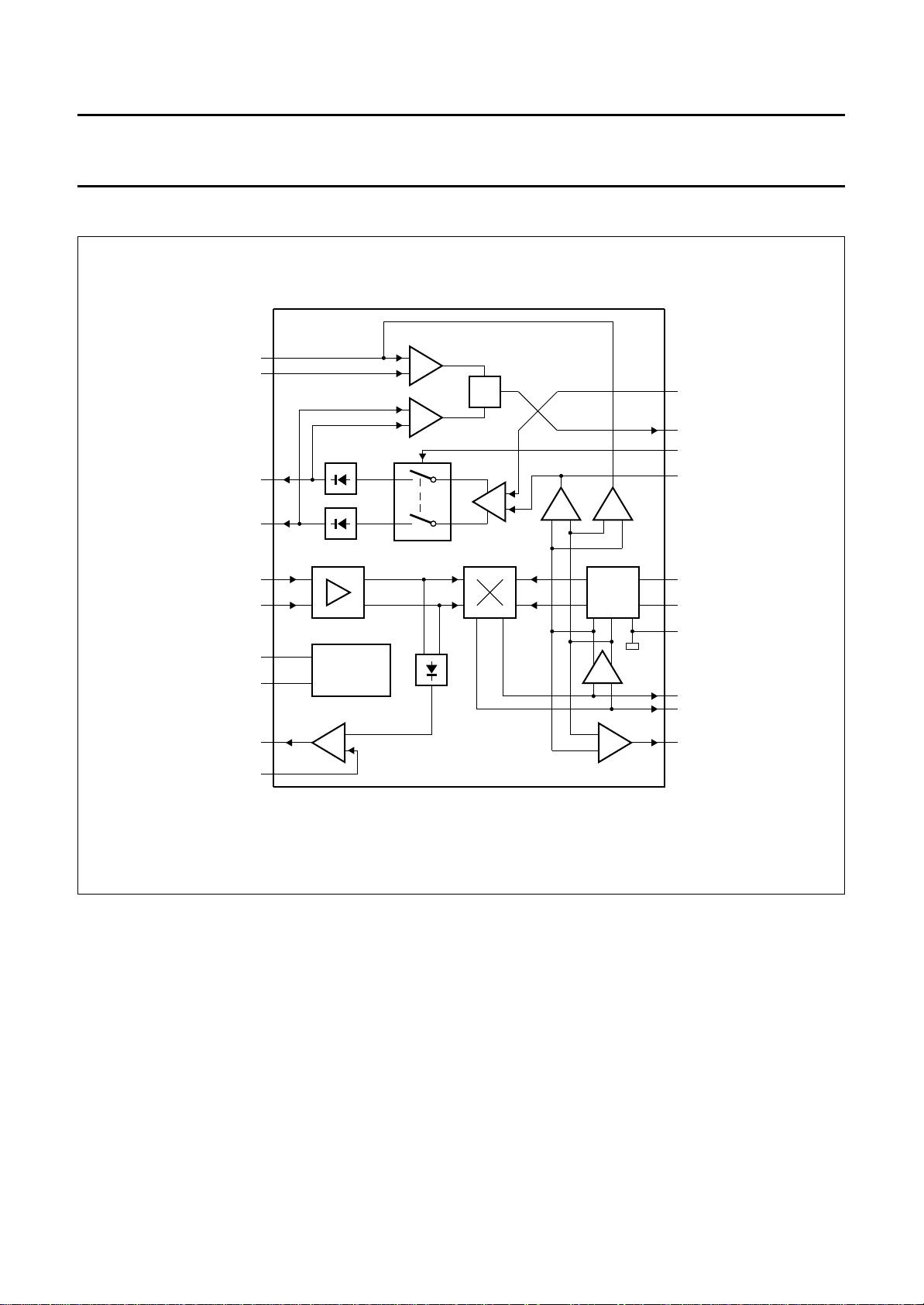
BLOCK DIAGRAM
handbook, full pagewidth
IFI1
IFI2
GND
V
CC
1
2
3
4
5
6
7
STABILIZER
8
AGC
9
10
th
CDF1
CDF2
PD(pos)
PD(neg)
AGCO
AGC
CARRIER
DETECTOR
AFC
TDA8012M
VCO
VIDEO BUFFER
20
19
18
17
16
15
14
13
12
11
TDA8012M
AFC
os
AFC
CDO
KEY
NF
VCO2
VCO1
OSCGND
LF2
LF1
VIDEO
MBE251
1996 Mar 26 3
Fig.1 Block diagram.
Philips Semiconductors Product specification
Low power PLL FM demodulator
for satellite TV receivers
PINNING
SYMBOL PIN DESCRIPTION
CDF1 1 carrier detector filter 1 input
CDF2 2 carrier detector filter 2 input
PD(pos) 3 positive peak detector output
PD(neg) 4 negative peak detector output
IFI1 5 IF input 1
IFI2 6 IF input 2
GND 7 ground
V
CC
AGCO 9 AGC output
AGC
th
VIDEO 11 baseband signal output
LF1 12 loop filter 1 input
LF2 13 loop filter 2 input
OSCGND 14 oscillator ground
VCO1 15 oscillator tank circuit 1 input
VCO2 16 oscillator tank circuit 2 input
NF 17 noise filter input
KEY 18 key pulse input
AFC
CDO
AFC
os
8 supply voltage
10 AGC threshold voltage input
19 AFC and carrier detector output
20 AFC offset input
dbook, halfpage
CDF1
1
2
CDF2
PD(pos)
PD(neg)
IFI1
3
4
5
TDA8012M
6
IFI2
7
GND
V
8
CC
AGCO
AGC
9
10
th
Fig.2 Pin configuration.
MBE250
TDA8012M
AFC
20
19
18
17
16
15
14
13
12
11
os
AFC
CDO
KEY
NF
VCO2
VCO1
OSCGND
LF2
LF1
VIDEO
FUNCTIONAL DESCRIPTION
The TDA8012M is a low power PLL FM demodulator
designed for use in satellite TV reception systems.
The demodulator is based on a Phase-Locked Loop (PLL)
structure including a fully balanced two-pin VCO. A high
gain IF amplifier ensures a high input sensitivity. The video
output voltage is supplied via a highly linear video buffer
which has a low output impedance. The centre frequency
of the VCO and the loop characteristics can be set using
external components.
The circuit provides an AGC signal which is used to drive
a gain-controlled IF amplifier (TDA8011T or TDA8010M)
to ensure a stable PLL demodulation characteristic.
An analog AFC voltage is also made available. This signal
can be suitably applied to the input of the ADC port of the
PLL frequency synthesizer (TSA5055). The AFC function
may be keyed to address D2MAC and MUSE systems.
The TDA8012M includes a Carrier Detector (CD) which is
used for channel detection during search procedures.
1996 Mar 26 4

Philips Semiconductors Product specification
Low power PLL FM demodulator
TDA8012M
for satellite TV receivers
LIMITING VALUES
In accordance with the Absolute Maximum Rating System (IEC 134).
SYMBOL PARAMETER MIN. MAX. UNIT
V
CC
V
i(max)
I
source(max)
t
sc
Z
L
T
stg
T
j
T
amb
HANDLING
Inputs and outputs are protected against electrostatic discharge in normal handling. However, to be totally safe it is
desirable to take normal precautions appropriate to handling MOS devices.
supply voltage −0.3 6.0 V
maximum input voltage on all pins −0.3 V
CC
V
maximum output source current − 10 mA
maximum short-circuit time on all outputs − 10 s
AC load impedance at video output 600 −Ω
storage temperature −55 +150 °C
junction temperature − +150 °C
operating ambient temperature −10 +80 °C
THERMAL CHARACTERISTICS
SYMBOL PARAMETER VALUE UNIT
R
th j-a
thermal resistance from junction to ambient in free air 120 K/W
CHARACTERISTICS
=5V; fi= 480 MHz; Vi=57dBµV; T
V
CC
=25°C; measured in application circuit of Fig.4;
amb
unless otherwise specified.
SYMBOL PARAMETER CONDITIONS MIN. TYP. MAX. UNIT
Supplies
V
CC
I
CC
supply voltage 4.75 5.0 5.25 V
supply current note 1 50 60 70 mA
Voltage controlled oscillator
K
VCO
δf
/δT voltage controlled oscillator drift note 2 −−70 × 10−6−°C
o
∆f
o
voltage controlled oscillator constant VCC= 4.75 to 5.25 V;
T
= −10 το +80 °C
amb
22.5 25 27.5 MHz/V
voltage controlled oscillator shift VCC= 4.75 to 5.25 V −− ±750 kHz
Frequency demodulator
V
i
Z
i
input signal voltage level note 3 53 57 61 dBµV
input impedance real part; note 4 − 50 −Ω
parallel inductive part;
− 130 − nH
note 4
K
PD
G
v
phase detector constant Vi=57dBµV − 0.37 − V/rad
phase-lock loop gain drift; note 5 − 2 − dB
shift; note 5 − 2 − dB
−1
1996 Mar 26 5

Philips Semiconductors Product specification
Low power PLL FM demodulator
TDA8012M
for satellite TV receivers
SYMBOL PARAMETER CONDITIONS MIN. TYP. MAX. UNIT
Z
o(diff)
CR
PLL
G
diff
Φ
diff
IM3 third-order intermodulation distortion note 8 50 −−dB
Video output
V
o(p-p)
V
O(DC)
Z
o
Automatic gain control (note 9)
AGC
th
LD level detector shift;
V
sat(AGC)
differential output impedance of the
1.6 2 2.4 kΩ
phase detector
phase-lock loop capture range note 6 −±17 − MHz
differential gain note 7 −±2 −%
differential phase note 7 −±2 −deg
baseband output signal amplitude
∆fo= 25 MHz 0.9 1.0 1.1 V
(peak-to-peak value)
DC voltage level of video output 2.1 2.35 2.6 V
output impedance − 10 50 Ω
AGC threshold as a function of the
voltage applied to pin 10
I
= 0.5 mA; 0.1V
AGC
= 0.5 mA; 0.9V
I
AGC
−− 53 dBµV
CC
61 −−dBµV
CC
− 1 − dB
= 4.75 to 5.25 V
V
CC
− 1 − dB
AGC steepness I
low level AGC output saturation
drift;
= −10 to +80 °C
T
amb
= 0.5 mA; note 10 − 8 − mA/dB
AGC
I
=1mA − 200 500 mV
AGC
voltage
Keying pulse
t
key
t
W(key)
V
IL
V
IH
Z
i
input keyed pulse time period − 64 −µs
keyed pulse width 8 −−µs
LOW level input keyed pulse voltage key on −− 0.8 V
HIGH level input keyed pulse voltage key off 2.7 −−V
input impedance 1 −−kΩ
AFC and carrier detector output (note 11)
δV
AFC
AFC/δf
shift
AFC steepness 4.9 5.5 6.1 V/MHz
shift of AFC voltage in relation to
VCO shift with unmodulated
480 MHz input signal
AFC
drift
drift of AFC voltage in relation to the
VCO
∆VCC= ±5% −±180 ±500 kHz
T
=80°C; note 12 −−400 − kHz
amb
1996 Mar 26 6

Philips Semiconductors Product specification
Low power PLL FM demodulator
TDA8012M
for satellite TV receivers
Notes
1. The DC supply current is defined for VCC=5V.
2. This typical value of −70 ppm/°C or −70 × 10−6°C−1 can be found in the reference measuring set-up shown in Fig.3.
The temperature drift may be adjusted by the temperature coefficient of the external capacitor in the tank circuit.
3. The circuit is designed for an input level of 57 dBµV. The maximum allowable input level is 61 dBµV. However, for
levels other than 57 dBµV the optimum loop filter values will be different from those given for the 57 dBµV input level
in the reference measuring set-up.
4. The input impedance is reduced to a resistor with a parallel reactance. The values are given at 480 MHz. In order to
reduce the radiation from the oscillator to the RF input, it is recommended to use a symmetrical drive.
5. The PLL loop gain shift and drift are given without loop filter shift and drift (non-temperature compensated external
components).
6. The capture range or lock-in range is defined as the PLL normal operating range. This value depends strongly on
the loop filter characteristics.
7. Measurements with test signals in accordance with CCIR recommendation 473-3. FM modulated signal with
DBS parameters:
a) 625 lines PAL TV system
b) 25 MHz/V modulator sensitivity
c) 1 V (p-p) video signal
d) No SAW filter is used.
8. No SAW filter is used at the input:
a) 16 MHz/V modulator sensitivity
b) 4.43 MHz sine wave colour signal [660 mV (p-p)]
c) 3.25 MHz sine wave luminance signal [700 mV (p-p)]
d) Two Wegner sound sub-carriers at 7.02 and 7.2 MHz (100 mV)
e) Intermodulation distance is defined as the distance between the luminance signal and the intermodulation
products.
9. The characteristics of the AGC function are measured in the application circuit of Fig.4. The circuit illustrated in Fig.4
has been designed to set the maximum AGC current of 1 mA. The output of the AGC function is capable of handling
up to 5 mA. The maximum AGC current can be increased to 5 mA by decreasing the value of the resistor connected
between pins 8 and 9.
10. In the application circuit (see Fig.4) the voltage at the AGC output decreases when the IF input level increases above
the adjusted AGC threshold.
11. The outputs from the AFC and carrier detector are combined at pin 19 (see Fig.3). During search tuning, when the
input frequency is outside the capture range, the combined output (carrier detector function) is at a LOW level
(any voltage below 0.6VCC). When the PLL becomes locked, the voltage at pin 19 rises to a HIGH level
(V19= 0.8VCCto VCC). When the input channel is close to the centre frequency, V19 falls to the LOW level. As shown
in Fig.3, the voltage at pin 19 is now a function of the centre frequency (AFC function). This information may be read
by a microcontroller via the ADC of the satellite frequency synthesizer (TSA5055) and the I2C-bus.
12. The drift of the AFC voltage is measured in accordance with the following method:
a) At room temperature (T
pin 20 must be adjusted to obtain a 1.5 V output at the AFC output (pin 19).
b) At T
therefore, be adjusted to obtain 1.5 V at the AFC output. The drift of the AFC voltage will then be equal to the
difference between the new input frequency and 480 MHz.
=80°C, due to its temperature drift, the AFC output voltage differs from 1.5V. The input frequency must,
amb
=25°C) the TDA8012M is driven by a 480 MHz unmodulated signal. The voltage at
amb
1996 Mar 26 7

Philips Semiconductors Product specification
Low power PLL FM demodulator
for satellite TV receivers
V19/V
CC
1
0.8
0.6
0.45
0.3
0.15
0
carrier detect on
500 kHz
TDA8012M
MBE253
AFC DATA
f
o
frequency
Fig.3 AFC and carrier detector output.
1996 Mar 26 8

Philips Semiconductors Product specification
Low power PLL FM demodulator
for satellite TV receivers
APPLICATION INFORMATION
book, full pagewidth
IF input
V
CC
AGCO
1 µF
82 kΩ
2.7 MΩ
22 µF
330 nF
10 MΩ
330 nF
10 MΩ
47
kΩ
10 nF
10 nF
4.7
kΩ
1
2
3
4
5
6
7
8
9
10
STABILIZER
AGC
CARRIER
DETECTOR
AFC
TDA8012M
VCO
VIDEO BUFFER
MBE252
TDA8012M
V
CC
36 kΩ
2.2 kΩ
20
13 kΩ
19
18
17
16
15
14
13
12
11
10
kΩ
180 pF
2
kΩ
VIDEO
KEY
10 pF
1.3
kΩ
1 µF
1.2 pF30 nH
AFC
CDO
1996 Mar 26 9
Fig.4 Application circuit.

Philips Semiconductors Product specification
Low power PLL FM demodulator
for satellite TV receivers
PACKAGE OUTLINE
SSOP20: plastic shrink small outline package; 20 leads; body width 4.4 mm
D
c
20
y
Z
11
H
TDA8012M
SOT266-1
E
E
A
X
v M
A
pin 1 index
110
w M
b
e
DIMENSIONS (mm are the original dimensions)
mm
A
max.
1.5
0.1501.4
1.2
0.25
b
3
p
0.32
0.20
UNIT A1A2A
Note
1. Plastic or metal protrusions of 0.20 mm maximum per side are not included.
p
cD
0.20
6.6
0.13
6.4
0 2.5 5 mm
scale
(1)E(1)
eHELLpQZywv θ
4.5
0.65 1.0 0.2
4.3
6.6
6.2
Q
A
2
A
1
detail X
0.65
0.75
0.45
0.45
(A )
L
p
L
A
3
θ
0.13 0.1
0.48
0.18
(1)
o
10
o
0
OUTLINE
VERSION
SOT266-1
1996 Mar 26 10
REFERENCES
IEC JEDEC EIAJ
EUROPEAN
PROJECTION
ISSUE DATE
90-04-05
95-02-25

Philips Semiconductors Product specification
Low power PLL FM demodulator
for satellite TV receivers
SOLDERING
Introduction
There is no soldering method that is ideal for all IC
packages. Wave soldering is often preferred when
through-hole and surface mounted components are mixed
on one printed-circuit board. However, wave soldering is
not always suitable for surface mounted ICs, or for
printed-circuits with high population densities. In these
situations reflow soldering is often used.
This text gives a very brief insight to a complex technology.
A more in-depth account of soldering ICs can be found in
“IC Package Databook”
our
Reflow soldering
Reflow soldering techniques are suitable for all SSOP
packages.
Reflow soldering requires solder paste (a suspension of
fine solder particles, flux and binding agent) to be applied
to the printed-circuit board by screen printing, stencilling or
pressure-syringe dispensing before package placement.
Several techniques exist for reflowing; for example,
thermal conduction by heated belt. Dwell times vary
between 50 and 300 seconds depending on heating
method. Typical reflow temperatures range from
215 to 250 °C.
Preheating is necessary to dry the paste and evaporate
the binding agent. Preheating duration: 45 minutes at
45 °C.
Wave soldering
Wave soldering isnot recommended for SSOP packages.
This is because of the likelihood of solder bridging due to
closely-spaced leads and the possibility of incomplete
solder penetration in multi-lead devices.
(order code 9398 652 90011).
TDA8012M
If wave soldering cannot be avoided, the following
conditions must be observed:
• A double-wave (a turbulent wave with high upward
pressure followed by a smooth laminar wave)
soldering technique should be used.
• The longitudinal axis of the package footprint must
be parallel to the solder flow and must incorporate
solder thieves at the downstream end.
Even with these conditions, only consider wave
soldering SSOP packages that have a body width of
4.4 mm, that is SSOP16 (SOT369-1) or
SSOP20 (SOT266-1).
During placement and before soldering, the package must
be fixed with a droplet of adhesive. The adhesive can be
applied by screen printing, pin transfer or syringe
dispensing. The package can be soldered after the
adhesive is cured.
Maximum permissible solder temperature is 260 °C, and
maximum duration of package immersion in solder is
10 seconds, if cooled to less than 150 °C within
6 seconds. Typical dwell time is 4 seconds at 250 °C.
A mildly-activated flux will eliminate the need for removal
of corrosive residues in most applications.
Repairing soldered joints
Fix the component by first soldering two diagonallyopposite end leads. Use only a low voltage soldering iron
(less than 24 V) applied to the flat part of the lead. Contact
time must be limited to 10 seconds at up to 300 °C. When
using a dedicated tool, all other leads can be soldered in
one operation within 2 to 5 seconds between
270 and 320 °C.
1996 Mar 26 11

Philips Semiconductors Product specification
Low power PLL FM demodulator
TDA8012M
for satellite TV receivers
DEFINITIONS
Data sheet status
Objective specification This data sheet contains target or goal specifications for product development.
Preliminary specification This data sheet contains preliminary data; supplementary data may be published later.
Product specification This data sheet contains final product specifications.
Limiting values
Limiting values given are in accordance with the Absolute Maximum Rating System (IEC 134). Stress above one or
more of the limiting values may cause permanent damage to the device. These are stress ratings only and operation
of the device at these or at any other conditions above those given in the Characteristics sections of the specification
is not implied. Exposure to limiting values for extended periods may affect device reliability.
Application information
Where application information is given, it is advisory and does not form part of the specification.
LIFE SUPPORT APPLICATIONS
These products are not designed for use in life support appliances, devices, or systems where malfunction of these
products can reasonably be expected to result in personal injury. Philips customers using or selling these products for
use in such applications do so at their own risk and agree to fully indemnify Philips for any damages resulting from such
improper use or sale.
1996 Mar 26 12
 Loading...