


INTEGRATED CIRCUITS
DATA SH EET
TDA5736; TDA5737
5 V VHF, hyperband and UHF
mixer/oscillators for TV and VCR
3-band tuners
Product specification
Supersedes data of 1996 Oct 16
File under Integrated Circuits, IC02
1996 Oct 25

Philips Semiconductors Product specification
5 V VHF, hyperband and UHF mixer/oscillators
for TV and VCR 3-band tuners
FEATURES
• Balanced mixer with a common emitter input for band A
(single input)
• 2-pin oscillator for band A
• Balanced mixer with a common base input for bands B
and C (balanced input)
• 3-pin oscillator for band B
• 4-pin oscillator for band C
• Local oscillator buffer output for external prescaler
• SAW filter preamplifier with a low output impedance to
drive the SAW filter directly
• Band gap voltage stabilizer for oscillator stability
• Electronic band switch
• External IF filter between the mixer output and the IF
amplifier input.
APPLICATIONS
GENERAL DESCRIPTION
The TDA5736 and TDA5737 are monolithic integrated
circuits that perform the mixer/oscillator functions for
bands A, B and C in TV and VCR tuners. These low power
mixer/oscillators require a power supply of 5 V and are
available in a very small package.
These devices give the designer the capability to design
an economical and physically small 3-band tuner.
They are suitable for European standards, as illustrated in
Fig.17, with the following RF bands: 48.25 to 168.25 MHz,
175.25 to 447.25 MHz and 455.25 to 855.25 MHz.
With an appropriate tuned circuit, they are also suitable for
NTSC all channel tuners (USA and Japan).
The tuner development time can be drastically reduced by
using these devices.
TDA5736; TDA5737
• 3-band all channel TV and VCR tuners
• Any standard.
QUICK REFERENCE DATA
SYMBOL PARAMETER CONDITIONS MIN. TYP. MAX. UNIT
V
P
I
P
f
RF
G
v
NF noise figure band A − 7.5 − dB
V
o
Note
1. The limits are related to the tank circuits used in Fig.17 and the intermediate frequency. Frequency bands may be
adjusted by the choice of external components.
supply voltage − 5.0 − V
supply current − 50 − mA
frequency range RF input; band A; note 1 41 − 171 MHz
RF input; band B; note 1 166 − 451 MHz
RF input; band C; note 1 446 − 861 MHz
voltage gain band A − 23 − dB
band B − 34 − dB
band C − 34 − dB
band B − 8 − dB
band C − 9 − dB
output voltage level causing
1% cross modulation in
channel
band A − 116 − dBµV
band B − 115 − dBµV
band C − 115 − dBµV
1996 Oct 25 2
Philips Semiconductors Product specification
5 V VHF, hyperband and UHF mixer/oscillators for
TDA5736; TDA5737
TV and VCR 3-band tuners
ORDERING INFORMATION
TYPE
NUMBER
NAME DESCRIPTION VERSION
TDA5736M SSOP24 plastic shrink small outline package; 24 leads; body width 5.3 mm SOT340-1
TDA5737M SSOP24 plastic shrink small outline package; 24 leads; body width 5.3 mm SOT340-1
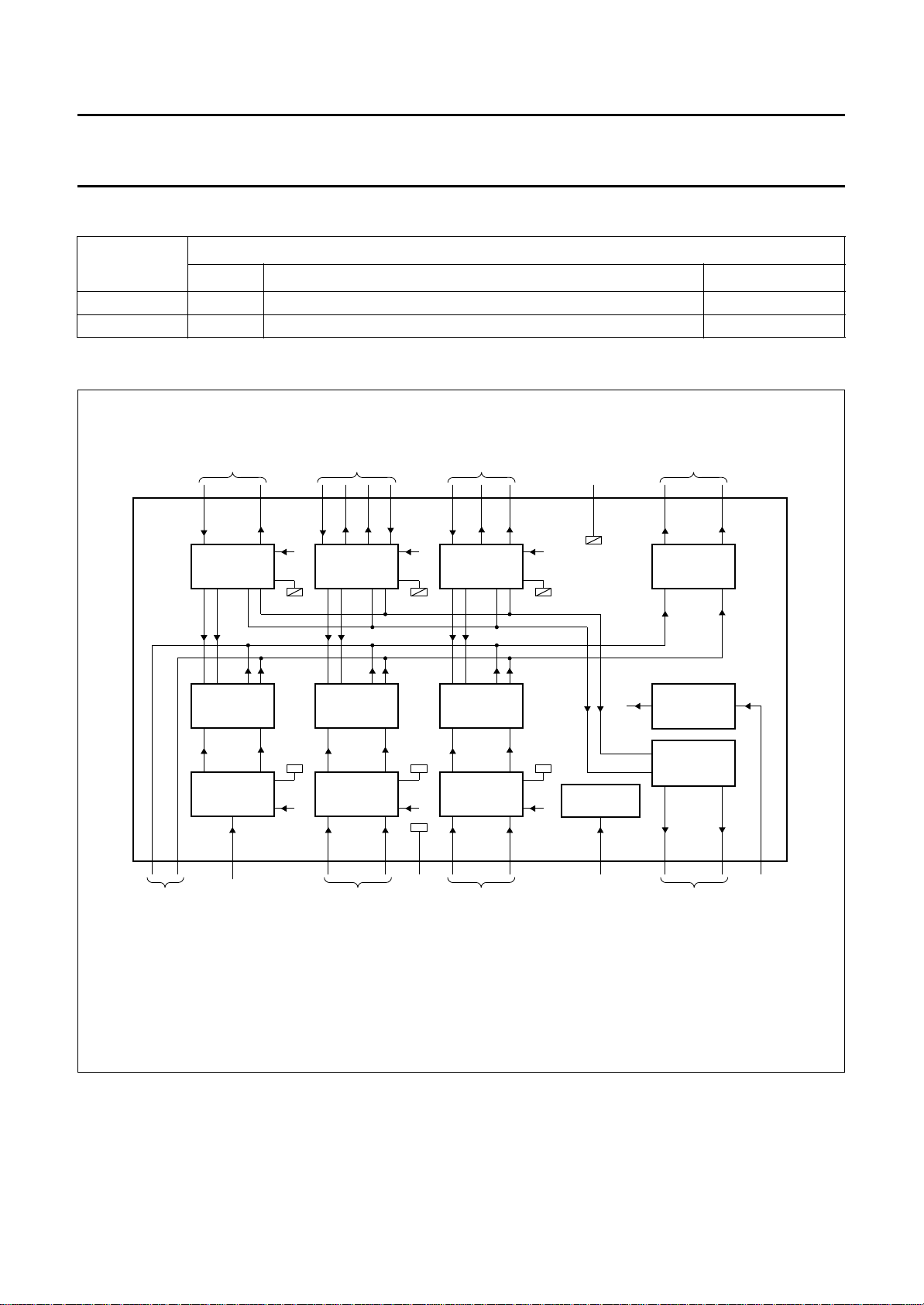
BLOCK DIAGRAM
handbook, full pagewidth
band A oscillator
tuned cicuit
23
(2)
BAND A
OSCILLATOR
21
(4)
band C oscillator
tuned cicuit
22
24
20
(3)
(1)
(5)
BAND C
OSCILLATOR
18
(7)
PACKAGE
band B oscillator
tuned cicuit
19
17
(6)
(8)
BAND B
OSCILLATOR
16
(9)
GND
15
(10)
TDA5736M
TDA5737M
IF outputs
14
(11)
IF
AMPLIFIER
13
(12)
MIXER MIXER MIXER
BAND A
STAGE
(24)1(23)
2
IF
filter input
The numbers in parenthesis represent the TDA5737M.
(19)
6
band A
input
BAND C
STAGE
(21)
4
band C
inputs
BAND B
STAGE
(20)5(22)3(18)
GND
RF
7
band B
inputs
Fig.1 Block diagram.
(17)
8
DC
STABILIZER
(16)
9
V
P
ELECTRONIC
BAND
SWITCH
LOCAL
OSCILLATOR
AMPLIFIER
(15)
10
local oscillator
amplifier outputs
(14)11(13)
12
band switch
input
MGE971
1996 Oct 25 3

Philips Semiconductors Product specification
5 V VHF, hyperband and UHF mixer/oscillators for
TV and VCR 3-band tuners
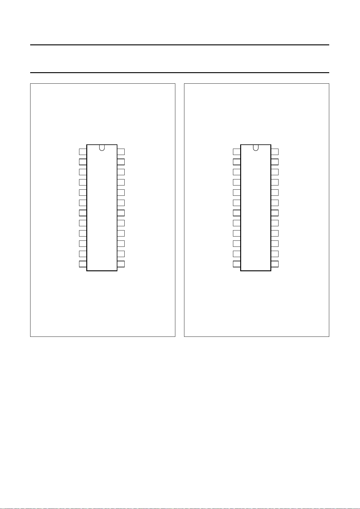
PINNING
SYMBOL
IFIN1 1 24 IF filter input 1
IFIN2 2 23 IF filter input 2
RFGND 3 22 ground for RF inputs
CIN1 4 21 band C input 1
CIN2 5 20 band C input 2
AIN 6 19 band A input
BIN1 7 18 band B input 1
BIN2 8 17 band B input 2
V
P
LOOUT1 10 15 local oscillator amplifier output 1
LOOUT2 11 14 local oscillator amplifier output 2
BS 12 13 band switch input
IFOUT1 13 12 IF amplifier output 1
IFOUT2 14 11 IF amplifier output 2
GND 15 10 ground (0 V)
BOSCOC1 16 9 band B oscillator output collector 1
BOSCOC2 17 8 band B oscillator output collector 2
COSCIB1 18 7 band C oscillator input base 1
BOSCIB 19 6 band B oscillator input base
COSCOC1 20 5 band C oscillator output collector 1
AOSCOC 21 4 band A oscillator output collector
COSCOC2 22 3 band C oscillator output collector 2
AOSCIB 23 2 band A oscillator input base
COSCIB2 24 1 band C oscillator input base 2
TDA5736 TDA5737
PIN
DESCRIPTION
9 16 supply voltage
TDA5736; TDA5737
1996 Oct 25 4
Philips Semiconductors Product specification
5 V VHF, hyperband and UHF mixer/oscillators for
TV and VCR 3-band tuners
handbook, halfpage
1
IFIN1 COSCIB2
2
IFIN2
RFGND
LOOUT1
LOOUT2
CIN1
CIN2
AIN
BIN1
BIN2
V
BS
P
3
4
5
6
TDA5736M
7
8
9
10
11
12
MBE383
24
23
AOSCIB
22
COSCOC2
AOSCOC
21
20
COSCOC1
19
BOSCIB
COSCIB1
18
BOSCOC2
17
16
BOSCOC1
15
GND
IFOUT2
14
13
IFOUT1
handbook, halfpage
AOSCIB
COSCOC2
AOSCOC
COSCOC1
BOSCIB
COSCIB1
BOSCOC2
BOSCOC1
GND
IFOUT2
IFOUT1
TDA5736; TDA5737
1
2
3
4
5
6
TDA5737M
7
8
9
10
11
12
MGE970
24
23
22
21
20
19
18
17
16
15
14
13
IFIN1COSCIB2
IFIN2
RFGND
CIN1
CIN2
AIN
BIN1
BIN2
V
P
LOOUT1
LOOUT2
BS
Fig.2 Pin configuration (TDA5736M).
1996 Oct 25 5
Fig.3 Pin configuration (TDA5737M).
Philips Semiconductors Product specification
5 V VHF, hyperband and UHF mixer/oscillators for
TDA5736; TDA5737
TV and VCR 3-band tuners
LIMITING VALUES
In accordance with the Absolute Maximum Rating System (IEC 134).
SYMBOL PARAMETER MIN. MAX. UNIT
V
P
V
SW
V
n(max)
I
O
t
sc(max)
T
stg
T
amb
T
j
HANDLING
Human Body Model:
• For TDA5736 GND (15), RFGND (3), V
• For TDA5737 GND (10), RFGND (22), VP(16) separate.
supply voltage −0.3 +7.0 V
switching voltage −0.3 +7.0 V
maximum voltage on each pin with a 22 kΩ resistor
− 35 V
connected in series
output current of each pin to ground −−10 mA
maximum short-circuit time (all pins) − 10 s
IC storage temperature −55 +150 °C
operating ambient temperature −20 +80 °C
junction temperature − +150 °C
(9) separate
P
All pins withstand 2000 V in accordance with the
“MIL-STD-883C”
category B (2000 V) except pins 16 and 17 (8 and 9 for the TDA5737) which withstand 1000 V;
“UZW-BO/FQ-A302”
. Philips specification equivalent to the
R = 1500 Ω, C = 100 pF.
Machine Model:
• For TDA5736 GND (15), RFGND (3), VP(9) separate
• For TDA5737 GND (10), RFGND (22), VP(16) separate.
All pins withstand 200 V in accordance with the
“UZW-BO/FQ-B302”
, Philips specification (revision of: Nov. 6th, 1990)
except pins 16 and 17 (8 and 9 for the TDA5737) which withstand 100 V; R = 0 Ω, C = 200 pF.
THERMAL CHARACTERISTICS
SYMBOL PARAMETER CONDITIONS VALUE UNIT
R
th j-a
thermal resistance from junction to ambient in free air 120 K/W
1996 Oct 25 6
Philips Semiconductors Product specification
5 V VHF, hyperband and UHF mixer/oscillators for
TDA5736; TDA5737
TV and VCR 3-band tuners
CHARACTERISTICS
V
=5V; T
P
SYMBOL PARAMETER CONDITIONS MIN. TYP. MAX. UNIT
Supply
V
P
I
P
V
SW
I
SW
Band A mixer (including IF amplifier)
f
RF
G
v
NF noise figure f
V
o
V
i
g
os
Y
i
C
i
Band A oscillator
f
osc
f
shift
f
drift
V
ripple
Φ
N
=25°C; measured in circuit of Fig.17; unless otherwise specified.
amb
supply voltage 4.5 5.0 5.5 V
supply current 42 50 58 mA
switching voltage depending
on supply voltage V
P
band A; note 1 0 − 0.18VPV
band B; note 1 0.26V
band C; note 1 0.55V
− 0.47VPV
P
− V
P
P
V
switching current band A; note 1 −−2µA
band B; note 1 −−10 µA
band C; note 1 −−25 µA
frequency range note 2 41 − 171 MHz
voltage gain fRF= 50 MHz; see Fig.4; note 3 20.5 23.0 25.5 dB
= 170 MHz; see Fig.4; note 3 20.5 23.0 25.5 dB
f
RF
= 50 MHz; see Figs.5 and 6 − 7.5 9 dB
RF
= 170 MHz; see Figs.5 and 6 − 910dB
f
RF
output voltage level causing
1% cross modulation in
channel
input voltage level causing
fRF= 50 MHz; see Fig.7 115 118 − dBµV
= 170 MHz; see Fig.7 113 116 − dBµV
f
RF
fRF= 170 MHz; note 4 96 100 − dBmV
10 kHz pulling in channel
optimum source conductance
for noise figure
fRF=50MHz − 0.5 − mS
= 170 MHz − 1.1 − mS
f
RF
input admittance fRF= 50 to 170 MHz; see Fig.12 − 0.3 − mS
input capacitance fRF= 50 to 170 MHz; see Fig.12 − 1.9 − pF
frequency range 0.45 V < Vt< 28 V; notes 1 and 5 80 − 210 MHz
frequency shift ∆Vp= 5%; note 6 −−53 kHz
frequency drift with no
compensation
∆T=25°C; NP0 capacitors; note7 −−650 kHz
5 s to 15 mins after switch on; NP0
−−250 kHz
capacitors; note 8
frequency drift with
compensation
∆T=25°C; notes7 and 9;
see Fig.18
5 s to 15 mins after switch on;
−−500 kHz
−−100 kHz
notes 8 and 9; see Fig.18
ripple susceptibility of supply
voltage (peak-to-peak value)
f
= 80 MHz;
osc
4.75 V < VP< 5.25 V; see Fig.8
f
= 210 MHz;
osc
20 −− mV
20 −− mV
4.75 V < VP< 5.25 V; see Fig.8
phase noise measured at the IF output at 10 kHz
81 −− dBc/Hz
offset; Vo= 105 dBµV
1996 Oct 25 7
Philips Semiconductors Product specification
5 V VHF, hyperband and UHF mixer/oscillators for
TDA5736; TDA5737
TV and VCR 3-band tuners
SYMBOL PARAMETER CONDITIONS MIN. TYP. MAX. UNIT
Band B mixer (including IF amplifier)
f
RF
G
v
N noise figure
V
o
V
i
Z
i
Band B oscillator
f
osc
f
shift
f
drift
V
ripple
Φ
N
frequency range note 2 166 − 451 MHz
voltage gain fRF= 170 MHz; see Fig.9; note 3 31 34 37 dB
= 450 MHz; see Fig.9; note 3 31 34 37 dB
f
RF
= 170 MHz; see Fig.10 − 810dB
f
RF
(not corrected for image)
output voltage level causing
1% cross modulation in
channel
input voltage level causing
f
= 450 MHz; see Fig.10 − 810dB
RF
fRF= 170 MHz; see Fig.7 114 117 − dBµV
= 450 MHz; see Fig.7 112 115 − dBµV
f
RF
fRF= 450 MHz; note 4 83 87 − dBµV
10 kHz pulling in channel
input impedance (Rs+jLsω)fRF= 170 to 450 MHz; see Fig.13 − 23 −Ω
f
= 170 to 450 MHz; see Fig.13 − 9 − nH
RF
frequency range 0.45 V < Vt< 28 V; notes 1 and 5 205 − 490 MHz
frequency shift ∆Vp= 5%; note 6 −−53 kHz
frequency drift with no
compensation
∆T=25°C; NP0 capacitors; note7 −−2000 kHz
5 s to 15 mins after switch on; NP0
−−750 kHz
capacitors; note 8
frequency drift with
compensation
∆T=25°C; notes7 and 9;
see Fig.18
5 s to 15 mins after switch on;
−−750 kHz
−−300 kHz
notes 8 and 9; see Fig.18
ripple susceptibility of supply
voltage (peak-to-peak value)
f
= 250 MHz;
osc
4.75 V < VP< 5.25 V; see Fig.8
f
= 490 MHz;
osc
20 −− mV
20 −− mV
4.75 V < VP< 5.25 V; see Fig.8
phase noise measured at the IF output at 10 kHz
81 −− dBc/Hz
offset; Vo= 105 dBmV
Band C Mixer (including IF amplifier)
f
RF
G
v
frequency range note 2 446 − 861 MHz
voltage gain fRF= 450 MHz; see Fig.9; note 3 31 34 37 dB
N noise figure
(not corrected for image)
V
o
output voltage level causing
1% cross modulation in
channel
V
i
input voltage level causing
10 kHz pulling in channel
Z
I
input impedance (Rs+jLsω)fRF= 450 to 860 MHz; see Fig.14 − 28 −Ω
1996 Oct 25 8
= 860 MHz; see Fig.9; note 3 31 34 37 dB
f
RF
= 450 MHz; see Fig.10 − 911dB
f
RF
= 860 MHz; see Fig.10 − 911dB
f
RF
fRF= 450 MHz; see Fig.7 112 115 − dBµV
= 860 MHz; see Fig.7 112 115 − dBµV
f
RF
fRF= 860 MHz; note 4 91 95 − dBµV
= 450 to 860 MHz; see Fig.14 − 10 − nH
f
RF

Philips Semiconductors Product specification
5 V VHF, hyperband and UHF mixer/oscillators for
TDA5736; TDA5737
TV and VCR 3-band tuners
SYMBOL PARAMETER CONDITIONS MIN. TYP. MAX. UNIT
Band C oscillator
f
f
f
V
Φ
osc
shift
drift
ripple
N
frequency range 0.45 V < Vt< 28 V; notes 1 and 5 485 − 900 MHz
frequency shift ∆VP= 5%; note 6 −−53 kHz
frequency drift with no
compensation
∆T=25°C; NP0 capacitors; note7 −−2800 kHz
5 s to 15 mins after switch on; NP0
−−700 kHz
capacitors; note 8
frequency drift with
compensation
∆T=25°C; notes7 and 9;
see Fig.18
5 s to 15 mins after switch on;
−−1000 kHz
−−250 kHz
notes 8 and 9; see Fig.18
ripple susceptibility of supply
voltage (peak to peak value)
f
= 485 MHz;
osc
4.75 V < VP< 5.25 V; see Fig.8
= 900 MHz;
f
osc
20 −− mV
18 −− mV
4.75 V < VP< 5.25 V; see Fig.8
phase noise measured at the IF output at 10 kHz
81 −− dBc/Hz
offset; Vo= 105 dBµV
LO output
Z
O
V
o
SRF spurious signal on LO output
output admittance (YP+jωCP)YP= 80 MHz; see Fig.12 − 2.5 − mS
= 900 MHz; see Fig.12 − 5 − mS
Y
P
; see Fig.12 − 0.9 − pF
C
P
output voltage RL=50Ω; 0<Vt< 35 V 80 91 100 dBµV
with respect to LO output
=50Ω; 0.2V<Vt<35V;
R
L
notes 1 and 10
−−−10 dB
signal
HLO LO signal harmonics with
=50Ω; 0<Vt< 35 V; note 1 −−−10 dB
R
L
respect to LO signal
IF amplifier
S
22
output reflection coefficient magnitude; see Fig.15 −−16 − dB
phase; see Fig.15 − 12 − deg.
Z
O
output impedance (Rs+jLsω)R
s
L
s
− 67 −Ω
− 20 − nH
Notes
1. −20 °C<T
< +80 °C; 4.5 V < VP< 5.5 V.
amb
2. The RF frequency range is defined by the oscillator frequency range and the intermediate frequency.
3. The gain is defined as the transducer gain (measured in Fig.17) plus the voltage transformation ratio of L7 to L8
(10 : 2, 15.4 dB including transformer loss).
4. The input level causing 10 kHz frequency detuning at the LO output. f
osc=fRF
+ 33.4 MHz.
5. Limits are related to the tank circuits used in Fig.17. Frequency bands may be adjusted by the choice of external
components.
6. The frequency shift is defined as the change in oscillator frequency when the supply voltage varies from
VP= 5 to 4.75 V and from VP= 5 to 5.25 V.
1996 Oct 25 9

Philips Semiconductors Product specification
5 V VHF, hyperband and UHF mixer/oscillators for
TDA5736; TDA5737
TV and VCR 3-band tuners
7. The frequency drift is defined as the change in oscillator frequency when the ambient temperature varies from
T
=25to0°C and from T
amb
8. Switch-on drift is defined as the change in oscillator frequency between 5 s and 15 mins after switch on.
9. With thermal compensation, the capacitors of the tank circuits have the following temperature coefficients:
a) In band A: C1, C6 and C8 are N750.
b) In band B: C4, C11, C12, C13 and C36 are N750.
c) In band C: C5, C7, C9 and C10 are N750; C2 is N220 and C3 is NP0.
10. SRF: spurious signal on LO with respect to LO output signal;
a) RF level = 120 dBµV at fRF< 180 MHz.
b) RF level = 107.5 dBµV at fRF= 180 to 225 MHz.
c) RF level = 97 dBµV at fRF= 225 to 860 MHz.
handbook, full pagewidth
e
50 Ω
V
meas
signal
source
=25to50°C.
amb
V
50 Ω
RMS
voltmeter
o
2 x 5
turns
TR
2
turns
N1/N2 = 5
V'
meas
spectrum
analyzer
50 Ω
MGD264
AIN
V
i
D.U.T.
GND
IF
out
V
IF
out
ZI (AIN) >> 50 Ω Vi=2×V
Vi=V
Vo=V
Gv= 20 log (Vo/Vi).
+ 6 dB.
meas
+ 15.4 dB (transformer ratio N1/N2 = 5 and transformer loss).
’meas
meas
.
Fig.4 Band A gain measurement.
1996 Oct 25 10
Philips Semiconductors Product specification
5 V VHF, hyperband and UHF mixer/oscillators for
TV and VCR 3-band tuners
handbook, full pagewidth
C1
BNC BNC
L1 C2
(a) For fRF= 50 MHz:
mixer A frequency response measured = 57 MHz, loss = 0 dB
image suppression = 16 dB.
C1 = 9 pF
C2=15pF
L1 = 7 turns (diam. = 5.5 mm, wire diam. = 0.5 mm)
I1 = semi rigid cable (RIM): 5 cm long (semi rigid cable (RIM);
33 dB/100 m; 50 Ω; 96 pF/m).
I1
RIM-RIM
PCB
C3
plug plug
(a) (b)
(b) For fRF= 150 MHz:
mixer A frequency response measured = 150.3 MHz, loss = 1.3 dB
image suppression = 13 dB.
C3 = 5 pF
C4=25pF
I2 = semi rigid cable (RIM): 30 cm long
I3 = semi rigid cable (RIM): 5 cm long (semi rigid cable (RIM);
33 dB/100 m; 50 Ω; 96 pF/m).
C4
TDA5736; TDA5737
I3
I2
RIM-RIM
PCB
MBE286 - 1
handbook, full pagewidth
NOISE
SOURCE
Fig.5 Input circuit for optimum noise figure in band A.
BNC RIM
INPUT
CIRCUIT
(see Fig. 5)
AIN
GND
IFOUT1
D.U.T.
IFOUT2
TR
2 x 5
turns
N1/N2 = 5
MBH046
NOISE
METER
2
turns
NF = NF
− loss (input circuit) dB.
meas
1996 Oct 25 11
Fig.6 Noise figure measurement in band A.

Philips Semiconductors Product specification
5 V VHF, hyperband and UHF mixer/oscillators for
TV and VCR 3-band tuners
handbook, full pagewidth
e
e
V’
meas=Vo
Wanted output signal at f
We measure the level of the unwanted signal Vou causing 1% AM modulation in the wanted output signal; f
= 83.9 MHz (203.9 MHz).
f
osc
Vou=V’
meas
Filter characteristics: fc= 33.9 MHz, f
unwanted
signal
source
50 Ω
AM = 30%
u
50 Ω
w
−15.4 dB (transformer ratio N1/N2 = 5 and transformer loss).
wanted
source
+ 15.4 dB.
AC
HYBRID
BD
signal
= 50 MHz (170 MHz); Vow=80dBµV.
RFW
−3dBBW
50
Ω
= 1 MHz; f
V
IMA
RFA
−30dBBW
D.U.T.
= 2.3 MHz.
out
out
IF
V
o
2 x 5
turns
IF
2
turns
N1/N2 = 5
TDA5736; TDA5737
18 dB
attenuator
V
RMS
voltmeter
RFU
V'
FILTER
33.9 MHz
meas
= 45.5 MHz (165.5 MHz);
modulation
analyzer
50 Ω
MGE972
Fig.7 Cross modulation measurement in band A.
handbook, full pagewidth
The ripple susceptibility is defined as the level of a signal added to the supply voltage causing sidebands in the LO output at 53.5 dBc.
This signal has a frequency between 20 Hz and 500 kHz.
DC supply
6.8 kΩ
100 µF 100 µF
ripple
signal
V
47 Ω
P
REFERENCE
MEASUREMENT
SET-UP
OF FIG. 17
WITHOUT
L10, C25, C35, C26
to
spectrum
analyser
53.5 dBc
−500 kHz +500 kHz
f
o
MGE974
1996 Oct 25 12
Fig.8 Ripple susceptibility.

Philips Semiconductors Product specification
5 V VHF, hyperband and UHF mixer/oscillators for
TV and VCR 3-band tuners
handbook, full pagewidth
e
loss
Vi=V
Vo=V’
Voltage gain for band B and C = 20 log (Vo/Vi).
= 1 dB.
(hybrid)
− loss
meas
+ 15.4 dB (transformer ratio N1/N2 and transformer loss).
meas
50 Ω
(hybrid)
V
.
meas
signal
source
V
RMS
voltmeter
50 Ω
50 Ω
AC
HYBRID
BD
CIN1
IFOUT1
V
i
D.U.T.
CIN2
IFOUT2
TDA5736; TDA5737
TR
V
o
2 x 5
turns
2
turns
N1/N2 = 5
V'
meas
spectrum
analyzer
50 Ω
MBH048
handbook, full pagewidth
Loss of the hybrid: 1 dB.
NF = NF
− loss of the hybrid.
meas
NOISE
SOURCE
Fig.9 Gain measurement in bands B and C.
AC
HYBRID
BD
50 Ω
CIN1
CIN2
IFOUT1
D.U.T.
IFOUT2
2 x 5
turns
N1/N2 = 5
TR
NOISE
METER
2
turns
MBH049
1996 Oct 25 13
Fig.10 Noise figure measurement in bands B and C.

Philips Semiconductors Product specification
5 V VHF, hyperband and UHF mixer/oscillators for
TV and VCR 3-band tuners
handbook, full pagewidth
e
e
V’
meas=Vo
Wanted output signal at f
We measure the level of the unwanted signal Vou causing 1% AM modulation in the wanted output signal;
f
RFU
Vou=V’
Filter characteristics: fc= 33.9 MHz, f
unwanted
signal
source
50 Ω
AM = 30%
u
50 Ω
w
wanted
source
−15.4 dB (transformer ratio N1/N2 = 5 and transformer loss).
= 165.5 or 445.5 MHz (445.5 or 855.5 MHz); f
+ 15.4 dB.
meas
signal
AC
HYBRID
BD
50
Ω
= 170 or 450 MHz (450 or 860 MHz); Vow=70dBµV.
RFW
−3dBBW
V
IMB
(V
IMC
50
Ω
= 1 MHz; f
AC
HYBRID
)
BD
OSC
RFB
(RFC)
D.U.T.
RFB
(RFC)
= 203.9 or 483.9 MHz (483.9 or 893.9 MHz).
= 2.3 MHz.
−30dBBW
out
out
IF
V
o
2 x 5
turns
IF
N1/N2 = 5
TDA5736; TDA5737
FILTER
33.9 MHz
2
turns
18 dB
attenuator
V
RMS
voltmeter
modulation
analyzer
50 Ω
MGE973
handbook, full pagewidth
Fig.11 Cross modulation measurement in bands B and C.
1
2
5
10
∞
10
5
2
1
0.5
0.20.512510
200 MHz
0.5
40 MHz
MBH055
0.2
0
0.2
– j
+ j
Fig.12 Input admittance (S11) of the band A mixer input (40 to 200 MHz); Yo= 20 mS.
1996 Oct 25 14

Philips Semiconductors Product specification
5 V VHF, hyperband and UHF mixer/oscillators for
TV and VCR 3-band tuners
handbook, full pagewidth
0.5
470 MHz
0.2
+ j
0
– j
0.2
170 MHz
0.5 10.2 1052
0.5
1
TDA5736; TDA5737
2
5
10
∞
10
5
2
handbook, full pagewidth
1
MBH053
Fig.13 Input impedance (S11) of the band B mixer input (170 to 470 MHz); Zo=50Ω.
1
0.5
860 MHz
0.2
460 MHz
+ j
0
– j
0.2
0.5 10.2 1052
2
5
10
∞
10
5
Fig.14 Input impedance (S11) of the band C mixer input (460 to 860 MHz); Zo=50Ω.
1996 Oct 25 15
0.5
2
1
MBH054

Philips Semiconductors Product specification
5 V VHF, hyperband and UHF mixer/oscillators for
TV and VCR 3-band tuners
handbook, full pagewidth
0.5
0.2
+ j
0
– j
0.2
0.5
0.5 10.2 1025
1
45 MHz
25 MHz
TDA5736; TDA5737
2
5
10
∞
10
5
2
handbook, full pagewidth
1
MCD523
Fig.15 Input impedance (S22) of the IF amplifier (25 to 45 MHz); Zo= 100 Ω.
1
∞
2
5
10
10
5
900 MHz
0.5
0.20.512510
80 MHz
0.2
– j
0
+ j
0.2
Fig.16 Input impedance (S22) of the LO amplifier (80 to 900 MHz); Yo= 20 mS.
1996 Oct 25 16
2
1
0.5
MBH056

Philips Semiconductors Product specification
5 V VHF, hyperband and UHF mixer/oscillators for
TV and VCR 3-band tuners
APPLICATION INFORMATION
handbook, full pagewidth
C33 C32 C34 C31 C30
R7
R1
C1
L1
D1
C6 C8
23
(2)
BAND A
OSCILLATOR
R2
C5
21
(4)
R3
C2
C3
L3
D2
C7
22
24
20
(3)
(1)
(5)
BAND C
OSCILLATOR
C9
R5
L2
C10
18
(7)
OSCILLATOR
C11
19
(6)
BAND B
17
(8)
C4
D3
C13
R6
L4
C12
16
(9)
V
t
15
(10)
TDA5736M
TDA5737M
TDA5736; TDA5737
MEASUREMENT
NETWORK
L8
IF output
spectrum
L7
C16 C17
L5 L6
C14 C15
14
(11)
IF
AMPLIFIER
50 Ω
LO leakage
R8
50 Ω
13
(12)
analyser
spectrum
analyser
MIXER MIXER MIXER
BAND B
STAGE
7
C23
(17)
8
C24
DC
STABILIZER
(16)
9
C25 C35
L10
C26
5 V
C27 C28
C18
C19
R9
L9
(24)1(23)
2
BAND A
STAGE
(19)
6
C22
50 Ω 50 Ω
BAND C
STAGE
(21)
4
C20
to C20-C21 or C23-C24
HYBRID
ANZAC-183-4
50 Ω 50 Ω
(20)5(22)3(18)
C21
L7, L8, C16, C17 and R8 are only necessary for measurements (these components are not used in a tuner).
The numbers in parenthesis represent the TDA5737M.
ELECTRONIC
BAND
SWITCH
LOCAL
OSCILLATOR
AMPLIFIER
(15)
10
R10
HYBRID
ANZAC-183-4
50 Ω
50 Ω
output
(14)11(13)
12
R11
ABC
5 V
C29
R12
to
pre-stages
MGE975
1996 Oct 25 17
Fig.17 Measurement circuit.

Philips Semiconductors Product specification
5 V VHF, hyperband and UHF mixer/oscillators for
TV and VCR 3-band tuners
Table 1 Capacitors of Fig.17
(all SMD and NP0 except C34 and C35)
NUMBER VALUE
C1 82 pF
C2 5.6 pF
C3 100 pF
C4 82 pF
C5 1 pF
C6 2 pF
C7 2 pF
C8 2 pF
C9 2 pF
C10 1 pF
C11 3.3 pF
C12 3.3 pF
C13 4.7 pF
C14 1 nF
C15 1 nF
C16 39 pF
C17 39 pF
C18 68 pF
C19 68 pF
C20 1 nF
C21 1 nF
C22 1 nF
C23 1 nF
C24 1 nF
C25 2.2 nF
C26 1 nF
C27 1 nF
C28 1 nF
C29 1 nF
C30 1 nF
C31 1 nF
C32 1 nF
C33 1 nF
C34 2.2 µF, 40 V electrolytic
C35 4.7 nF
Table 2 Resistors of Fig.17 (all SMD)
R1 47 kΩ
R2 22 kΩ
R3 22 kΩ
R5 27 kΩ
R6 27 kΩ
R7 10 kΩ
R8 50 Ω
R9 4.7 Ω
R10 100 Ω
R11 27 kΩ
R12 15 kΩ
Table 3 Diodes, coils and transformers of Fig.17
Diodes
D1 BB132
D2 BB134
D3 BB133
(1)
Coils
L1 7.5 t (∅ 3 mm)
L2 2.5 t (∅ 3.5 mm)
L3 1.5 t (∅ 2.5 mm)
L4 2.5 t (∅ 3 mm)
L5 5.5 t (∅ 2.5 mm)
L6 5.5 t (∅ 2.5 mm)
L9 12.5 t (∅ 5 mm)
L10 2.2 µH (choke coil)
Transformers
L7 2 × 5t
L8 2 t
Notes
1. Wire size for L1 to L6 is 0.4 mm.
2. Coil type: TOKO 7kL.
TDA5736; TDA5737
NUMBER VALUE
NUMBER VALUE
(2)
1996 Oct 25 18

Philips Semiconductors Product specification
5 V VHF, hyperband and UHF mixer/oscillators for
TV and VCR 3-band tuners
handbook, full pagewidth
C33 C32 C34 C31 C30
L4
V
C12
TDA5736M
TDA5737M
R1
C1
L1
D1
C6 C8
23
(2)
BAND A
OSCILLATOR
R7
C2
C3
C7
22
(3)
BAND C
R13
L3
20
(5)
C9
R3
R5
L2
C36
C10
18
(7)
OSCILLATOR
R2
D2
C5
21
(4)
24
(1)
OSCILLATOR
C11
19
(6)
BAND B
17
(8)
C4
D3
C13
R6
16
(9)
TDA5736; TDA5737
MEASUREMENT
NETWORK
L8
t
C16 C17
L5 L6
C14 C15
15
(10)
14
(11)
AMPLIFIER
IF output
spectrum
L7
IF
50 Ω
LO leakage
R8
50 Ω
13
(12)
analyser
spectrum
analyser
MIXER MIXER MIXER
BAND B
STAGE
7
C23
(17)
8
C24
DC
STABILIZER
(16)
9
C25 C35
L10
C26
5 V
C27 C28
C18
C19
R9
L9
(24)1(23)
2
BAND A
STAGE
(19)
6
C22
50 Ω 50 Ω
BAND C
STAGE
(21)
4
C20
to C20-C21 or C23-C24
HYBRID
ANZAC-183-4
50 Ω 50 Ω
(20)5(22)3(18)
C21
L7, L8, C16, C17 and R8 are only necessary for measurements (these components are not used in a tuner).
The numbers in parenthesis represent the TDA5737M.
ELECTRONIC
BAND
SWITCH
LOCAL
OSCILLATOR
AMPLIFIER
(15)
10
R10
HYBRID
ANZAC-183-4
50 Ω
50 Ω
output
(14)11(13)
12
R11
ABC
5 V
C29
R12
to
pre-stages
MGE976
1996 Oct 25 19
Fig.18 Measurement circuit with thermal compensation.

Philips Semiconductors Product specification
5 V VHF, hyperband and UHF mixer/oscillators for
TV and VCR 3-band tuners
Table 4 Capacitors of Fig.18 (all SMD except C34)
NUMBER VALUE
C1 62 pF
C2 6 pF
C3 100 pF
C4 68 pF
C5 1.2 pF
C6 2 pF
C7 1.2 pF
C8 2 pF
C9 1.5 pF
C10 1.5 pF
C11 3 pF
C12 3 pF
C13 4.3 pF
C14 1 nF
C15 1 nF
C16 39 pF
C17 39 pF
C18 68 pF
C19 68 pF
C20 1 nF
C21 1 nF
C22 1 nF
C23 1 nF
C24 1 nF
C25 2.2 nF
C26 1 nF
C27 1 nF
C28 1 nF
C29 1 nF
C30 1 nF
C31 1 nF
C32 1 nF
C33 1 nF
C34 2.2 µF; 40 V electrolytic
C35 4.7 nF
C36 0.5 pF
Table 5 Resistors of Fig.18 (all SMD)
R1 47 kΩ
R2 22 kΩ
R3 22 kΩ
R5 27 kΩ
R6 27 kΩ
R7 10 kΩ
R8 50 Ω
R9 4.7 Ω
R10 100 Ω
R11 27 kΩ
R12 15 kΩ
R13 4.7 kΩ
Table 6 Diodes, coils and transformers of Fig.18
Diodes
D1 BB132
D2 BB134
D3 BB133
(1)
Coils
L1 7.5 t (∅ 3 mm)
L2 2.5 t (∅ 2 mm)
L3 2.5 t (∅ 2 mm)
L4 2.5 t (∅ 2.5 mm)
L5 5.5 t (∅ 2.5 mm)
L6 5.5 t (∅ 2.5 mm)
L9 12.5 t (∅ 5 mm)
L10 2.2 µH; choke coil
Transformers
L7 2 × 5 turns
L8 2 turns
Notes
1. The wire size for L1, L2, L5 and L6 is 0.4 mm.
The wire size for L3 and L4 is 0.5 mm.
2. Coil type: TOKO 7kL.
TDA5736; TDA5737
NUMBER VALUE
NUMBER VALUE
(2)
1996 Oct 25 20

Philips Semiconductors Product specification
5 V VHF, hyperband and UHF mixer/oscillators for
TDA5736; TDA5737
TV and VCR 3-band tuners
INTERNAL PIN CONFIGURATION
SYMBOL
DESCRIPTION
TDA5736 TDA5737 BAND A BAND B BAND C
IFIN1 1 24 3.6 3.6 3.6
PIN
21
(24) (23)
IFIN2 2 23 3.6 3.6 3.6
MGE977
RFGND 3 22 0 0 0
3
(22)
MGE978
CIN1 4 21 NR NR 1.0
AVERAGE DC VOLTAGE IN (V)
measured in circuit of Fig.17
(1)
CIN2 5 20 NR NR 1.0
4
(21) (20)
5
MGE979
AIN 6 19 1.8 NR NR
6
(19)
MGE980
BIN1 7 18 NR 1.0 NR
BIN2 8 17 NR 1.0 NR
V
P
9 16 supply voltage 5.0 5.0 5.0
7
(18) (17)
MGE981
8
1996 Oct 25 21

Philips Semiconductors Product specification
5 V VHF, hyperband and UHF mixer/oscillators for
TDA5736; TDA5737
TV and VCR 3-band tuners
SYMBOL
DESCRIPTION
TDA5736 TDA5737 BAND A BAND B BAND C
LOOUT1 10 15 4.2 NR NR
PIN
LOOUT2 11 14 4.2 NR NR
BS 12 13 0.0 1.8 5.0
10
(15)
11
(14)
MGE982
(13)
12
AVERAGE DC VOLTAGE IN (V)
measured in circuit of Fig.17
(1)
MGE983
IFOUT1 13 12 2.1 NR NR
IFOUT2 14 11 2.1 NR NR
1413
(12) (11)
MGE984
GND 15 10 0.0 0.0 0.0
15
(10)
MGE985
BOSCOC1 16 9 NR 2.7 NR
BOSCOC2 17 8 NR 2.7 NR
BOSCIB 19 6 NR 2.0 NR
16
(9) (8)
19
(6)
17
1996 Oct 25 22
MGE986

Philips Semiconductors Product specification
5 V VHF, hyperband and UHF mixer/oscillators for
TDA5736; TDA5737
TV and VCR 3-band tuners
SYMBOL
DESCRIPTION
TDA5736 TDA5737 BAND A BAND B BAND C
COSCIB1 18 7 NR NR 2.0
PIN
COSCOC1 20 5 NR NR 2.7
22
(3) (5)
18
COSCOC2 22 3 NR NR 2.7
COSCIB2 24 1 NR NR 2.0
20
MGE987
24
(1)(7)
AOSCOC 21 4 2.5 NR NR
AOSCIB 23 2 2.0 NR NR
23
(2)
21
(4)
AVERAGE DC VOLTAGE IN (V)
measured in circuit of Fig.17
(1)
Note
1. NR = not relevant.
MGE988
1996 Oct 25 23

Philips Semiconductors Product specification
5 V VHF, hyperband and UHF mixer/oscillators for
TV and VCR 3-band tuners
PACKAGE OUTLINE
SSOP24: plastic shrink small outline package; 24 leads; body width 5.3 mm
D
c
y
Z
24 13
TDA5736; TDA5737
E
H
E
A
SOT340-1
X
v M
A
pin 1 index
112
w M
b
cD
0.20
8.4
0.09
8.0
p
0 2.5 5 mm
scale
(1)E(1) (1)
eHELLpQZywv θ
5.4
0.65 1.25
5.2
e
DIMENSIONS (mm are the original dimensions)
mm
A
max.
2.0
0.21
0.05
1
A2A
1.80
1.65
0.25
b
3
p
0.38
0.25
UNIT A
Note
1. Plastic or metal protrusions of 0.20 mm maximum per side are not included.
7.9
7.6
Q
A
2
A
1
detail X
0.9
1.03
0.7
0.63
(A )
L
p
L
A
3
θ
0.13 0.10.2
0.8
0.4
o
8
o
0
OUTLINE
VERSION
SOT340-1 MO-150AG
1996 Oct 25 24
REFERENCES
IEC JEDEC EIAJ
EUROPEAN
PROJECTION
ISSUE DATE
93-09-08
95-02-04

Philips Semiconductors Product specification
5 V VHF, hyperband and UHF mixer/oscillators for
TV and VCR 3-band tuners
SOLDERING
Introduction
There is no soldering method that is ideal for all IC
packages. Wave soldering is often preferred when
through-hole and surface mounted components are mixed
on one printed-circuit board. However, wave soldering is
not always suitable for surface mounted ICs, or for
printed-circuits with high population densities. In these
situations reflow soldering is often used.
This text gives a very brief insight to a complex technology.
A more in-depth account of soldering ICs can be found in
our
“IC Package Databook”
Reflow soldering
Reflow soldering techniques are suitable for all SSOP
packages.
Reflow soldering requires solder paste (a suspension of
fine solder particles, flux and binding agent) to be applied
to the printed-circuit board by screen printing, stencilling or
pressure-syringe dispensing before package placement.
Several techniques exist for reflowing; for example,
thermal conduction by heated belt. Dwell times vary
between 50 and 300 seconds depending on heating
method. Typical reflow temperatures range from
215 to 250 °C.
Preheating is necessary to dry the paste and evaporate
the binding agent. Preheating duration: 45 minutes at
45 °C.
Wave soldering
Wave soldering isnot recommended for SSOP packages.
This is because of the likelihood of solder bridging due to
closely-spaced leads and the possibility of incomplete
solder penetration in multi-lead devices.
(order code 9398 652 90011).
If wave soldering cannot be avoided, the following
conditions must be observed:
• A double-wave (a turbulent wave with high upward
pressure followed by a smooth laminar wave)
soldering technique should be used.
• The longitudinal axis of the package footprint must
be parallel to the solder flow and must incorporate
solder thieves at the downstream end.
Even with these conditions, only consider wave
soldering SSOP packages that have a body width of
4.4 mm, that is SSOP16 (SOT369-1) or
SSOP20 (SOT266-1).
During placement and before soldering, the package must
be fixed with a droplet of adhesive. The adhesive can be
applied by screen printing, pin transfer or syringe
dispensing. The package can be soldered after the
adhesive is cured.
Maximum permissible solder temperature is 260 °C, and
maximum duration of package immersion in solder is
10 seconds, if cooled to less than 150 °C within
6 seconds. Typical dwell time is 4 seconds at 250 °C.
A mildly-activated flux will eliminate the need for removal
of corrosive residues in most applications.
Repairing soldered joints
Fix the component by first soldering two diagonallyopposite end leads. Use only a low voltage soldering iron
(less than 24 V) applied to the flat part of the lead.
Contact time must be limited to 10 seconds at up to
300 °C. When using a dedicated tool, all other leads can
be soldered in one operation within 2 to 5 seconds
between 270 and 320 °C.
TDA5736; TDA5737
1996 Oct 25 25

Philips Semiconductors Product specification
5 V VHF, hyperband and UHF mixer/oscillators for
TDA5736; TDA5737
TV and VCR 3-band tuners
DEFINITIONS
Data sheet status
Objective specification This data sheet contains target or goal specifications for product development.
Preliminary specification This data sheet contains preliminary data; supplementary data may be published later.
Product specification This data sheet contains final product specifications.
Limiting values
Limiting values given are in accordance with the Absolute Maximum Rating System (IEC 134). Stress above one or
more of the limiting values may cause permanent damage to the device. These are stress ratings only and operation
of the device at these or at any other conditions above those given in the Characteristics sections of the specification
is not implied. Exposure to limiting values for extended periods may affect device reliability.
Application information
Where application information is given, it is advisory and does not form part of the specification.
LIFE SUPPORT APPLICATIONS
These products are not designed for use in life support appliances, devices, or systems where malfunction of these
products can reasonably be expected to result in personal injury. Philips customers using or selling these products for
use in such applications do so at their own risk and agree to fully indemnify Philips for any damages resulting from such
improper use or sale.
1996 Oct 25 26
 Loading...