

INTEGRATED CIRCUITS
DATA SH EET
TDA4861
Vertical deflection power amplifier
for monitors
Product specification
Supersedes data of March 1992
File under Integrated Circuits, IC02
1997 Jan 20
Philips Semiconductors Product specification
Vertical deflection power amplifier for
TDA4861
monitors
FEATURES
• Vertical pre-amplifier with differential inputs
• Powerless vertical shift
• Flyback voltage generation suitable for two operating
modes (doubling the supply voltage or external supply
for the short flyback time, this achieves a minimum of
power dissipation)
• Vertical output stage with thermal and SOAR protection
• High deflection frequency up to 140 Hz
• High linear sawtooth signal amplification
• Possibility of guarding the deflection
• Voltage stabilizer.
QUICK REFERENCE DATA
Measurements referenced to substrate (pin 6).
SYMBOL PARAMETER MIN. TYP. MAX. UNIT
V
P1
V
P2
V
P3
I
P1
I
P2
V
I
I
5(p-p)
T
amb
supply voltage (pin 1) 9 − 30 V
supply voltage (pin 4) 9 − 60 V
flyback supply voltage (pin 8) 9 − 60 V
supply current (pin 1) −−10 mA
supply quiescent current (pin 4) − 9 − mA
input voltage (pins 2 and 3) 1.6 − VP1− 0.5 V
deflection output current (peak-to-peak value; pin 5) −−2.8 A
operating ambient temperature −20 − +75 °C
GENERAL DESCRIPTION
The TDA4861 is a vertical power amplifier for differential
input signals suitable for colour monitor/TV systems with
deflection frequencies up to 140 Hz.
ORDERING INFORMATION
TYPE
NUMBER
NAME DESCRIPTION VERSION
PACKAGE
TDA4861 SIL9P plastic single in-line power package; 9 leads SOT131-2
1997 Jan 20 2
Philips Semiconductors Product specification
Vertical deflection power amplifier for
monitors
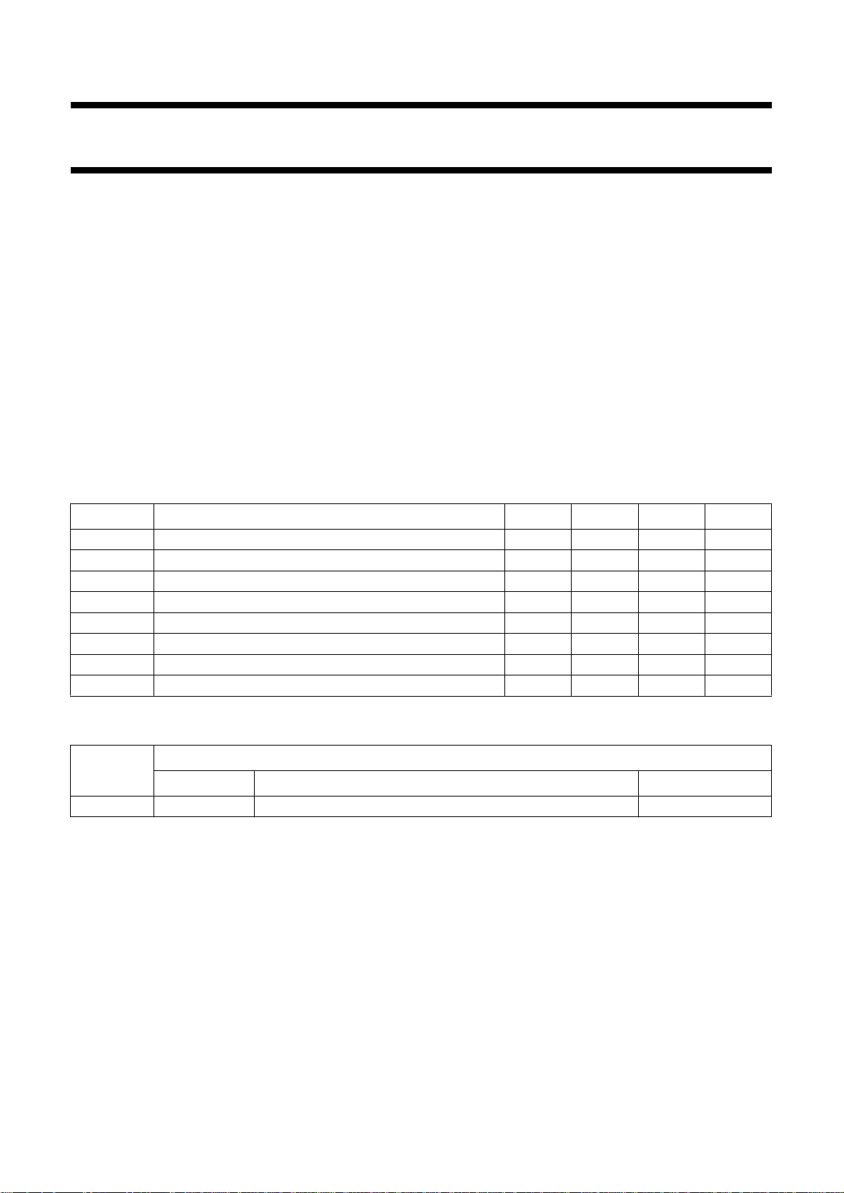
BLOCK DIAGRAM
handbook, full pagewidth
TDA4861
VOLTAGE
STABILIZER
VERTICAL
DRIVER
DIFFERENTIAL
INPUT
AMPLIFIER
THERMAL AND
SOAR
PROTECTION
VERTICAL
OUTPUT
FLYBACK
DRIVER
FLYBACK
GENERATOR
TDA4861
PULSE
CIRCUIT
V
P1
+
8.8 V
470
150 kΩ
from TDA4850
V-shift
Assumed values:
I
= 1.42A.
yoke
R
= 4.17 Ω +7%+∆R(T) =6.12 Ω.
yoke
L
= 5.25 mH.
yoke
R1= 1.0 Ω±1%.
T
=65°C.
amb
T
= 105 °C.
j(max)
T
=75°C.
yoke
P
= 1.2 W.
yoke
PIC= 1.8 W.
P
= 3.0 W.
tot
t
= typically 250 µs.
pFLB
Attention: the heatsink of the IC must be isolated against ground (it is connected to pin 6).
µF
1 MΩ
1.8 kΩ
1.8 kΩ
BAX13
270 Ω
R1
1 Ω
V-OUT SUB FLB
V
P2
5.6 Ω
0.1 µF
yoke
−
8.1 V
470 µF
V
N
470 µF
4.3 Ω
87654321 9
V
+
52 V
P3
10 kΩ
R
PCO
PCO
MHA612
Fig.1 Block diagram and application circuit with flyback supply voltage VP3 from an external source.
Deflection frequency range from 50 to 100 Hz.
1997 Jan 20 3
Philips Semiconductors Product specification
Vertical deflection power amplifier for
monitors
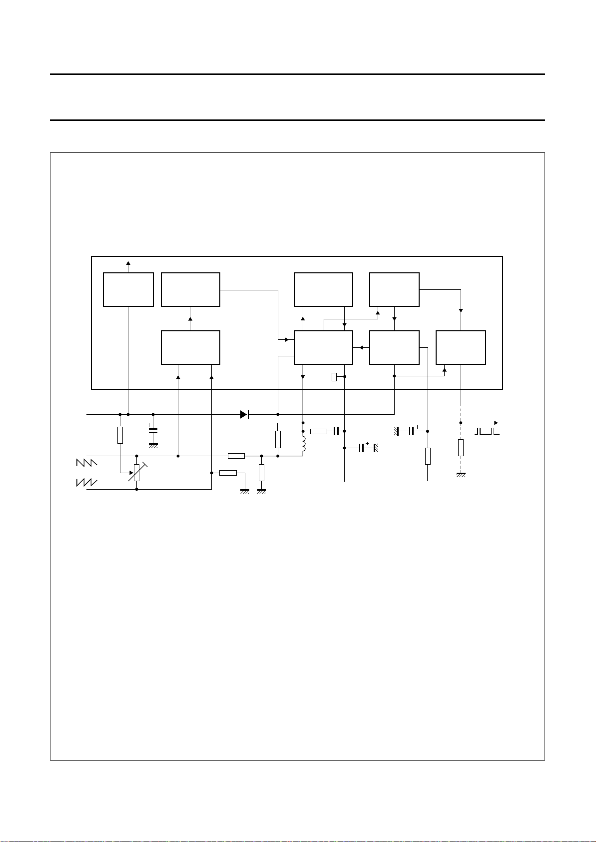
PINNING
SYMBOL PIN DESCRIPTION
V
P1
INP1 2 input 1 of differential input amplifier
INP2 3 input 2 of differential input amplifier
V
P2
V-OUT 5 vertical output
SUB 6 substrate
FLB 7 flyback generator output
V
P3
PCO 9 pulse circuit output
1 supply voltage 1
supply voltage 2 for vertical output
4
stage
8 flyback supply voltage 3
handbook, halfpage
V
1
P1
INP1
2
INP2
3
V
4
P2
V-OUT
5
TDA4861
SUB
6
7
FLB
V
8
P3
9
PCO
MEH360
Fig.2 Pin configuration.
TDA4861
FUNCTIONAL DESCRIPTION
Differential input amplifier
The differential sawtooth input signal (coming from a ramp
output of the TDA4850 for example) is fed to the input at
pins 2 and 3. The non-inverted signal is attached to pin 3.
The vertical feedback signal is superimposed on the
inverted input signal on pin 2.
Vertical shift is applied at the inputs in a power-less way
(see Fig.1).
Flyback generator
Signals for the flyback generator and the pulse circuit are
generated in the flyback driver stage. The flyback output
consists of a Darlington transistor and a flyback diode.
The flyback generator can operate in two modes:
1. An external supply voltage is applied for the short
flyback time, thus the power dissipation is minimum
(see Fig.1).
2. The flyback voltage is generated by doubling the
supply voltage (see Fig.5). The 100 µF capacitor C2
connected between pins 4 and 7 is charged up to V
P1
during scan, using the external diode and the resistor
R2. The cathode of the capacitor C2 is connected to
the positive rail during flyback. Thus, the flyback
voltage is twice the supply voltage.
Vertical output
The vertical output stage is a quasi-complementary
class-B amplifier with a high linearity. The output contains
SOAR (short-circuit protection) and thermal protection.
The output current on pin 5 is reduced for a short time
(to let the temperature decrease to Tj< 150 °C), when the
junction temperature (Tj) exceeds 160 °C.
Deflection GUARD
Pin 9 will go HIGH if the junction temperature goes too
high (see Fig.3). A pulse signal with 50% duty cycle is
output on pin 9, if the deflection coil is open-circuit.
A flyback pulse signal is output at normal conditions.
Further watching can be achieved by means of an external
GUARD circuit as shown in Fig.4. The 22 µF capacitor is
charged during flyback time (V
) at normal conditions.
5>V8
In the event of failures, the capacitor is discharged and the
GUARD output goes HIGH.
GUARD output level (see Fig.4):
• LOW for normal conditions
• HIGH for deflection coil short-circuit respectively
open-circuit
• HIGH when there are neither input or output signals.
1997 Jan 20 4

Philips Semiconductors Product specification
Vertical deflection power amplifier for
TDA4861
monitors
LIMITING VALUES
In accordance with the Absolute Maximum Rating System (IEC 134); voltages referenced to substrate (pin 6);
unless otherwise specified.
SYMBOL PARAMETER CONDITIONS MIN. MAX. UNIT
V
P1
V
P2
V
P3
V
2,3,9
V
5,7
I
4
I
5 (M)
I
7 (M)
I
9
T
stg
T
amb
T
j
V
es
supply voltage (pin 1) − 40 V
supply voltage (pin 4) − 60 V
supply voltage (pin 8) − 60 V
voltage on pins 2, 3 and 9 − V
P1
V
voltage on pins 5 and 7 − 60 V
current on pin 4 − 1A
output current on pin 5 (peak value) note 1 −±1.5 A
flyback current on pin 7 (peak value) −±1.5 A
current on pin 9 −−8mA
storage temperature −25 +150 °C
operating ambient temperature −20 +75 °C
junction temperature note 1 − 168 °C
electrostatic handling for all pins note 2 −±300 V
Notes
1. Internally limited by thermal protection; switching temperature point at 160 ±8 °C.
2. Equivalent to discharging a 200 pF capacitor through a 0 Ω series resistor.
THERMAL CHARACTERISTICS
SYMBOL PARAMETER VALUE UNIT
R
th j-mb
thermal resistance from junction to mounting base 5 K/W
The heatsink can be estimated according to application circuit (see Fig.1):
T
R
th j-a
A heatsink is needed at R
R
th h-a
R
++
th j-mbRth mb-hRth h-a
th j-mb
= 22.2 K/W − (5 + 0.5) K/W = 16.7 K/W.
j(max)Tamb
---------------------------------- P
IC(max)
< 5 K/W and R
–
th mb-h
105 °C65°C–
-----------------------------------------
1.8 W
22.2 K/W====
.
= 0.5 K/W (using silicon grease) with
1997 Jan 20 5

Philips Semiconductors Product specification
Vertical deflection power amplifier for
TDA4861
monitors
CHARACTERISTICS
VP1=VP2= 25 V; VN=V6=0V; T
SYMBOL PARAMETER CONDITIONS MIN. TYP. MAX. UNIT
V
P1
V
P2
V
P3
I
P1
I
P2
supply voltage 1 (pin 1) 9 25 30 V
supply voltage 2 (pin 4) 9 25 60 V
supply voltage 3 (pin 8) 9 − 60 V
supply current (pin 1) −−10 mA
quiescent supply current (pin 4) without input signal − 9 − mA
Pre-amplifier
V
2,3
I
2,3
input voltage (pins 2 and 3) 1.6 − VP1− 0.5 V
input quiescent current without input signal − 100 − nA
Flyback generator
V
I
7(M)
7
output voltage upper value; I7= −1A − VP3− 2.2 − V
flyback output current
(maximum value; pin 7)
V
1-5
t
pFLB
threshold voltage to switch flyback on/off threshold − 1.4 − V
flyback pulse time see Figs 1 and 3 − 250 −µs
Vertical output; see Fig.3
V
5
I
5(p-p)
output voltage upper value; I5= −1A VP2− 2.3 VP2− 2 − V
vertical output current
(peak-to-peak value; pin 5)
LIN non-linearity of output signal −−1%
=25°C; voltages referenced to substrate (pin 6); unless otherwise specified.
amb
−−±1.3 A
lower value; I
upper value;
I
= −1.4 A
5
lower value; I
=1A − 1.5 1.7 V
5
− VP2− 2.3 − V
= 1.4 A − 1.7 − V
5
−−2.8 A
Pulse circuit output; see Fig.3
V
9
output voltage R
PCO
see Fig.1
V
9
output voltage for thermal protection
active
V
1-5
t
p9
voltage to insert flyback pulse on pin 9 normal condition −−1.4 V
pulse width deflection open-circuit − 50 − %
normal condition t
1997 Jan 20 6
=10kΩ;
0.4 − VP1− 0.4 V
VP1− 0.4 −−V
pFLB
−−µs

Philips Semiconductors Product specification
Vertical deflection power amplifier for
monitors
handbook, full pagewidth
INP1
INP2
V-OUT
t
pFLB
= 250 µs
TDA4861
input signal
on pin 2
t
input signal
on pin 3
t
output signal
on pin 5
PCO
PCO
PCO
t
p9
50%
t
output signal
on pin 9 for
normal condition
t
output signal
on pin 9 for deflection
unit open-circuit
t
output signal
on pin 9 for thermal
protection active
t
MEH361
1997 Jan 20 7
Fig.3 Vertical timing.

Philips Semiconductors Product specification
Vertical deflection power amplifier for
monitors
APPLICATION INFORMATION
8
5
V
P3
vertical
output
signal
handbook, full pagewidth
TDA4861
Fig.4 GUARD circuit application on vertical output.
BAX13
2.2 Ω 3.3 kΩ
2N5819
22 µF
>1 kΩ
220 kΩ
V
P
BC548
TDA4861
GUARD output
HIGH = error
MEH362
handbook, full pagewidth
+
9 V
470
µF
from TDA4850
VOLTAGE
STABILIZER
V
P1
150 kΩ
V-shift
DIFFERENTIAL
1 MΩ
VERTICAL
DRIVER
INPUT
AMPLIFIER
1.8 kΩ
1.8 kΩ
TDA4861
BAX13
270 Ω
R1
1 Ω
THERMAL AND
SOAR
PROTECTION
VERTICAL
OUTPUT
V-OUT SUB FLB
V
P2
C2 100 µF
5.6 Ω
0.1 µF
5.25 mH
yoke
−
7.8 V
470 µF
V
GENERATOR
R2 240 Ω
N
FLYBACK
DRIVER
FLYBACK
PULSE
CIRCUIT
87654321 9
V
P3
10 kΩ
R
PCO
PCO
MEH359
Fig.5 Application for flyback voltage generation by doubling the supply voltage.
1997 Jan 20 8

Philips Semiconductors Product specification
Vertical deflection power amplifier for
monitors
handbook, full pagewidth
V
P1
12 3 657894
TDA4861
V-OUTINP2INP1
V
P2
SUB PCOV
TDA4861
P3
MHA611
Fig.6 Internal circuitry.
1997 Jan 20 9

Philips Semiconductors Product specification
Vertical deflection power amplifier for
monitors
PACKAGE OUTLINE
SIL9P: plastic single in-line power package; 9 leads
D
d
TDA4861
SOT131-2
non-concave
x
E
h
view B: mounting base side
A
B
j
D
h
2
E
seating plane
b
19
Z
DIMENSIONS (mm are the original dimensions)
A
UNIT A
mm
Note
1. Plastic or metal protrusions of 0.25 mm maximum per side are not included.
1
max.
2.0
OUTLINE
VERSION
SOT131-2
4.6
4.2
e
b
b
cD
max.
1.1
p2
0.75
0.48
0.60
0.38
IEC JEDEC EIAJ
b
p
(1)
24.0
23.6
REFERENCES
w M
0 5 10 mm
scale
deD
h
20.0
10 2.54
19.6
E
12.2
11.8
A
1
L
c
Q
(1)
E
h
6
3.4
3.1
Lj
Q
17.2
2.1
16.5
1.8
EUROPEAN
PROJECTION
0.25w0.03
ISSUE DATE
92-11-17
95-03-11
(1)
Z
x
2.00
1.45
1997 Jan 20 10

Philips Semiconductors Product specification
Vertical deflection power amplifier for
monitors
SOLDERING
Introduction
There is no soldering method that is ideal for all IC
packages. Wave soldering is often preferred when
through-hole and surface mounted components are mixed
on one printed-circuit board. However, wave soldering is
not always suitable for surface mounted ICs, or for
printed-circuits with high population densities. In these
situations reflow soldering is often used.
This text gives a very brief insight to a complex technology.
A more in-depth account of soldering ICs can be found in
“IC Package Databook”
our
Soldering by dipping or by wave
The maximum permissible temperature of the solder is
260 °C; solder at this temperature must not be in contact
with the joint for more than 5 seconds. The total contact
time of successive solder waves must not exceed
5 seconds.
(order code 9398 652 90011).
TDA4861
The device may be mounted up to the seating plane, but
the temperature of the plastic body must not exceed the
specified maximum storage temperature (T
printed-circuit board has been pre-heated, forced cooling
may be necessary immediately after soldering to keep the
temperature within the permissible limit.
Repairing soldered joints
Apply a low voltage soldering iron (less than 24 V) to the
lead(s) of the package, below the seating plane or not
more than 2 mm above it. If the temperature of the
soldering iron bit is less than 300 °C it may remain in
contact for up to 10 seconds. If the bit temperature is
between 300 and 400 °C, contact may be up to 5 seconds.
stg max
). If the
DEFINITIONS
Data sheet status
Objective specification This data sheet contains target or goal specifications for product development.
Preliminary specification This data sheet contains preliminary data; supplementary data may be published later.
Product specification This data sheet contains final product specifications.
Limiting values
Limiting values given are in accordance with the Absolute Maximum Rating System (IEC 134). Stress above one or
more of the limiting values may cause permanent damage to the device. These are stress ratings only and operation
of the device at these or at any other conditions above those given in the Characteristics sections of the specification
is not implied. Exposure to limiting values for extended periods may affect device reliability.
Application information
Where application information is given, it is advisory and does not form part of the specification.
LIFE SUPPORT APPLICATIONS
These products are not designed for use in life support appliances, devices, or systems where malfunction of these
products can reasonably be expected to result in personal injury. Philips customers using or selling these products for
use in such applications do so at their own risk and agree to fully indemnify Philips for any damages resulting from such
improper use or sale.
1997 Jan 20 11
 Loading...