

INTEGRATED CIRCUITS
DATA SH EET
TDA4800
Vertical deflection circuit for monitor
applications
Preliminary specification
File under Integrated Circuits, IC02
February 1992
Philips Semiconductors Preliminary specification
Vertical deflection circuit for monitor applications TDA4800
FEATURES
• Fully integrated, few external components
• RC oscillator with wide sync range of 1:3 (e.g. 50 Hz to
150 Hz)
• Preamplifier
• Power output stage with thermal and SOAR protection
• Flyback generator
• Internal voltage stabilizer
• Synchronization by positive or negative going sync
pulse
• Blanking pulse duration is determined externally
• Dual frequency criterion for automatic amplitude
switch-over (e.g. 50 Hz to 60 Hz)
• Guard circuit for screen protection
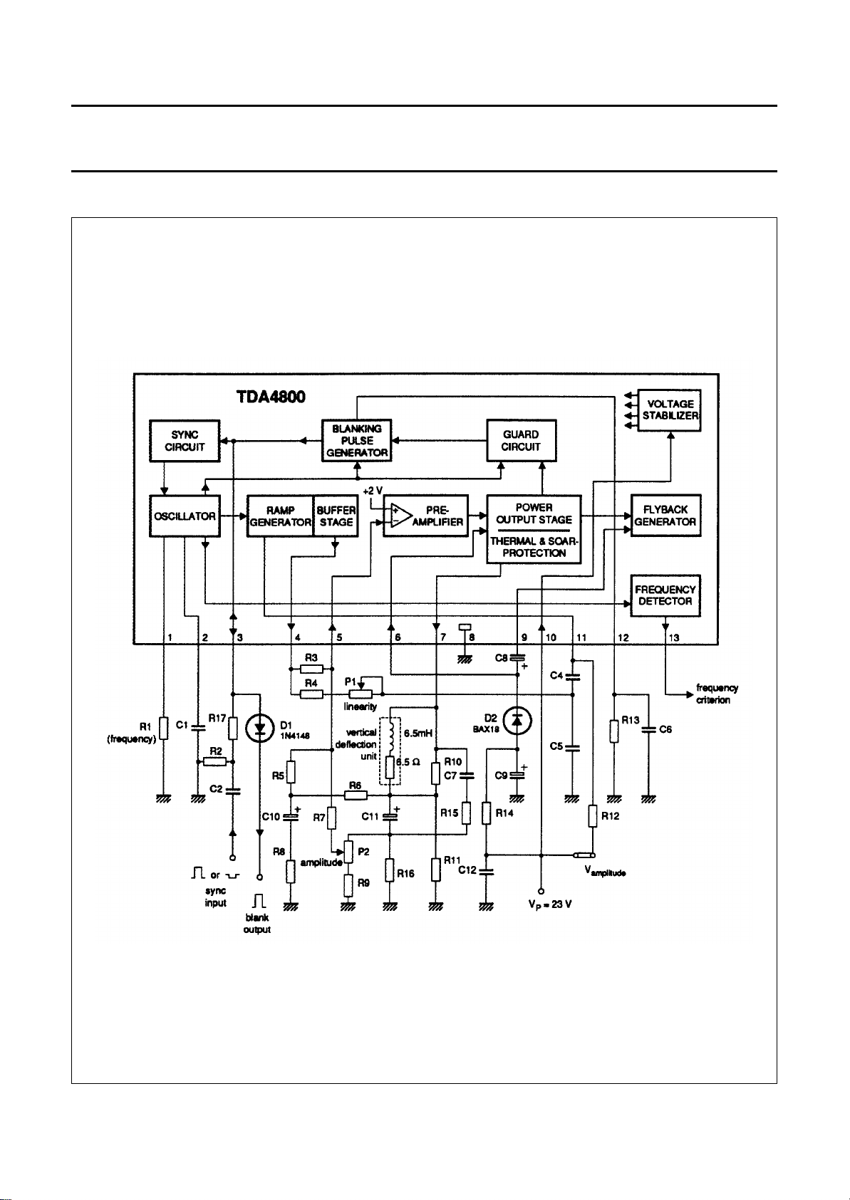
GENERAL DESCRIPTION
The TDA4800 is a monolithic integrated circuit for vertical
deflection primarily in monitors (and TV receivers). The
complete circuit consists of 11 main functional blocks as
shown in Fig.1.
• Sawtooth generator with buffer stage supplied by
external voltage
QUICK REFERENCE DATA
SYMBOL PARAMETER CONDITIONS MIN. TYP. MAX. UNIT
V
V
I
P
I
7
f
sync
V
V
T
P
P
3
3
amb
supply voltage range (pin 10) 10 − 45 V
supply voltage range (pin 6) 10 − 30 V
supply current (pins 6 and 10) note 1 − 215 − mA
output current (peak-to-peak value) −−2.6 A
picture frequency note 1, 3 −−135 Hz
positive sync input pulse 1.0 − 6.0 V
negative sync input pulse −0.5 −−0.7 V
operating ambient temperature range note 2 −20 −+70 °C
Notes to the quick reference data
1. Measured in circuit Fig.4
2. P
3. fo= 45 Hz (f
= 3.6 W for R
tot
sync max
th j−a
=3f
= 20 K/W
o)
ORDERING INFORMATION
EXTENDED
TYPE NUMBER
PACKAGE
PINS PIN POSITION MATERIAL CODE
TDA4800 13 DBS plastic SOT141
Note
1. SOT141-6; 1996 November 15.
February 1992 2
(1)
Philips Semiconductors Preliminary specification
Vertical deflection circuit for monitor applications TDA4800
BLOCK DIAGRAM
February 1992 3
Fig.1 Block diagram

Philips Semiconductors Preliminary specification
Vertical deflection circuit for monitor applications TDA4800
FUNCTIONAL DESCRIPTION
The complete circuit consists of the following functional
blocks as shown in Fig.1:
1. Oscillator
2. Synchronization circuit
3. Blanking pulse generator
4. Frequency detector and storage
5. Ramp generator
6. Buffer stage
7. Preamplifier
8. Power output stage
9. Flyback generator
10. Guard circuit
11. Voltage stabilizer
1. Oscillator (pins 1, 2)
The oscillator is an RC-oscillator with a threshold value
switch, which ensures very good frequency stability.
The upper and lower threshold voltages are defined by an
internal voltage divider.
An external capacitor C1 at pin 2 is charged by a constant
current source. When the scan voltage of C1 reaches the
upper threshold voltage, oscillator flyback starts. Capacitor
C1 discharges via an internal resistor and transistor until
the lower threshold is reached.
The constant charge current and free-running frequency
are adjusted by an external resistor R1 at pin 1:
f
o
f
o
1
-------------------------------KR1C1××
with K = 0.68=
2. Synchronization circuit (pin 3)
A positive- or negative-going pulse fed to pin 3
synchronizes the oscillator by lowering the upper threshold
voltage. The synchronizing range is f
50 Hz f
f
o
→ 150 Hz.==
sync max
to 3 fo. For example:
o
3. Blanking pulse generator (pin 3)
Also at pin 3 a blanking pulse is available. Diode D1
separates the synchronization pulse from the blanking
pulse. During scanning, the external capacitor C6 at pin 12
is charged to an internal stabilized voltage V. The blanking
pulse starts with the beginning of oscillator flyback; then
capacitor C6 discharges via the external resistor R13 at
pin 12. The blanking pulse stops when the capacitor
voltage is V/2.
The blanking pulse duration is determined by the values of
external components R13 and C6 at pin 12:
R13C6Ln2××=
t
bl
4. Frequency detector with storage (pin 13)
At the end of the scanning period a frequency detector
detects the oscillator frequency (see
Note
). When this
frequency is above the threshold a flip-flop is set to store
this information. The output is an open collector output.
Note:
Frequency detector change-over at pin 13 from low ( = low
frequency) to high ( = high frequency) is determined by fo:
f
threshold
1.23 fo×=
5. Ramp generator (pin 11)
The ramp generator consists of two external series
capacitors C4 and C5, external charge resistor R12
(connected to pin 11), and an internal differential amplifier
which is synchronously-switched by the oscillator.
External capacitors C4 and C5 at pin 11 are charged by
the charging current via the external charge resistor R12
until oscillator flyback starts. C4 and C5 are then
discharged via pin 11 by an internal resistor and transistor.
This generates a positive-going ramp voltage.
6. Buffer stage (pin 4)
The buffer stage consists of two emitter followers. The
ramp voltage is fed via the buffer stage and is available at
pin 4 with a low ohmic output impedance. With R4 and P1
it generates a ramp function, which, together with the
feedback network of the deflection yoke, gives a high
degree of linearity at the picture tube. The linearity can be
adjusted by P1.
7. Preamplifier (pin 5)
The preamplifier is a differential amplifier. The
non-inverting input is fixed at about 2 V by an internal
voltage divider. The inverting input at pin 5 is connected to
the ramp voltage via R3 and feedback network
P2, R5 - R11, R15, R16, C7, C10 and C11.
8. Power output stage (pin 7)
The power output stage is an amplifier with a
quasi-complementary class-B output. The output is
connected to pin 7.
The power stage includes SOAR and thermal protection.
February 1992 4

Philips Semiconductors Preliminary specification
Vertical deflection circuit for monitor applications TDA4800
9. Flyback generator (pin 9)
The flyback generator has an external capacitor C8 at
pin 9. During scanning, the internal circuit switches pin 9
almost to ground; thereby C8 is charged by the supply
voltage via external components R14 and D2.
During the flyback time pin 9 is switched almost to the
supply voltage, so that the supply voltage for the power
output stage (pin 6) is nearly doubled. This high flyback
voltage ensures a very short flyback time.
10. Guard circuit (pin 3)
When the vertical deflection current is absent (e.g.
short-circuit, or open-circuit of the yoke) the guard circuit
changes the blanking pulse at pin 3 into a DC signal which
blanks the beam current to protect the screen. Also an
oscillator defect (C1 short-circuited or R1 disconnected
from pin 1) switches on the guard circuit.
11. Voltage stabilizer
The voltage stabilizer circuit provides a stable operating
voltage of about 7.5 V for several circuits of the TDA4800.
February 1992 5

Philips Semiconductors Preliminary specification
Vertical deflection circuit for monitor applications TDA4800
PINNING
SYMBOL PIN DESCRIPTION
OSC
OSC
SYB
R
C
O
1 oscillator resistor
2 oscillator capacitor
3 sync. input,
blanking pulse output
S
OUT
PRE
P
SUP
I
4 sawtooth output
5 preamplifier input
6 power supply
OUTP 7 deflection output
GND 8 ground
C
FLY
9 pin for the flyback generator
capacitor
V
P
S
GEN
BP
FRQ
DU
C
10 supply voltage
11 sawtooth generator
12 blanking pulse duration
13 frequency criterion
Fig.2 Internal circuits.
Fig.3 Pin configuration.
February 1992 6

Philips Semiconductors Preliminary specification
Vertical deflection circuit for monitor applications TDA4800
LIMITING VALUES
In accordance with the Absolute Maximum System (IEC 134)
SYMBOL PARAMETER CONDITIONS MIN. MAX. UNIT
V
2
V
11
V
12
V
13
V
10
V
9
V
7
V
6
V
5
V
4
V
3
I
1
I
3
I
4
, I7,I
I
6
I
9
I
11
T
stg
T
amb
T
j max
P
tot
V
ESD
voltages 0 6 V
024V
06V
050V
supply voltages (VP) 0 50 V
050V
060V
060V
06V
024V
−0.7 6 V
currents 0 −1mA
+3 −10 mA
0 −5mA
8
see note 1
−1.5 + 1.5 A
−0.1 + 30 mA
storage temperature range −25 +150 °C
operating ambient temperature range see note 2 −20 + 70 °C
maximum junction temperature see note 3 − 150 °C
total power dissipation see note 2 −−W
ESD sensitivity see note 4 −2000 +2000 V
Notes to the limiting values
, I7and I8are limited by SOAR protection circuit that ensures that a short-circuit between the output pin 7 and supply
1. I
6
voltage or ground does not destroy the output stage. A short-circuit may be soldered into the printed-circuit board or
may sometimes (non-periodically) occur in the applied circuit.
2. The maximum value for the operating ambient temperature range and the power dissipation depends on the
heatsink.
3. Internally limited by thermal protection: switching temperature point at Tj= 150 °C ±8 °C.
4. Human body model: 1.5 kΩ, 100 pF, 5 pulses.
THERMAL RESISTANCE
SYMBOL PARAMETER THERMAL RESISTANCE
R
R
th j-a
th j-mb
from junction to ambient 20 K/W
from junction to mounting base 5 K/W
February 1992 7

Philips Semiconductors Preliminary specification
Vertical deflection circuit for monitor applications TDA4800
CHARACTERISTICS
All voltages are measured to V
GND
(pin 8); T
SYMBOL PARAMETER CONDITIONS MIN. TYP. MAX. UNIT
V
P
V
P
I
10
I
6
I
6
V
7
V
7
V
9
I
7
I
9
I
5
V
1
V
3
R
3
I
3
t
bl
V
11
I
11
V
13
I
13
V
4
I
4
V
3
V
3
supply voltage.range (pin 10) 10 − 45 V
supply voltage range (pin 6) 10 − 30 V
supply current V10= 25 V; V5=3V
supply current V6=25V; V5=1V
supply current V6=25V; V5=3V
minimum output voltage I7=1A − 1.4 1.65 V
maximum output voltage I7= −1A V6−2.3 V6−2.0 − V
output voltage during flyback I9= −1A − V10−2.2 − V
output current −−±1.3 A
output current −−±1.3 A
preamplifier input current −−0.1 −µA
stabilized voltage 6.1 6.8 7.3 V
blanking pulse output voltage − 5.7 − V
blanking pulse output resistance − 300 −Ω
blanking pulse output current 0 −−3mA
blanking pulse duration R = 100 kΩ;
output voltage ramp generator 0.3 − 20 V
output current ramp generator −2 − 15× 103µA
output voltage frequency detector lower frequency
leakage current frequency detector higher frequency
output voltage buffer stage 0 − 20 V
output current buffer stage −−−4.0 mA
synchronizing input voltage positive sync 1.0 − 6.0 V
synchronizing input voltage negative sync −0.5 −−0.7 V
tolerance of free running oscillator without sync −3.0 −+3.0 %
∆f/f / ∆TCoscillator temperature dependency T
∆f/f / ∆VPoscillator voltage dependency VP= 10 V to 30 V − 4 × 10
f0/f
sync
synchronizing ratio 1:2.9 1:3 −−
=25°C; VP= 23 V; unless otherwise specified.
amb
− 12 − mA
without load
− 20 − mA
without load
− 5 − mA
without load
640 680 730 µs
C = 10 nF (pin 12)
−−1.0 V
I13=1mA
−−1.0 µA
V13=50V
=20°C to 100 °C − 10
case
−4
−4
− K
− K
−1
−1
February 1992 8

Philips Semiconductors Preliminary specification
Vertical deflection circuit for monitor applications TDA4800
February 1992 9
Fig.4 Test and application circuit.

Philips Semiconductors Preliminary specification
Vertical deflection circuit for monitor applications TDA4800
TDA4800 IN THE TEST AND APPLICATION CIRCUIT (see Fig.4)
SYMBOL PARAMETER CONDITIONS TYP. UNIT
V
P
I
P
V
7
V
7M
I
7
I
Y(p−p)
t
fb
t
bl
P
tot
f
o
supply voltage 23 V
supply current 215 mA
DC output voltage 11.8 V
peak output voltage 45 V
output current 0.8 A
vertical deflection current (peak to peak) 1.5 A
flyback time 0.3 ms
blanking pulse duration 1.25 ms
total power dissipation 3.3 W
free running oscillator frequency without sync 45 Hz
February 1992 10

Philips Semiconductors Preliminary specification
Vertical deflection circuit for monitor applications TDA4800
PACKAGE OUTLINE
DBS13P: plastic DIL-bent-SIL power package; 13 leads (lead length 12 mm)
non-concave
x
D
E
h
view B: mounting base side
d
B
j
A
SOT141-6
D
h
2
E
A
113
e
Z
DIMENSIONS (mm are the original dimensions)
UNIT A e
mm
Note
1. Plastic or metal protrusions of 0.25 mm maximum per side are not included.
OUTLINE
VERSION
SOT141-6
A2bpcD
17.0
4.6
4.2
0.75
0.60
15.5
1
e
(1)
0.48
24.0
23.6
20.0
19.6
0.38
IEC JEDEC EIAJ
w M
b
p
0 5 10 mm
(1)
deD
E
h
12.2
10 3.4
11.8
REFERENCES
scale
1
1.7
e
5.08
L
3
L
E
2
h
6
Q
c
m
LL3m
3.4
12.4
3.1
11.0
e
2
2.4
1.6
PROJECTION
Qj
2.1
4.3
1.8
EUROPEAN
v M
v
0.8
x
0.25w0.03
ISSUE DATE
92-11-17
95-03-11
(1)
Z
2.00
1.45
February 1992 11

Philips Semiconductors Preliminary specification
Vertical deflection circuit for monitor applications TDA4800
SOLDERING
Introduction
There is no soldering method that is ideal for all IC packages. Wave soldering is often preferred when through-hole and
surface mounted components are mixed on one printed-circuit board. However, wave soldering is not always suitable for
surface mounted ICs, or for printed-circuits with high population densities. In these situations reflow soldering is often
used.
This text gives a very brief insight to a complex technology. A more in-depth account of soldering ICs can be found in our
“IC Package Databook”
Soldering by dipping or by wave
The maximum permissible temperature of the solder is 260 °C; solder at this temperature must not be in contact with the
joint for more than 5 seconds. The total contact time of successive solder waves must not exceed 5 seconds.
The device may be mounted up to the seating plane, but the temperature of the plastic body must not exceed the
specified maximum storage temperature (T
be necessary immediately after soldering to keep the temperature within the permissible limit.
(order code 9398 652 90011).
). If the printed-circuit board has been pre-heated, forced cooling may
stg max
Repairing soldered joints
Apply a low voltage soldering iron (less than 24 V) to the lead(s) of the package, below the seating plane or not more
than 2 mm above it. If the temperature of the soldering iron bit is less than 300 °C it may remain in contact for up to
10 seconds. If the bit temperature is between 300 and 400 °C, contact may be up to 5 seconds.
DEFINITIONS
Data sheet status
Objective specification This data sheet contains target or goal specifications for product development.
Preliminary specification This data sheet contains preliminary data; supplementary data may be published later.
Product specification This data sheet contains final product specifications.
Limiting values
Limiting values given are in accordance with the Absolute Maximum Rating System (IEC 134). Stress above one or
more of the limiting values may cause permanent damage to the device. These are stress ratings only and operation
of the device at these or at any other conditions above those given in the Characteristics sections of the specification
is not implied. Exposure to limiting values for extended periods may affect device reliability.
Application information
Where application information is given, it is advisory and does not form part of the specification.
LIFE SUPPORT APPLICATIONS
These products are not designed for use in life support appliances, devices, or systems where malfunction of these
products can reasonably be expected to result in personal injury. Philips customers using or selling these products for
use in such applications do so at their own risk and agree to fully indemnify Philips for any damages resulting from such
improper use or sale.
February 1992 12
 Loading...