


INTEGRATED CIRCUITS
DATA SH EET
TDA1383
DCC record/playback amplifier
Preliminary specification
File under Integrated Circuits, IC01
1995 Aug 30

Philips Semiconductors Preliminary specification
DCC record/playback amplifier TDA1383
FEATURES
General
• Single 3 V power supply
• Low standby current consumption
• Internal voltage regulator for improved supply ripple
rejection
• Double-speed DCC record and playback
• Can be applied with all generations of digital processing
ICs
• All gains and settings are software controlled
• Reduced number of external components.
Record part
• Single point main data and AUX data record current
setting
• Reduction of power consumption between current
pulses
• Accurate temperature compensation of the record
current by measuring the tape temperature
• Soft switching of record currents
• Timing compatible with TDA1319T and TDA1381H.
GENERAL DESCRIPTION
The TDA1383 is a single-chip record and playback
amplifier for a Digital Compact Cassette (DCC) tapedeck,
including Analog Compact Cassette (ACC) playback
functions. The device is designed to be used with the
Philips DCC head, type RP410R1/15. All modes of
operation and settings can be controlled by a single serial
input. Application of the TDA1383 provides a small,
versatile, low power and inexpensive DCC front-end.
Playback part
• Low noise amplifiers
• Pre-equalization and anti-aliasing filters
• Automatic gain control of DCC preamplifiers
• Optional recording of auxiliary data during DCC
playback
• Auxiliary data detect after record e.g. to detect end of
tape or ‘head clogging’
• Two amplifiers for ACC equalization
• Control signal for ferro/chrome switches
• Mute for ACC playback
• Music search function during ACC (re)wind (to be
confirmed).
ORDERING INFORMATION
TYPE
NUMBER
TDA1383H LQFP48 plastic low profile quad flat package; 48 leads; body 7 × 7 × 1.4 mm SOT313-2
NAME DESCRIPTION VERSION
PACKAGE
1995 Aug 30 2

Philips Semiconductors Preliminary specification
DCC record/playback amplifier TDA1383
QUICK REFERENCE DATA
=25°C; V
T
amb
DD1=VDD2
SYMBOL PARAMETER CONDITIONS MIN. TYP. MAX. UNIT
V
V
DD1
DD1
supply voltage 1 record part 2.7 3.3 5.5 V
supply voltage 1 record part and
playback part
V
DD2
I
DD1+IDD2
I
stb
I
D
supply voltage 2 playback part 2.7 3.3 5.5 V
supply current DCC record mode;
total standby supply current no clock; note 1 −−50 µA
record current main data
channels 0 to 7
I
AUX
record/erase current auxiliary
data channel
P
T
d(av)
amb
average power dissipation DCC record mode;
operating ambient temperature −30 − +85 °C
= 3.3 V; unless otherwise specified.
note 1 tbf 3.3 5.5 V
ID= 100 mA
DCC playback mode;
= 3 mA
I
sense
ACC playback mode;
I
= 3 mA
sense
see Table 1 10 − 125 mA
ID= 100 mA
DCC playback mode;
=3mA
I
sense
ACC playback mode;
=3mA
I
sense
− 45 60 mA
− 52 68 mA
− 29 38 mA
10 − 153 mA
− 130 − mW
− 150 − mW
− 85 − mW
Note
1. V
Table 1 Maximum record current as a function of V
is not connected to V
DD2
V
DD1
(internal voltage regulator on).
DD1
and record head resistance
DD1
R
=10Ω R
rec
2.7 V 75 90 110
3.3 V 90 110 125
>4 V 125 125 125
1995 Aug 30 3
= 6.5 Ω R
rec
rec
=4Ω
Philips Semiconductors Preliminary specification
DCC record/playback amplifier TDA1383
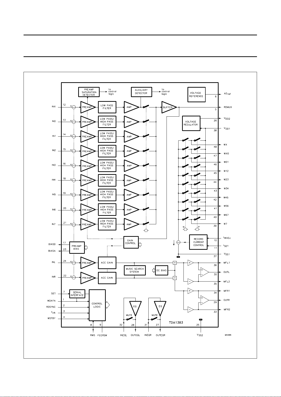
BLOCK DIAGRAM
1995 Aug 30 4
Fig.1 Block diagram.

Philips Semiconductors Preliminary specification
DCC record/playback amplifier TDA1383
PINNING
SYMBOL PIN DESCRIPTION
WDATA 1 record data input/control data input
RDSYNC 2 playback sync input
T
CLK
WSTBY 4 record standby control input
RDMUX 5 multiplexed DCC data output
AD
ref
SET 7 control data input
RWS 8 music search output/AUX detector output/saturation detector output/external clock input
FECRSW 9 ferro-chrome switch control signal
I
WADJ
I
SET
INX 12 auxiliary channel input
IN0 13 channel 0 input
IN1 14 channel 1 input
IN2 15 channel 2 input
IN3 16 channel 3 input
BIASD 17 DCC bias voltage output
IN4 18 channel 4 input
IN5 19 channel 5 input
IN6 20 channel 6 input
IN7 21 channel 7 input
INR 22 ACC right channel input
BIASA 23 ACC bias voltage output
INL 24 ACC left channel input
V
SS2
V
DD2
OUTEQR 27 right channel equalization amplifier output
OUTEQL 28 left channel equalization amplifier output
OUTR 29 right channel ACC output
OUTL 30 left channel ACC output
INEQR 31 right channel equalization amplifier input
INEQL 32 left channel equalization amplifier input
MFR2 33 right channel feedback amplifier output 2
MFR1 34 right channel feedback amplifier output 1
MFL2 35 left channel feedback amplifier output 2
MFL1 36 left channel feedback amplifier output 1
V
SS1
V
DD1
W7 39 channel 7 record current output
W67 40 channel 6/7 record current output
3 tape clock input
6 AD reference voltage output
10 record current adjust input
11 record current set input
25 ground for playback part
26 supply voltage for playback part/voltage regulator output
37 ground for record part (substrate)
38 supply voltage for record part
1995 Aug 30 5

Philips Semiconductors Preliminary specification
DCC record/playback amplifier TDA1383
SYMBOL PIN DESCRIPTION
W56 41 channel 5/6 record current output
W45 42 channel 4/5 record current output
W34 43 channel 3/4 record current output
W23 44 channel 2/3 record current output
W12 45 channel 1/2 record current output
W01 46 channel 0/1 record current output
WX0 47 channel X/0 record current output
WX 48 channel X record current output
1995 Aug 30 6
Fig.2 Pin configuration.

Philips Semiconductors Preliminary specification
DCC record/playback amplifier TDA1383
FUNCTIONAL DESCRIPTION
A brief functional description of each block (see Fig.1) is
given. The record part of the IC includes the record current
control circuit, the current source and output switches. The
DCC playback part includes nine channels, each
consisting of a preamplifier, filters and an amplifier,
automatic gain control and sense current (bias) circuits.
Differential amplifiers with presettable gain and bias are
Modes of operation
All modes and (analog) settings are digitally controlled via
the serial interface. Table 2. shows an overview of the
modes of operation and the corresponding values of the
control bits. For a number of bits it is allowed to deviate
from this table (see description of the control bits). In the
record modes additional control bits must be set, see
Table 11 and Fig.6.
used for ACC feedback to the head.
Table 2 Modes of operation
CONTROL BITS
MODE
DCC playback 0000010
DCC search 0010010 0
DCC playback and AUX
data record
DCC playback and AUX
D6D5D4D3D2D1D0S3S2S1S0G2G1G0B4B3B2B1B
(2)
0
(2)
0000010 0
DCC sense voltage
see Table 11
DCC gain
see Table 12
0110010 0
(2) (2)
(2) (2)
data detection
DCC record 0000110 −−−−−−−1−
(3)
ACC playback 0 0
ACC search 0 1 − 0011 −
Standby
(1)
0000110 −−−−−−−1−−−−
1011
ACC sense voltage
see Table 11
0 DCC gain
see
Table 12
DC bias voltage at
ACC outputs
see Table 10
0
−−−
−−−
−−
−−
(2)
−−
Notes
1. TDAPLB and TAUPLB must be set HIGH (see Table 13).
2. 0 = normal-speed; 1 = double-speed.
3. 0 = LOW level at FECRSW output; 1 = HIGH level at FECRSW output.
Serial interface
Settings of the IC can be programmed either via the SET
input pin or the WDATA input pin. When sending data via
the WDATA pin, the SET pin must be held LOW, the data
is then provided in the SET time-slot of the serial data word
(one bit per cycle of 32 clock periods, see Fig.6). Four
different control bytes are recognised (see Table 3).
The settings can be sent asynchronously at a bit-rate of
1
⁄32f
(96 kbits/s in case of normal speed). The data
Tclk
transfer must be preceeded by a start bit (LOW) and end
with a stop bit (HIGH), as shown in Fig.3. The SET data
detector starts at the falling edge of the start bit. Each
control bit is detected in the middle. After power-up at least
ten stop bits (320 clock periods) must be sent in order to
initialize the serial interface.
Fig.3 Timing diagram of the SET byte.
1995 Aug 30 7
Philips Semiconductors Preliminary specification
DCC record/playback amplifier TDA1383
Table 3 Control bytes
CONTROL BYTE BIT 0 BIT 1 BIT 2 BIT 3 BIT 4 BIT 5 BIT 6 BIT 7
Byte 1 0 0 D0 D1 D2 D3 D4 D5
Byte 2 1 0 D6 − S0 S1 S2 S3
Byte 3 0 1 −−−G1 G1 G2
Byte 4 1 1 − B0 B1 B3 B3 B4
Description of the control bits
Tables 4 to 12 describe the functions of the various control
bits.
The magneto-resistive playback head (MRH) is directly
connected to the IC. Bits D3 to D1 control the internal
Table 4 Control bit D0
D0 MODE
0 DCC playback/record
1 ACC playback
Table 5 Control bits D2 and D1
D2 D1 FUNCTION
0 0 preamp input floating, second stages
normal (for testing only)
0 1 cut-off frequencies normal
1 0 cut-off frequencies high
1 1 cut-off frequencies very high (standby, fast
settling)
Table 8 Detector modes and outputs
AC coupling to the MRH and DC biasing of capacitors
connected between the internal amplifiers (see Fig.9).
The cut-off frequencies are related to the clock frequency
at T
or RWS (bit D3). Higher clock frequencies will result
clk
in higher cut-off frequencies.
Table 6 Control bit D3
D3 FUNCTION
0 cut-off frequencies coupled to the frequency at
T
(pin 3)
clk
1 cut-off frequencies coupled to the frequency at
RWS (pin 8)
Table 7 Control bit D4
D4 DCC MODE (D0 = 0) ACC MODE (D0 = 1)
0 AGC on FECRSW = LOW level
(pin 9)
1 AGC off, gain setting
at G2, G1 and G0
FECRSW = HIGH level
(pin 9)
D5
(1)
D6
FUNCTION IN ACC MODE
0 0 music search detector off AUX detector off control frequency input
0 1 test preamp saturation level test preamp saturation level saturation level detector output
1 0 music search detector on AUX detector on filtered MSS and AUX detector
1 1 music search detector on AUX detector on (direct MSS and AUX detector
Note
1. D3 and D5 should not be at logic 1 at the same time.
1995 Aug 30 8
(D0=1)
FUNCTION IN DCC MODE
(D0=0)
PIN RWS (see Fig.9)
(HIGH when saturated)
output
output, for testing only)
Philips Semiconductors Preliminary specification
DCC record/playback amplifier TDA1383
Table 9 Control bits B4 to B2
BIT VALUE FUNCTION IN DCC MODE (D0 = 0) FUNCTION IN ACC MODE (D0 = 1)
(1)
B4
B3 0 filters set for playback at normal-speed
B2 0 recording at normal-speed
Note
1. The bit B4 determines the sign of feedback bias voltage. If B4 = 0 then MFL1 and MFR1 are negative with respect
to MFL2 and MFR2. If B4 = 1 then MFL1 and MFR1 are positive with respect to MFL2 and MFR2.
Table 10 Feedback conductor bias voltage settings in the ACC mode (D0 = 1, no MRH connected)
0 playback mode on
1 playback mode off
1 filters set for playback at double-speed
1 recording at double-speed
see Table 10
BIAS VOLTAGE BIT
B3 B2 B1 B0
00 0 0 0
00 0 1 30
00 1 0 60
00 1 1 90
0 1 0 0 120
0 1 0 1 150
0 1 1 0 180
0 1 1 1 210
1 0 0 0 240
1 0 0 1 270
1 0 1 0 300
1 0 1 1 330
1 1 0 0 360
1 1 0 1 390
1 1 1 0 420
1 1 1 1 450
TYPICAL DC BIAS VOLTAGE (mV)
1995 Aug 30 9

Philips Semiconductors Preliminary specification
DCC record/playback amplifier TDA1383
Table 11 Sense voltage settings with DCC heads of 50 Ω and ACC heads of 200 Ω connected
SENSE VOLTAGE BITS
S3 S2 S1 S0
0 0 0 0 50 80
0 0 0 1 80 160
0010 110 230
0 0 1 1 140 310
0 1 0 0 170 390
0 1 0 1 200 470
0 1 1 0 230 550
0 1 1 1 260 630
1 0 0 0 290 700
1 0 0 1 320 780
1 0 1 0 350 860
1 0 1 1 380 940
1 1 0 0 410 1020
1 1 0 1 440 1090
1 1 1 0 470 1170
1 1 1 1 500 1250
(1)
TYPICAL DCC SENSE VOLTAGE
(D0 = 0; B4 = 0)
(2)
TYPICAL ACC SENSE VOLTAGE
(D0=1)
(2)
Notes
1. Bits S3 to S0 control the sense voltage at the preamp input pins in both DCC and ACC mode. The sense current can
be calculated from the sense voltage and the MRH resistance.
2. Depends on V
DD1
and V
, if no saturation occurs.
DD2
Table 12 Gain settings
GAIN SET BITS
(1)
G2 G1 G0
DCC MODE; AGC OFF (D0 = 0; D4 = 1) ACC MODE (D0 = 1; D3 = 1)
DCC GAIN AT 50 kHz TYPICAL (dB) (PIN 5)
MAIN DATA (dB) AUX DATA (dB)
ACC GAIN AT 1 kHz TYPICAL (dB)
(PINS 29 AND 30)
0 0 0 70 52.5 50.5 equalizer operational
0 0 1 71.7 54.2 54.5
amplifier active
0 1 0 72.3 55.8 58.5
0 1 1 75 57.5 62.5
1 0 0 76.6 59.1 50.5 equalizer operational
1 0 1 78.3 60.8 54.5
amplifier mute
1 1 0 79.9 62.4 58.5
1 1 1 81.6 64.1 62.5
Note
1. In the ACC mode G2 controls the mute switch over the equalizer operational amplifier (switch closed when G2 = 1).
1995 Aug 30 10

Philips Semiconductors Preliminary specification
DCC record/playback amplifier TDA1383
DCC record
The TDA1383 record part is designed to drive the
elements of a nine-channel integrated record head.
ECORD CURRENT CONTROL
R
The record current at the outputs is regulated by the
current control circuit. The principle of this circuit is shown
in Fig.4.
The value of the main data record current ID can be set by
applying a voltage to pin 10. This voltage can be derived
from the reference voltage output at pin 6.
During AUX data record (outputs WX and WX0 active) the
output current (IX) is increased by a factor AW. During the
erase mode of the auxiliary channel (TERAUX = HIGH,
see Table 2), the output current ID is increased by a
factor AE.
ECORD MODES
R
Recording is controlled by the 32-bit wide serial data word
which is clocked in at WDATA (pin 1). The current pulses
are made available at the outputs WX to W7.
The timing sequence of the current pulses is shown in
Fig.6. The operating mode of the record part can be set by
the first three bits of the WDATA word. The signals
TCH0 to TCH7 and TCHAUX determine the direction of
the record current. When TCH
is HIGH, the current flows
i
as indicated in Fig.5. Otherwise current flows in the
opposite direction. The principle of connection of the
record head to the IC is also illustrated in Fig.5. The
various modes of operation are given in Table 13. The
standby mode can also be forced by setting the WSTBY
input (pin 4) HIGH.
RECORD CURRENT OUTPUTS
Each channel is selected in sequence. Depending on the
data bit (TCH0 to TCHAUX), the current is directed
forward or reverse through the heads. The outputs that are
not selected are kept floating to prevent any incorrect
current flow. Current flow through a channel of the
recording head is achieved by closing one of the switches
P and the switch N of an adjacent channel (see Fig.1).
Table 13 DCC record modes
MODE RECORD CURRENT CONTROL BIT
MAIN DA TA
CHANNELS
AUX
CHANNEL
MAIN DATA
CHANNELS
AUX
CHANNEL
TDAPLB
(DATA CHANNEL
PLAYBACK)
record part STANDBY off off 1
record playback I
record record I
record erase I
D
D
D
playback record off A
playback erase off A
off 0
AW× I
D
AE× I
D
× I
W
D
× I
E
D
(2)
TAUPLB
(AUX CHANNEL
PLA YBACK)
(1)
(1)
000
001
100
101
(2)
TERAUX
(AUX CHANNEL
ERASE)
1X
(1)
1X
Notes
1. 0 = LOW, 1 = HIGH and X = don't care.
2. When both TDAPLB and TAUPLB are HIGH, the record part of the IC is set to the standby mode. AW and AE are
multiplication factors (see current control).
1995 Aug 30 11

Philips Semiconductors Preliminary specification
DCC record/playback amplifier TDA1383
Fig.4 Principle of the record current control circuit.
1995 Aug 30 12
Fig.5 Definition of record currents.

Philips Semiconductors Preliminary specification
DCC record/playback amplifier TDA1383
(1) Erase pulses are inverted every other cycle of 32 clock pulses.
Fig.6 Timing diagram of record current pulses.
RECORD STANDBY MODE
The record circuit is set to the standby mode when
TDAPLB = 1 and TAUPLB = 1 (see Table 13), or when a
HIGH level is applied to WSTBY (pin 4). TDAPLB and
TAUPLB will be overruled by a HIGH level on WSTBY.
After a HIGH-to-LOW transition at WSTBY, the circuit will
remain in the standby mode, until TDAPLB = 0 or
TAUPLB = 0.
RECORD CURRENT TEMPERATURE COMPENSATION
During recording a fixed current is directed through the
right channel ACC playback head. The resulting voltage
over the head is temperature dependent and is used for
compensation of the record current. This method ensures
optimum record current at any tape temperature
(see Fig.4).
1995 Aug 30 13

Philips Semiconductors Preliminary specification
DCC record/playback amplifier TDA1383
DCC playback
PREAMPLIFIERS, FILTERS, MULTIPLEXERS AND OUTPUT
BUFFER
The TDA1383 has nine low-noise preamplifiers, which are
connected to a nine-channel magneto-resistive head
(MRH). The heads must be DC-coupled to the IC. The
preamplifiers will provide the necessary biasing
conditions. Eight of the nine channels are for the DCC
main data, the other is for the auxiliary (AUX) data. The
eight main data channels have pre-equalization for
frequencies from 1 to 50 kHz (1st-order highpass, −3dB
at 75 kHz), and a lowpass filter for anti-aliasing (2nd-order
active, −3 dB at 120 kHz). The auxiliary data channel has
a flat frequency response (from 100 Hz to 100 kHz).
A multiplexing circuit switches the nine digital channels
sequentially to the output RDMUX. The AUX data is
sampled during two clock periods, the eight main data
channels are sampled during one clock period. The
effective sample frequency is one tenth of the clock
frequency at T
OUBLE-SPEED
D
(see Fig.8).
clk
The IC can be set to double speed DCC playback by
setting bit B3 to logic 1 and applying a 6.144 MHz clock
frequency. In this case all poles of the pre-equalization and
anti-aliasing filters will be multiplied by a factor of two.
UTOMATIC GAIN CONTROL
A
SAA2032, SAA2023 or SAA3323). There is a fixed
relationship between decay time and recovery time of the
preamplifier gain (t
times t
). The AGC is active only in the DCC mode and
decay
is approximately equal to ten
recovery
can be switched off by setting D4 to logic 1. In this
condition a fixed gain can be set via the serial input
(see Table 12).
ENSE CURRENT
S
Separate, adjustable low-noise voltage sources are
available at the inputs to provide the sense currents
through the MRH. The voltage levels are controlled by the
sense voltage bits, see Table 11. The principle of the
sense voltage sources is shown in Fig.9. The value of the
sense current is determined by the applied sense voltage
and the MRH resistance. When the current through the
MRH is too high, the input transistor will be saturated. This
is detected by the saturation detector, which produces a
HIGH output if Vc drops below Vb. Saturation is detected at
the inputs INX and IN7. The detector output (available at
pin 8) will become HIGH if one of the inputs INX or IN7 is
saturated.
UXILIARY DATA DETECTOR
A
A detector is available to detect the AUX signal envelope
immediately after writing AUX data. This feature can be
used to detect end of tape or head clogging. The output is
available on pin 8 and will become HIGH if the AUX
amplitude on RDMUX is above the specified level.
The DCC part is equipped with an automatic gain control
circuit (AGC) which decreases the gain of the
preamplifiers when the level at RDMUX exceeds a preset
value. In this way an optimum voltage swing at the
RDMUX output is obtained (for the ADC input of SAA2051,
1995 Aug 30 14
UXILIARY DATA RECORD DURING DCC PLAYBACK
A
Provides possibility to write or erase auxiliary data.

Philips Semiconductors Preliminary specification
BB
DCC record/playback amplifier TDA1383
Fig.7 Typical gain of the main data and auxiliary data channel (AGC off, gain set to maximum).
1995 Aug 30 15
Fig.8 Timing diagram of read signals.

Philips Semiconductors Preliminary specification
DCC record/playback amplifier TDA1383
Fig.9 Principle of the sense voltage sources and the RWS output.
ACC playback
REAMPLIFIER
P
The ACC playback MRH's are also directly connected to
the inputs INL and INR. The preamplifier provides an
adjustable sense voltage in order to bias the heads, in the
same way as for the DCC inputs. Saturation is also
checked on both input stages. Input signals are amplified
in two stages. The gain can be set with bits G1 and G0
(see Table 12). The left and right outputs are available at
pins 30 and 29.
EEDBACK AMPLIFIERS
F
Separate ACC output stages are capable of driving a
conductor in the MRH. This conductor will provide
magnetic feedback to the head, in order to improve the
linearity of the analog audio response. The left and right
feedback signals are available at the outputs MFL1, MFL2
and MFR1, MFR2. The feedback amplifiers are also used
for DC biasing of the feedback conductors of the MRH.
A presettable DC level is added to the amplified signals
before the output drivers. The DC bias voltage over the
feedback conductor can be set by the control bits B4 to B0
(Table 10). This will result in a DC bias current through the
head.
EQUALIZATION AMPLIFIERS
Two uncommitted operational amplifiers are available for
pre-equalization of the left and right ACC signals. These
amplifiers operate only during ACC playback. The
non-inverting input is internally connected to a DC voltage
approximately equal to 1.25 V. The equalization amplifier
outputs can be muted via the serial interface, bit G2.
Muting is achieved by closing an internal switch between
output and inverting input. It is advised to connect the
output to the input if the amplifier is not used in the
application.
SWITCH CONTROL SIGNAL
Fe/Cr
A control signal is available for setting the de-emphasis
time constant switch from ferro to chrome (Fe/Cr) type in
an application circuit. The signal is available at pin 9 and is
HIGH when control bit D4 is set to logic 1.
1995 Aug 30 16

Philips Semiconductors Preliminary specification
DCC record/playback amplifier TDA1383
MUSIC SEARCH SYSTEM (MSS)
This IC is equiped with a music detector which can be
enabled via the serial interface (bit D5 = 1). This circuit can
be used to find empty spaces between recordings during
high-speed search. The ACC outputs (pins 29, 30 and
33 to 36) are muted when the music detector is active. The
output of the MSS (pin 8) will go HIGH if a signal is
detected. Remark; To be confirmed.
INPUT (PIN 8)
RWS
When bit D3 is set to logic 1 pin 8 will become input for the
signal whose frequency controls the cross-over
frequencies of the internal AC couplings between the head
and the preamplifier (used in ACC mode only).
General
NTERNAL STABILIZATION
I
The internal voltage regulator stabilises the supply voltage
V
of the playback part, including amplifiers, filters and
DD2
voltage references. The circuit requires a small voltage
drop between input and output for optimum operation.
The regulator can be switched off by connecting V
V
. Figure 10 shows the typical ripple rejection of the
DD1
DD2
to
regulator. C26 is a decoupling capacitor between
pin 26 and pin 25.
OLTAGE REFERENCES
V
The DC output voltage AD
bandgap reference voltage source. AD
is derived from an internal
ref
(referenced to
ref
VSS) can be used as reference voltage for analog-to-digital
conversion of the RDMUX output. When the AGC is active
the signal at RDMUX will not exceed the DC level of AD
AD
can also be used for the adjustment of the record
ref
ref
current (see Fig.4).
TANDBY MODE
S
When the IC is in the standby mode
(see Tables 2 and 13), all circuits are switched off to
minimize the power consumption, all record current
outputs are floating, and the voltage reference output is
switched off. During power-up WSTBY must be high in
order to prevent unwanted record current pulses.
.
(1) C26 = 1 µF.
(2) C26 = 10 µF.
1995 Aug 30 17
Fig.10 Ripple rejection of the voltage regulator (typ.).

Philips Semiconductors Preliminary specification
DCC record/playback amplifier TDA1383
LIMITING VALUES
In accordance with the Absolute Maximum Rating System (IEC 134). All voltages are referenced to V
(pins 25 and 37 externally tied together), currents positive into the IC.
SYMBOL PARAMETER CONDITIONS MIN. MAX. UNIT
V
DD1
V
DD2
V
i
I
26,38(max)
I
39-48(max)
supply voltage 1 record part −0.3 +5.5 V
supply voltage 2 playback part −0.3 +5.5 V
input voltage VDD+ 0.3 < 5.5 V −0.3 VDD+ 0.3 V
maximum input current supply (pins 26 and 38) −200 +200 mA
maximum input current record output
−200 +200 mA
(pins 39 to 48)
I
33-36(max)
maximum input current ACC feedback output
−80 +80 mA
(pins 33 to 36)
I
n(max)
P
tot
T
amb
T
stg
V
es
maximum input current remaining pins −10 +10 mA
total power dissipation − 600 mW
operating ambient temperature −30 +85 °C
storage temperature −55 +150 °C
electrostatic handling note 1 −3000 +3000 V
note 2 −300 +300 V
SS1
and V
SS2
Notes
1. Human body model: equivalent to discharging a 100 pF capacitor through a 1.5 kΩ series resistor.
2. Machine model: equivalent to discharging a 200 pF capacitor through a 25 Ω series resistor and a 2.5 µH series
inductor.
QUALITY SPECIFICATION
In accordance with SNW-FQ-661 part E. The numbers of the quality specification can be found in the
Handbook”
. The handbook can be ordered using the code 9398 510 63011.
“Quality Reference
THERMAL CHARACTERISTICS
SYMBOL PARAMETER VALUE UNIT
R
th j-a
thermal resistance from junction to ambient in free air 65 K/W
1995 Aug 30 18

Philips Semiconductors Preliminary specification
DCC record/playback amplifier TDA1383
CHARACTERISTICS
Voltages referenced to VSS (pins 25 and 37, tied together externally); currents positive into the IC; supply voltage
V
DD2=VDD1
T
= +25 °C; f
amb
SYMBOL PARAMETER CONDITIONS MIN. TYP. MAX. UNIT
Supplies
V
DD1
V
DD1
V
DD2
V
DD1−VDD2
I
DD1+IDD2
I
stb
P
d(av)
AD
ref
DIGITAL INPUTS (PINS 1 TO 4, 7 AND 8)
V
IH
V
IL
I
LI
t
su
t
hd
t
r
t
f
DIGITAL OUTPUT (PIN 8)
V
OH
V
OL
= 3.3 V (pins 26 and 38); internal voltage regulator off; test circuit in accordance with Fig.12;
= 3.072 MHz; settings in accordance with Table 2; unless otherwise specified.
Tclk
supply voltage 1 record part,
2.7 3.3 5.5 V
FB part and logic part
supply voltage 1 record part voltage regulator used tbf 3.3 5.5 V
supply voltage 2 playback part 2.7 3.3 5.5 V
voltage drop over regulator voltage regulator used;
V
= 3.3 V
DD1
supply current DCC record mode;
0.45 0.6 0.75 V
− 45 60 mA
ID= 100 mA
DCC playback mode;
=3mA
I
sense
ACC playback mode;
=3mA
I
sense
total standby current voltage regulator on;
− 52 68 mA
− 33 45 mA
−−50 µA
no clock
average power dissipation DCC record mode;
− 150 − mW
ID= 100 mA
DCC playback mode;
=3mA
I
sense
ACC playback mode;
=3mA
I
sense
− 170 − mW
− 110 − mW
reference voltage output D0 = 0 1.9 2.0 2.15 V
HIGH level input voltage 0.7V
DD1
LOW level input voltage 0 − 0.3V
− V
DD1
DD1
input leakage current −10 0 +10 µA
set-up time WDATA, RDSYNC see Fig.11 20 −− ns
hold time WDATA, RDSYNC see Fig.11 20 −− ns
rise time of tape clock see Fig.11 −−20 ns
fall time of tape clock see Fig.11 −−20 ns
HIGH level output voltage Io= −1mA V
− 0.5 − V
DD1
DD1
LOW level output voltage Io=1mA 0 − 0.5 V
V
V
V
1995 Aug 30 19

Philips Semiconductors Preliminary specification
DCC record/playback amplifier TDA1383
SYMBOL PARAMETER CONDITIONS MIN. TYP. MAX. UNIT
DCC record part
I
D
recording current main data
channels 0 to 7
I
AUX
recording current auxiliary data
channel
A
W
relative AUX data record current
increase with respect to I
A
E
relative AUX erase current
increase with respect to I
∆I
D
deviation among main data
channel currents
t
rec
rise time of record current pulse ID= 100 mA; 10% to 90%;
DCC playback part (note 2)
V
N
preamplifier input referred noise
voltage
∆V
N
3 × standard deviation of input
referred noise voltage
THD preamplifier total harmonic
distortion at TESTMUX (pin 9)
G
G
∆G
∆G
G
AUX
50
10
300
ds100
auxiliary data gain at RDMUX fi= 9.6 kHz 62 64 66 dB
main data gain at RDMUX fi= 50 kHz 78 81 84 dB
relative gain at 10 kHz fi= 10 kHz −14 −12 −10 dB
relative gain at 300 kHz fi= 300 kHz −−14 − dB
main data gain at double-speed
playback
∆G
ds20
relative gain at 20 kHz at
double-speed playback
V
o(rms)
maximum output voltage at
RDMUX (RMS value)
V
DC(RDMUX)
∆V
DC(os)
DC voltage level at RDMUX 1.05 1.15 1.25 V
DC offset voltage between
sampled outputs
V
L
lower AGC detection level at
RDMUX
V
H
upper AGC detection level at
RDMUX
V
hys
hysteresis in AGC voltage
detection level
AGC
α
cs
V
sense
cr
AGC range D4 = 0 9 11 13 dB
channel separation 30 −− dB
sense voltage (INX to IN7) R
D
D
see Table 1 10 − 125 mA
10 − 153 mA
ID= 100 mA 1.0 1.2 1.4 dB
ID= 100 mA − 3.5 − dB
ID= 100 mA; note 1 −−0.5 dB
− 36 − ns
f
= 6 MHz
Tclk
fi= 50 kHz;
R
=50Ω;
source
I
=3mA
sense
fi= 50 kHz;
R
=50Ω;
source
I
=3mA
sense
V
= 0.2 mV (RMS);
i
− 1.8 − nV/√Hz
− 0.4 − nV/√Hz
− tbf −40 dB
fi= 9.6 kHz
fi= 100 kHz 75 78 81 dB
fi= 20 kHz −12 −10 −8dB
fi= 9.6 kHz 0.5 −− V
−−200 mV
− 0.5 − V
− 1.8 − V
− 0.15 0.25 V
=50Ω 70 − 250 mV
head
1995 Aug 30 20

Philips Semiconductors Preliminary specification
DCC record/playback amplifier TDA1383
SYMBOL PARAMETER CONDITIONS MIN. TYP. MAX. UNIT
I
sense
V
AUXdet(M)
ACC playback part (note 4)
V
N
∆V
N
G
ACC
V
o(rms)
I
o(rms)
V
DC(FB)
V
os(FB)
α
cs
V
sense
I
sense(max)
V
MSS
A
mute
V
oEQ(rms)
sense current (INX to IN7) V
= maximum;
sense
−−5mA
no saturation
AUX detector voltage level at
note 3 tbf 75 tbf mV
input INX (peak voltage)
preamplifier input referred noise
voltage
3 × standard deviation of input
referred noise voltage
fi= 10 kHz;
R
= 200 Ω;
head
I
=3mA
sense
fi= 10 kHz;
R
= 200 Ω;
head
I
=3mA
sense
− 3.5 − nV/√Hz
− 1 − nV/√Hz
ACC gain at pins 29 and 30 fi= 50 to 20 kHz 60 62.5 65 dB
maximum output voltage
(RMS value) (pins 29 and 30)
fi= 1 kHz; THD < −40 dB;
RL ≥ 5kΩ; maximum gain
500 −− mV
setting = 300
maximum output current at FB
outputs (RMS value)
fi= 1 kHz; THD < −35 dB;
V
= 0; maximum gain
DC(FB)
25 −− mA
setting = 300
DC bias voltage at FB outputs no head connected;
−450 − +450 mV
see Table 10
DC offset voltage at FB outputs V
=0 −−25 mV
DC(FB)
channel separation fi= 10 kHz 40 −− dB
input sense voltage at
R
= 200 Ω 0.08 − 0.9 V
head
INL and INR
maximum input sense current at
−−4.5 mA
INL and INR
music search system detector
level
referenced to 500 mV
(RMS) at pins 29 and 30;
− 40 − dB
notes 5 and 6
equalizer output attenuation
fi= 1 kHz 30 35 − dB
during mute
maximum output voltage at
pins 27 and 28 (RMS value)
fi= 1 kHz; THD < −40 dB;
RL≥ 2.5 kΩ
0.5 −− V
Notes
1. Defined as 20log (I
2. DCC mode; AGC off; gain set to maximum (D0 = 0; D4 = 1; G2 = G1 = G0 = 1).
3. Pin 8 will become HIGH if AUX data with frequency above 1 kHz is above the specified level for longer than 10 ms.
4. ACC playback mode; D0 = 1; ACC gain set to maximum (G1 = G0 = 1); fi= 48 kHz at pin 8; bit D3 = 1; unless
otherwise specified.
5. D3 = 0; D5 = 1; D6 = 0; pin 8 will become HIGH when both channels are below this level for more than 10 ms.
6. All references to the music search system has the status ‘to be confirmed’.
1995 Aug 30 21
D(max)/ID(min)
) for channels 0 to 7.

Philips Semiconductors Preliminary specification
DCC record/playback amplifier TDA1383
Fig.11 Timing relationship between the edges of T
and WDATA.
clk
1995 Aug 30 22

Philips Semiconductors Preliminary specification
DCC record/playback amplifier TDA1383
TEST AND APPLICATION INFORMATION
1995 Aug 30 23
Fig.12 Test circuit.

Philips Semiconductors Preliminary specification
DCC record/playback amplifier TDA1383
The TDA1383 can be set to the test mode by setting
control bit D6 to logic 1. In the test mode the FECRSW
output (pin 9) is connected to a test multiplexer which
allows the low-pass filter output of each DCC channel to be
monitored (see Fig.13). The test multiplexer runs in phase
with the channel output multiplexer.
When a DC level is applied to pin 9, the emitter follower
can be turned off, allowing input to the high-pass filter. The
DC level to be applied must be 0.7 V higher than the
measured DC level of the selected channel.
Fig.13 Principle of the TESTMUX input/output.
1995 Aug 30 24

Philips Semiconductors Preliminary specification
DCC record/playback amplifier TDA1383
PACKAGE OUTLINE
LQFP48: plastic low profile quad flat package; 48 leads; body 7 x 7 x 1.4 mm
c
y
X
36
37
pin 1 index
48
25
Z
24
E
e
w
b
p
A
H
E
E
M
A
2
A
13
SOT313-2
Q
(A )
A
1
L
3
θ
L
p
1
e
w
b
p
D
H
D
12
Z
M
D
v
M
B
v
M
0 2.5 5 mm
scale
DIMENSIONS (mm are the original dimensions)
UNIT
mm
A
A1A2A3b
max.
0.20
1.60
0.05
1.45
1.35
0.25
cE
p
0.27
0.18
0.17
0.12
(1)
(1) (1)(1)
D
7.1
6.9
eH
H
7.1
6.9
0.5
9.15
8.85
Note
1. Plastic or metal protrusions of 0.25 mm maximum per side are not included.
OUTLINE
VERSION
IEC JEDEC EIAJ
REFERENCES
SOT313-2
D
A
B
9.15
8.85
detail X
LLpQZywv θ
E
0.69
0.75
0.45
0.59
0.12 0.10.21.0
EUROPEAN
PROJECTION
Z
D
0.95
0.95
0.55
0.55
ISSUE DATE
E
o
7
o
0
93-06-15
94-12-19
1995 Aug 30 25

Philips Semiconductors Preliminary specification
DCC record/playback amplifier TDA1383
SOLDERING
Introduction
There is no soldering method that is ideal for all IC
packages. Wave soldering is often preferred when
through-hole and surface mounted components are mixed
on one printed-circuit board. However, wave soldering is
not always suitable for surface mounted ICs, or for
printed-circuits with high population densities. In these
situations reflow soldering is often used.
This text gives a very brief insight to a complex technology.
A more in-depth account of soldering ICs can be found in
“IC Package Databook”
our
Reflow soldering
Reflow soldering techniques are suitable for all QFP
packages.
The choice of heating method may be influenced by larger
plastic QFP packages (44 leads, or more). If infrared or
vapour phase heating is used and the large packages are
not absolutely dry (less than 0.1% moisture content by
weight), vaporization of the small amount of moisture in
them can cause cracking of the plastic body. For more
information, refer to the Drypack chapter in our
Reference Handbook”
Reflow soldering requires solder paste (a suspension of
fine solder particles, flux and binding agent) to be applied
to the printed-circuit board by screen printing, stencilling or
pressure-syringe dispensing before package placement.
Several techniques exist for reflowing; for example,
thermal conduction by heated belt. Dwell times vary
between 50 and 300 seconds depending on heating
method. Typical reflow temperatures range from
215 to 250 °C.
Preheating is necessary to dry the paste and evaporate
the binding agent. Preheating duration: 45 minutes at
45 °C.
(order code 9398 652 90011).
“Quality
(order code 9398 510 63011).
Wave soldering
Wave soldering is not recommended for QFP packages.
This is because of the likelihood of solder bridging due to
closely-spaced leads and the possibility of incomplete
solder penetration in multi-lead devices.
If wave soldering cannot be avoided, the following
conditions must be observed:
• A double-wave (a turbulent wave with high upward
pressure followed by a smooth laminar wave)
soldering technique should be used.
• The footprint must be at an angle of 45° to the board
direction and must incorporate solder thieves
downstream and at the side corners.
Even with these conditions, do not consider wave
soldering the following packages: QFP52 (SOT379-1),
QFP100 (SOT317-1), QFP100 (SOT317-2),
QFP100 (SOT382-1) or QFP160 (SOT322-1).
During placement and before soldering, the package must
be fixed with a droplet of adhesive. The adhesive can be
applied by screen printing, pin transfer or syringe
dispensing. The package can be soldered after the
adhesive is cured.
Maximum permissible solder temperature is 260 °C, and
maximum duration of package immersion in solder is
10 seconds, if cooled to less than 150 °C within
6 seconds. Typical dwell time is 4 seconds at 250 °C.
A mildly-activated flux will eliminate the need for removal
of corrosive residues in most applications.
Repairing soldered joints
Fix the component by first soldering two diagonallyopposite end leads. Use only a low voltage soldering iron
(less than 24 V) applied to the flat part of the lead. Contact
time must be limited to 10 seconds at up to 300 °C. When
using a dedicated tool, all other leads can be soldered in
one operation within 2 to 5 seconds between
270 and 320 °C.
1995 Aug 30 26

Philips Semiconductors Preliminary specification
DCC record/playback amplifier TDA1383
DEFINITIONS
Data sheet status
Objective specification This data sheet contains target or goal specifications for product development.
Preliminary specification This data sheet contains preliminary data; supplementary data may be published later.
Product specification This data sheet contains final product specifications.
Limiting values
Limiting values given are in accordance with the Absolute Maximum Rating System (IEC 134). Stress above one or
more of the limiting values may cause permanent damage to the device. These are stress ratings only and operation
of the device at these or at any other conditions above those given in the Characteristics sections of the specification
is not implied. Exposure to limiting values for extended periods may affect device reliability.
Application information
Where application information is given, it is advisory and does not form part of the specification.
LIFE SUPPORT APPLICATIONS
These products are not designed for use in life support appliances, devices, or systems where malfunction of these
products can reasonably be expected to result in personal injury. Philips customers using or selling these products for
use in such applications do so at their own risk and agree to fully indemnify Philips for any damages resulting from such
improper use or sale.
The Digital Compact Cassette logo is a registered trade mark of Philips Electronics N.V.
1995 Aug 30 27

Philips Semiconductors – a worldwide company
Argentina: IEROD, Av. Juramento 1992 - 14.b, (1428)
BUENOS AIRES, Tel. (541)786 7633, Fax. (541)786 9367
Australia: 34 Waterloo Road, NORTH RYDE, NSW 2113,
Tel. (02)805 4455, Fax. (02)805 4466
Austria: Triester Str. 64, A-1101 WIEN, P.O. Box 213,
Tel. (01)60 101-1236, Fax. (01)60 101-1211
Belgium: Postbus 90050, 5600 PB EINDHOVEN, The Netherlands,
Tel. (31)40 783 749, Fax. (31)40 788 399
Brazil: Rua do Rocio 220 - 5
CEP: 04552-903-SÃO PAULO-SP, Brazil.
P.O. Box 7383 (01064-970),
Tel. (011)821-2333, Fax. (011)829-1849
Canada: PHILIPS SEMICONDUCTORS/COMPONENTS:
Tel. (800) 234-7381, Fax. (708) 296-8556
Chile: Av. Santa Maria 0760, SANTIAGO,
Tel. (02)773 816, Fax. (02)777 6730
China/Hong Kong: 501 Hong Kong Industrial Technology Centre,
72 Tat Chee Avenue, Kowloon Tong, HONG KONG,
Tel. (852)2319 7888, Fax. (852)2319 7700
Colombia: IPRELENSO LTDA, Carrera 21 No. 56-17,
77621 BOGOTA, Tel. (571)249 7624/(571)217 4609,
Fax. (571)217 4549
Denmark: Prags Boulevard 80, PB 1919, DK-2300
COPENHAGEN S, Tel. (032)88 2636, Fax. (031)57 1949
Finland: Sinikalliontie 3, FIN-02630 ESPOO,
Tel. (358)0-615 800, Fax. (358)0-61580 920
France: 4 Rue du Port-aux-Vins, BP317,
92156 SURESNES Cedex,
Tel. (01)4099 6161, Fax. (01)4099 6427
Germany: P.O. Box 10 63 23, 20043 HAMBURG,
Tel. (040)3296-0, Fax. (040)3296 213.
Greece: No. 15, 25th March Street, GR 17778 TAVROS,
Tel. (01)4894 339/4894 911, Fax. (01)4814 240
India: Philips INDIA Ltd, Shivsagar Estate, A Block,
Dr. Annie Besant Rd. Worli, Bombay 400 018
Tel. (022)4938 541, Fax. (022)4938 722
Indonesia: Philips House, Jalan H.R. Rasuna Said Kav. 3-4,
P.O. Box 4252, JAKARTA 12950,
Tel. (021)5201 122, Fax. (021)5205 189
Ireland: Newstead, Clonskeagh, DUBLIN 14,
Tel. (01)7640 000, Fax. (01)7640 200
Italy: PHILIPS SEMICONDUCTORS S.r.l.,
Piazza IV Novembre 3, 20124 MILANO,
Tel. (0039)2 6752 2531, Fax. (0039)2 6752 2557
Japan: Philips Bldg 13-37, Kohnan 2-chome, Minato-ku, TOKYO 108,
Tel. (03)3740 5130, Fax. (03)3740 5077
Korea: Philips House, 260-199 Itaewon-dong,
Yongsan-ku, SEOUL, Tel. (02)709-1412, Fax. (02)709-1415
Malaysia: No. 76 Jalan Universiti, 46200 PETALING JAYA,
SELANGOR, Tel. (03)750 5214, Fax. (03)757 4880
Mexico: 5900 Gateway East, Suite 200, EL PASO, TX 79905,
Tel. 9-5(800)234-7381, Fax. (708)296-8556
th
floor, Suite 51,
Netherlands: Postbus 90050, 5600 PB EINDHOVEN, Bldg. VB,
Tel. (040)783749, Fax. (040)788399
(From 10-10-1995: Tel. (040)2783749, Fax. (040)2788399)
New Zealand: 2 Wagener Place, C.P.O. Box 1041, AUCKLAND,
Tel. (09)849-4160, Fax. (09)849-7811
Norway: Box 1, Manglerud 0612, OSLO,
Tel. (022)74 8000, Fax. (022)74 8341
Pakistan: Philips Electrical Industries of Pakistan Ltd.,
Exchange Bldg. ST-2/A, Block 9, KDA Scheme 5, Clifton,
KARACHI 75600, Tel. (021)587 4641-49,
Fax. (021)577035/5874546
Philippines: PHILIPS SEMICONDUCTORS PHILIPPINES Inc,
106 Valero St. Salcedo Village, P.O. Box 2108 MCC, MAKATI,
Metro MANILA, Tel. (02)810 0161, Fax. (02)817 3474
Portugal: PHILIPS PORTUGUESA, S.A.,
Rua dr. António Loureiro Borges 5, Arquiparque - Miraflores,
Apartado 300, 2795 LINDA-A-VELHA,
Tel. (01)4163160/4163333, Fax. (01)4163174/4163366
Singapore: Lorong 1, Toa Payoh, SINGAPORE 1231,
Tel. (65)350 2000, Fax. (65)251 6500
South Africa: S.A. PHILIPS Pty Ltd.,
195-215 Main Road Martindale, 2092 JOHANNESBURG,
P.O. Box 7430, Johannesburg 2000,
Tel. (011)470-5911, Fax. (011)470-5494.
Spain: Balmes 22, 08007 BARCELONA,
Tel. (03)301 6312, Fax. (03)301 42 43
Sweden: Kottbygatan 7, Akalla. S-164 85 STOCKHOLM,
Tel. (0)8-632 2000, Fax. (0)8-632 2745
Switzerland: Allmendstrasse 140, CH-8027 ZÜRICH,
Tel. (01)488 2211, Fax. (01)481 77 30
Taiwan: PHILIPS TAIWAN Ltd., 23-30F, 66, Chung Hsiao West
Road, Sec. 1. Taipeh, Taiwan ROC, P.O. Box 22978,
TAIPEI 100, Tel. (02)388 7666, Fax. (02)382 4382
Thailand: PHILIPS ELECTRONICS (THAILAND) Ltd.,
209/2 Sanpavuth-Bangna Road Prakanong,
Bangkok 10260, THAILAND,
Tel. (662)398-0141, Fax. (662)398-3319
Turkey:Talatpasa Cad. No. 5, 80640 GÜLTEPE/ISTANBUL,
Tel. (0212)279 27 70, Fax. (0212)282 67 07
United Kingdom: Philips Semiconductors LTD.,
276 Bath Road, Hayes, MIDDLESEX UB3 5BX,
Tel. (0181)730-5000, Fax. (0181)754-8421
United States:811 East Arques Avenue, SUNNYVALE,
CA 94088-3409, Tel. (800)234-7381, Fax. (708)296-8556
Uruguay: Coronel Mora 433, MONTEVIDEO,
Tel. (02)70-4044, Fax. (02)92 0601
Internet: http://www.semiconductors.philips.com/ps/
For all other countries apply to: Philips Semiconductors,
International Marketing and Sales, Building BE-p,
P.O. Box 218, 5600 MD EINDHOVEN, The Netherlands,
Telex 35000 phtcnl, Fax. +31-40-724825 (from 10-10-1995: +31-40-2724825)
SCD41 © Philips Electronics N.V. 1995
All rights are reserved. Reproduction in whole or in part is prohibited without the
prior written consent of the copyright owner.
The information presented in this document does not form part of any quotation
or contract, is believed to be accurate and reliable and may be changed without
notice. No liability will be accepted by the publisher for any consequence of its
use. Publication thereof does not convey nor imply any license under patent- or
other industrial or intellectual property rights.
Printed in The Netherlands
513061/1500/01/pp28 Date of release: 1995 Aug 30
Document order number: 9397 750 00284
 Loading...