

INTEGRATED CIRCUITS
DATA SH EET
TDA1319T
DCC write amplifier (write 2)
Preliminary specification
File under Integrated Circuits, IC01
April 1994
Philips Semiconductors Preliminary specification
DCC write amplifier (write 2) TDA1319T
FEATURES
• Bidirectional high current output
drivers
• Single point current setting
• Extra erase current for the auxiliary
channel
• Increased current for auxiliary data
• Low standby power consumption
• Short-circuit protection to ground
• Serial data input
GENERAL DESCRIPTION
The TDA1319T has been designed to
drive an inductive recording head
which is suitable for DCC (Digital
Compact Cassette) systems.
The bidirectional current outputs are
controlled by a two-wire serial bus.
The amplitude of the write current can
be set using an external resistor. The
circuit can be switched to the standby
mode to minimize supply current
consumption.
• Reduced RF emission due to slope
control of write current.
QUICK REFERENCE DATA
SYMBOL PARAMETER CONDITIONS MIN. TYP. MAX. UNIT
V
V
I
DD
I
DDO
DD
DDO
supply voltage 4.75 5.0 5.5 V
supply voltage (write outputs) 4.75 5.0 5.5 V
supply current note 1 − 7.5 11 mA
supply current (write outputs) note 2 −−255 mA
note 3 −−365 mA
note 4 −−285 mA
I
sb
T
amb
total standby current note 5 − 23mA
operating ambient temperature −30 − +85 °C
Notes
1. 1 kΩ erase adjust resistor connected between pins 5 and 6, no load at pin 9.
2. Momentary maximum value during write data; see Table 1; IO= 225 mA.
3. Momentary maximum value during erase AUX; see Table 1 and Fig.5; resistor Re connected between pins 5 and 6
(see Fig.7).
4. Momentary maximum value during write AUX; see Table 1; IO= 255 mA.
5. Standby mode; see Table 1; Isb=IDD+I
DDO+Iclamp
.
ORDERING INFORMATION
EXTENDED TYPE
NUMBER
PINS PIN POSITION MATERIAL CODE
PACKAGE
TDA1319T 24 SO24L plastic SOT137-1
April 1994 2
Philips Semiconductors Preliminary specification
DCC write amplifier (write 2) TDA1319T
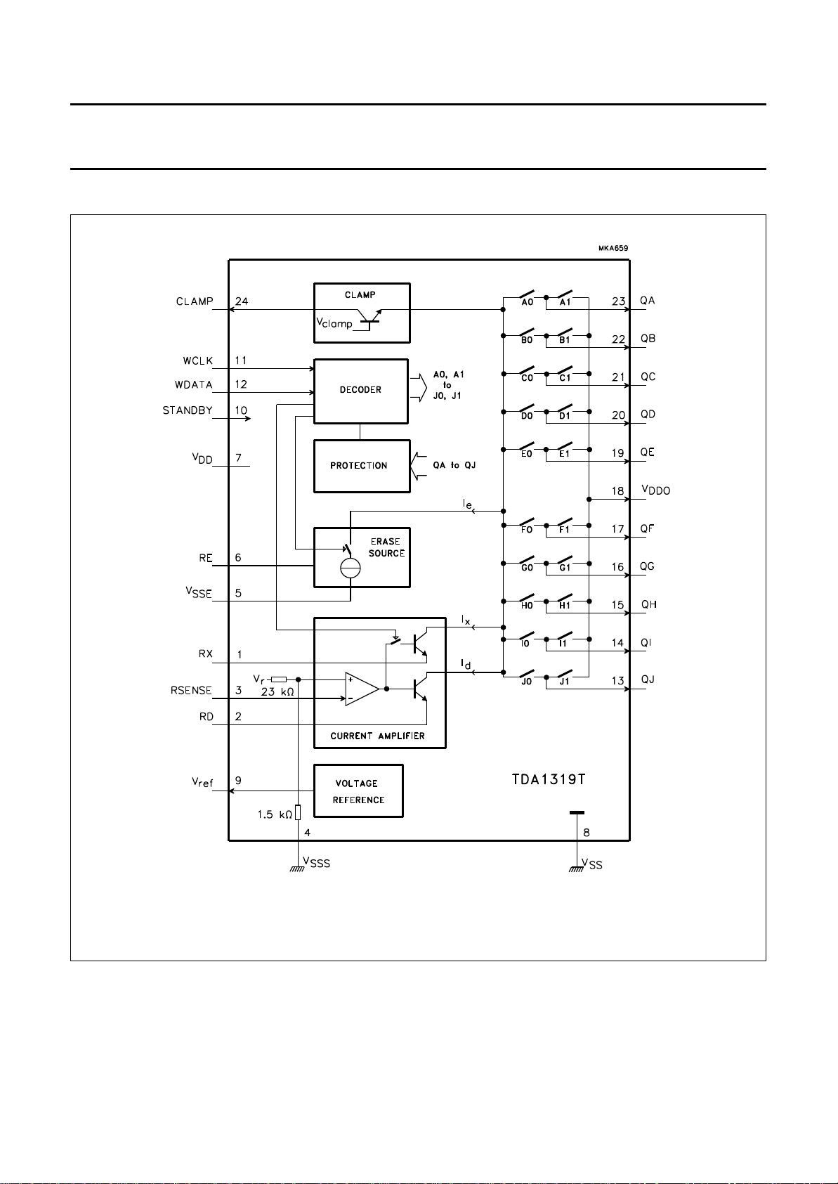
BLOCK DIAGRAM
April 1994 3
Fig.1 Block diagram.
Philips Semiconductors Preliminary specification
DCC write amplifier (write 2) TDA1319T
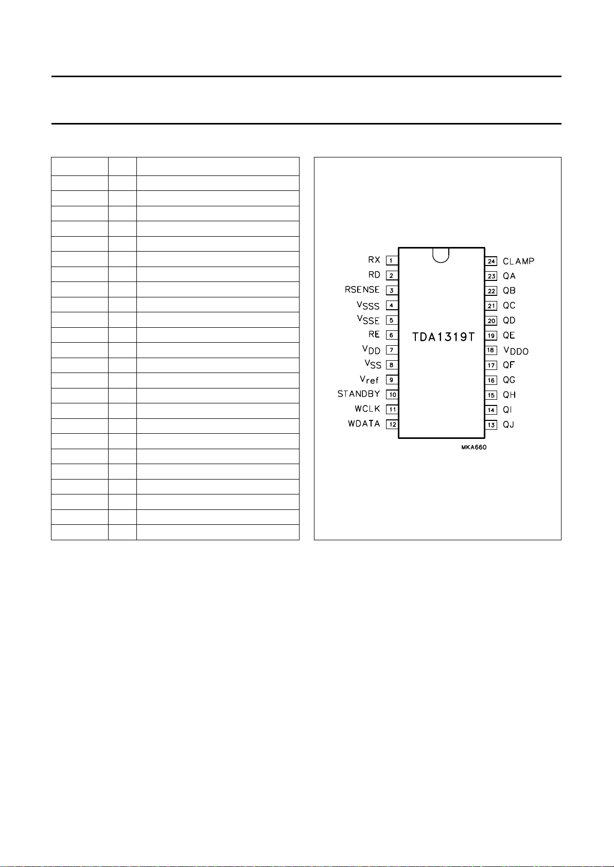
PINNING
SYMBOL PIN DESCRIPTION
RX 1 auxiliary current adjust resistor
RD 2 data current adjust resistor
RSENSE
V
SSS
V
SSE
RE 6 erase current adjust resistor
V
DD
V
SS
V
ref
STANDBY 10 standby mode control input
WCLK 11 write clock input
WDATA 12 write data input
QJ 13 write pulse output
QI 14 write pulse output
QH 15 write pulse output
QG 16 write pulse output
QF 17 write pulse output
V
DDO
QE 19 write pulse output
QD 20 write pulse output
QC 21 write pulse output
QB 22 write pulse output
QA 23 write pulse output
CLAMP 24 clamp current output
3 sense voltage positive input
4 sense voltage ground
5 erase current source ground
7 supply voltage
8 ground
9 reference voltage output
18 supply voltage (write outputs)
Fig.2 Pin configuration.
April 1994 4

Philips Semiconductors Preliminary specification
DCC write amplifier (write 2) TDA1319T
FUNCTIONAL DESCRIPTION
The TDA1319T is designed to drive the nine elements of
the multichannel recording head (as used in a DCC
recorder) by forcing a current through the selected path. A
brief functional description of each block (see Fig.1) is
given below.
Decoder
The IC is controlled by the 32-bit wide serial dataword
which is clocked in at WDATA (pin 12). The clock
frequency (WCLK, pin 11) is 3.072 MHz with a clock
period of 325 ns. The write pulses are made available at
the outputs QA to QJ (see Fig.4). The timing sequence of
the write pulses is illustrated in Fig.5.
The operating mode of the IC can be set by the first 3 bits
of data (see Fig.5). The signals TCH0 to TCH7 and
TERAUX determine the direction of the write current.
When TCHn is HIGH, the current flows as indicated in
Fig.4. When TCHn is LOW current flows in the opposite
direction. The various modes of operation are given in
Table 1. The standby mode can also be forced by setting
the STANDBY input (pin 10) HIGH.
Current amplifier
The write current at the outputs is regulated by the current
amplifier. The value of the current I
external resistor Rd, connected between pin 2 and V
can be set using an
d
SS
(see Fig.9). The current through Rd also flows at the
outputs. The current amplifier regulates the voltage across
Rd, which is measured between RSENSE and V
SSS
(pins 3 and 4), to a value of 150 mV (see Chapter
“Characteristics”). This force-sense technique eliminates
the influence of parasitic series impedances.
The output of the current amplifier is internally switched to
the output pins QA to QJ. During AUX write (outputs QA
and QB active) an additional current Ix is added to the write
current. This current can be controlled by a resistor R
x
connected between RX (pin 1) and VSS. RX must be
6.7 × Rd for 1.2 dB current increase.
During the erase mode of the auxiliary channel
(TERAUX = HIGH; see Table 1) it is possible to let an
additional output current Ie flow through QA and QB
(pins 23 and 22). This extra current can be adjusted with
an external resistor Re connected between pins 6 and 5.
Pin 5 must be externally connected to ground. A typical
value of the extra current can be calculated from the
response curve of Fig.7.
Voltage reference
A reference voltage is available at pin 9. This voltage is
derived from a bandgap reference source and can be used
to modify the voltage sensed by the current amplifier, e.g.
for external temperature compensation.
Outputs
Each channel is selected in sequence. Depending on the
dataword, the current is directed forward or reversed
through the heads. The outputs that are not selected are
kept floating to prevent any incorrect current flow. A
simplified schematic of one output stage is illustrated in
Fig.3. In the HIGH state (one of the switches A1 to J1 is
closed) the output is internally connected to a fixed voltage
(see Chapter “Characteristics”). In the LOW state
V
OH
(one of the switches A0 to J0 is closed) the output is
connected to the current amplifier. The voltage developed
across the output pin pairs must not exceed a certain
value, otherwise the lower switch transistor (Fig.3) will
become saturated.
Clamp circuit
During the periods that the head elements are not
selected, the clamp circuit accommodates the write
current. This current is directed through an external
resistor from pin 24 to the supply, in order to have less
dissipation in the IC. The clamping results in a constant
current being drawn from the supply and therefore reduces
emission of interferences (the DC level at pin 24 must not
fall lower than 1.8 V).
Standby
The circuit is in the standby mode when TDAPLB = 1 and
TAUPLB = 1 (see Table 1 and Fig.6), or when a HIGH
level is applied to pin 10. After a HIGH-to-LOW transition
at pin 10, the IC will remain in the standby mode until
TDAPLB = 0 or TAUPLB = 0. When the IC is in the
standby mode, the current amplifier is switched off to
minimize the power consumption, switches A to J are
open-circuit and the voltage reference and the erase
source are switched off.
Protection
The IC is immediately switched to standby mode when a
short-circuit to ground at an output pin is detected
< 0.5 V; see Fig.6, “SHORT”). When the short-circuit
(V
o
condition is removed, the IC will resume operation. The
state of the decoder is not affected by a “SHORT”.
April 1994 5

Philips Semiconductors Preliminary specification
DCC write amplifier (write 2) TDA1319T
Table 1 Modes of operation.
CONTROL BITS
DATA
CHANNELS
0 TO 7
AUXILIARY
CHANNELS
TDAPLB
(DATA
CHANNEL
PLAYBACK)
TAUPLB
(AUXILIARY
CHANNEL
PLAYBACK)
Read read 1 1 X standby mode
Write (Id) read 0 1 X
Write (I
Write (I
Read write (I
Read erase (I
) write (Id + Ix)0 0 0
d
) erase (Id + Ix + Ie)0 0 1
d
+ Ix)1 0 0
d
+ Ix + Ie)1 0 1
d
Note
1. X = don't care; 0 = LOW; 1 = HIGH.
(1)
TERAUX
(AUXILIARY
CHANNEL
ERASE)
REMARKS
Fig.3 Simplified schematic of ONE output stage. Fig.4 Output current definition.
April 1994 6

Philips Semiconductors Preliminary specification
DCC write amplifier (write 2) TDA1319T
April 1994 7
Fig.5 Data format and timing sequence of write pulse.
(1) Erase pulses are inverted every other cycle of 32 clock pulses.

Philips Semiconductors Preliminary specification
DCC write amplifier (write 2) TDA1319T
April 1994 8
Fig.6 Timing of the standby mode (via WDATA, STANDBY or “SHORT”).

Philips Semiconductors Preliminary specification
DCC write amplifier (write 2) TDA1319T
Fig.7 Additional erase current as a function of Re (typ.).
LIMITING VALUES
In accordance with the Absolute Maximum Rating System (IEC 134); all voltages referenced to ground (pin 8); all
currents are positive into the IC.
SYMBOL PARAMETER CONDITIONS MIN. MAX. UNIT
V
V
V
DD
DDO
I
supply voltage −0.3 +5.5 V
supply voltage (write outputs) −0.3 +5.5 V
input voltage (pins 1 to 6, 9 to 17
VDD+ 0.3 < 5.5 V −0.3 VDD+ 0.3 V
and 19 to 24)
I
n
maximum input current (pins 3, 4, 6
−10 +10 mA
and 9 to 12)
I
1
I
5
I
2
I
18
T
amb
T
stg
V
es
maximum input current (pin 1) −40 +40 mA
maximum input current (pin 5) −100 +40 mA
maximum input current (pin 2) −250 +40 mA
maximum input current (pin 18) −40 +400 mA
operating ambient temperature −30 +85 °C
storage temperature −55 +150 °C
electrostatic handling note 1 −2000 +2000 V
Note
1. Equivalent to discharging a 100 pF capacitor through a 1.5 kΩ series resistor.
THERMAL RESISTANCE
SYMBOL PARAMETER THERMAL RESISTANCE
R
th j-a
from junction to ambient in free air 65 K/W
April 1994 9

Philips Semiconductors Preliminary specification
DCC write amplifier (write 2) TDA1319T
CHARACTERISTICS
V
DD=VDDO
= 5 V; f
accordance with Fig.9; all voltages referenced to V
SYMBOL PARAMETER CONDITIONS MIN. TYP. MAX. UNIT
Supply
V
DD
V
DDO
I
DD
I
DDO
I
sb
P
d(av)
Digital inputs (pins 10 to 12)
V
IH
V
IL
I
IL
t
su
t
h
Outputs (pins 9, 13 to 17 and 19 to 23)
V
ODATH
V
OAUXH
I
O(min)
I
ODAT(max)
I
OAUX(max)
∆I
O/IO
I
AUX
I
e
V
ref
Current amplifier (pins 1 to 4)
V
sense
, V
V
1
2
= 3.072 MHz; T
clk
=25°C; outputs QA to QJ resistively loaded; resistors connected in
amb
(pin 8); unless otherwise specified..
SS
supply voltage 4.75 5.0 5.5 V
supply voltage (write outputs) 4.75 5.0 5.5 V
supply current note 1 − 7.5 11 mA
supply current (write outputs) note 2 −−255 mA
note 3 −−365 mA
note 4 −−285 mA
total standby current note 5 − 23mA
average power dissipation note 6 − 645 − mW
HIGH level input voltage 3.5 − 5.0 V
LOW level input voltage 0 − 1.5 V
input leakage current −10 − +10 µA
WDATA set-up time see Fig.8 30 −− ns
WDATA hold time see Fig.8 30 −− ns
HIGH level data output voltage note 7 − 3.7 − V
HIGH level auxiliary output voltage note 8 − 3.7 − V
minimum output current −−25 mA
maximum data output current 225 −− mA
maximum auxiliary output current note 9 335 −− mA
output current deviation between channels note 7 −−0.5 dB
relative auxiliary write current increase note 10 1 1.2 1.4 dB
additional output current note 3 −−80 mA
reference voltage (pin 9) IO< 3 mA 2.4 2.5 2.6 V
sense voltage regulation between pins 3 and 4 140 150 160 mV
maximum DC voltage level (pins 1 and 2) −−500 mV
April 1994 10

Philips Semiconductors Preliminary specification
DCC write amplifier (write 2) TDA1319T
Notes
1. 1 kΩ erase adjust resistor connected between pins 5 and 6, no load at pin 9.
2. Momentary maximum value during write data; see Table 1; IO= 225 mA.
3. Momentary maximum value during erase AUX; see Table 1 and Fig.5; resistor Re connected between pins 5 and 6
(see Fig.7).
4. Momentary maximum value during write AUX; see Table 1; IO= 255 mA.
5. Standby mode; see Table 1; Isb=IDD+I
DDO+Iclamp
6. Auxiliary and data write mode; Id= 170 mA; RL=3Ω (between current outputs); R
7. Data channels (pins 13 to 17 and 19 to 22); maximum output load resistance is 5 Ω; IO= 225 mA. Deviation defined
as 20log {(I
O(max)
− I
O(min)
)/I
} for channels 0 to 7.
o(av)
8. Auxiliary channel (pins 22 and 23); auxiliary erase mode; IO= 335 mA.
9. Auxiliary channel (pins 22 and 23); auxiliary erase mode; maximum output load resistance is 4 Ω.
10. Defined as 20log {(Id+Ix)/Id} when Rx= 6.7 × Rd.
.
=12Ω.
clamp
Fig.8 Timing relationship between the edges of WCLK and WDATA.
April 1994 11

Philips Semiconductors Preliminary specification
DCC write amplifier (write 2) TDA1319T
TEST AND APPLICATION INFORMATION
April 1994 12
Fig.9 Test circuit.

Philips Semiconductors Preliminary specification
DCC write amplifier (write 2) TDA1319T
April 1994 13
Fig.10 Application circuit.

Philips Semiconductors Preliminary specification
DCC write amplifier (write 2) TDA1319T
PACKAGE OUTLINE
handbook, full pagewidth
S
pin 1
index
112
0.9
0.4
(4x)
15.6
15.2
1.27
0.49
0.36
0.1 S
1324
0.25 M
(24x)
2.45
2.25
0.3
0.1
10.65
10.00
detail A
7.6
7.4
1.1
0.5
1.1
1.0
0.32
0.23
0 to 8
MBC235 - 1
A
2.65
2.35
o
Dimensions in mm.
Fig.11 24-lead small-outline; plastic (SOT137-1).
April 1994 14

Philips Semiconductors Preliminary specification
DCC write amplifier (write 2) TDA1319T
SOLDERING
Plastic small-outline packages
YWAVE
B
During placement and before soldering, the component
must be fixed with a droplet of adhesive. After curing the
adhesive, the component can be soldered. The adhesive
can be applied by screen printing, pin transfer or syringe
dispensing.
Maximum permissible solder temperature is 260 °C, and
maximum duration of package immersion in solder bath is
10 s, if allowed to cool to less than 150 °C within 6 s.
Typical dwell time is 4 s at 250 °C.
A modified wave soldering technique is recommended
using two solder waves (dual-wave), in which a turbulent
wave with high upward pressure is followed by a smooth
laminar wave. Using a mildly-activated flux eliminates the
need for removal of corrosive residues in most
applications.
Y SOLDER PASTE REFLOW
B
Reflow soldering requires the solder paste (a suspension
of fine solder particles, flux and binding agent) to be
applied to the substrate by screen printing, stencilling or
pressure-syringe dispensing before device placement.
Several techniques exist for reflowing; for example,
thermal conduction by heated belt, infrared, and
vapour-phase reflow. Dwell times vary between 50 and
300 s according to method. Typical reflow temperatures
range from 215 to 250 °C.
Preheating is necessary to dry the paste and evaporate
the binding agent. Preheating duration: 45 min at 45 °C.
EPAIRING SOLDERED JOINTS (BY HAND-HELD SOLDERING
R
IRON OR PULSE
-HEATED SOLDER TOOL)
Fix the component by first soldering two, diagonally
opposite, end pins. Apply the heating tool to the flat part of
the pin only. Contact time must be limited to 10 s at up to
300 °C. When using proper tools, all other pins can be
soldered in one operation within 2 to 5 s at between 270
and 320 °C. (Pulse-heated soldering is not recommended
for SO packages.)
For pulse-heated solder tool (resistance) soldering of VSO
packages, solder is applied to the substrate by dipping or
by an extra thick tin/lead plating before package
placement.
DEFINITIONS
Data sheet status
Objective specification This data sheet contains target or goal specifications for product development.
Preliminary specification This data sheet contains preliminary data; supplementary data may be published later.
Product specification This data sheet contains final product specifications.
Limiting values
Limiting values given are in accordance with the Absolute Maximum Rating System (IEC 134). Stress above one or
more of the limiting values may cause permanent damage to the device. These are stress ratings only and operation
of the device at these or at any other conditions above those given in the Characteristics sections of the specification
is not implied. Exposure to limiting values for extended periods may affect device reliability.
Application information
Where application information is given, it is advisory and does not form part of the specification.
LIFE SUPPORT APPLICATIONS
These products are not designed for use in life support appliances, devices, or systems where malfunction of these
products can reasonably be expected to result in personal injury. Philips customers using or selling these products for
use in such applications do so at their own risk and agree to fully indemnify Philips for any damages resulting from such
improper use or sale.
April 1994 15
 Loading...