


INTEGRATED CIRCUITS
DATA SH EET
SAA4996H
Motion Adaptive Colour Plus And
Control IC (MACPACIC) for
PALplus
Preliminary specification
File under Integrated Circuits, IC02
1996 Oct 28

Philips Semiconductors Preliminary specification
Motion Adaptive Colour Plus And
Control IC (MACPACIC) for PALplus
CONTENTS
1 FEATURES
2 GENERAL DESCRIPTION
3 QUICK REFERENCE DATA
4 ORDERING INFORMATION
5 BLOCK DIAGRAMS
6 PINNING
7 FUNCTIONAL DESCRIPTION
7.1 Introduction
7.1.1 Data processing
7.1.2 Control
7.2 General requirements
7.3 Hardware configurations and delays
7.3.1 Full PALplus module (see Fig.5)
7.3.2 Stand-alone MACPACIC (see Fig.6)
7.4 Analog processing in front of the PALplus
module
7.5 Block diagram
7.6 Luminance and helper processing
7.6.1 Input range
7.7 Luminance processing
7.7.1 Luminance helper processing
7.8 Output signals
7.9 Measurements
7.9.1 Line 22 offset reference measurement
7.9.2 Line 23 and 623 amplitude reference
measurement
7.9.3 Noise measurement in line 23 and 623
7.10 Automatic gain and offset control
7.10.1 SNERT control bits influencing the AGC and
AOC
7.10.2 Gain control
7.10.3 Offset control
7.10.4 Helper amplitude and bandwidth control
7.11 Output range
7.12 Chrominance
7.12.1 Input range
7.12.2 Chrominance processing
7.12.3 Output signals
7.12.4 Output range
7.13 Chrominance motion detection
7.14 Intelligent residual cross-luminance reduction
(IRXR)
7.15 Control
7.15.1 Input reference signals
7.15.2 Functional description
7.15.3 SNERT interface (see application note
AN95XXX)
SAA4996H
8 TEST
8.1 Boundary scan test
8.1.1 Identification codes
9 DC CHARACTERISTICS
10 AC CHARACTERISTICS
10.1 Clock buffers
11 LIST OF ABBREVIATIONS
12 PACKAGE OUTLINE
13 SOLDERING
13.1 Introduction
13.2 Reflow soldering
13.3 Wave soldering
13.4 Repairing soldered joints
14 DEFINITIONS
15 LIFE SUPPORT APPLICATIONS
1996 Oct 28 2

Philips Semiconductors Preliminary specification
Motion Adaptive Colour Plus And Control
SAA4996H
IC (MACPACIC) for PALplus
1 FEATURES
• Motion adaptive colour plus decoding
• Helper AGC/AOC
• Helper decompanding
• Memory controlling
• VERIC controlling.
2 GENERAL DESCRIPTION
The SAA4996H (MACPACIC) performs the Motion
Adaptive Colour Plus (MACP) processing which is a
dedicated field comb filter technique exploited for the
PALplus system.
3 QUICK REFERENCE DATA
SYMBOL PARAMETER MIN. MAX. UNIT
V
DD
T
amb
T
die
digital supply voltage 4.75 5.25 V
operating ambient temperature 0 +70 °C
die temperature − +125 °C
The integrated circuit is especially designed to be used in
conjunction with the SAA4997H Vertical Reconstruction IC
(VERIC) to decode the transmitted PALplus video signals
in PALplus colour TV receivers.
In addition, a hardware configuration ‘stand-alone
MACPACIC’ with only two field memories (FM1 and FM4)
is also possible. In this condition no helper lines are
processed and no vertical reconstruction is applied.
This configuration enables the Motion Adaptive Colour
Plus processing to be performed in non PALplus receivers.
4 ORDERING INFORMATION
TYPE
NUMBER
SAA4996H QFP100
NAME DESCRIPTION VERSION
PACKAGE
plastic quad flat package; 100 leads (lead length 1.95 mm);
body 14 × 20 × 2.7 mm; high stand-off height
SOT317-1
1996 Oct 28 3
Philips Semiconductors Preliminary specification
Motion Adaptive Colour Plus And Control
IC (MACPACIC) for PALplus
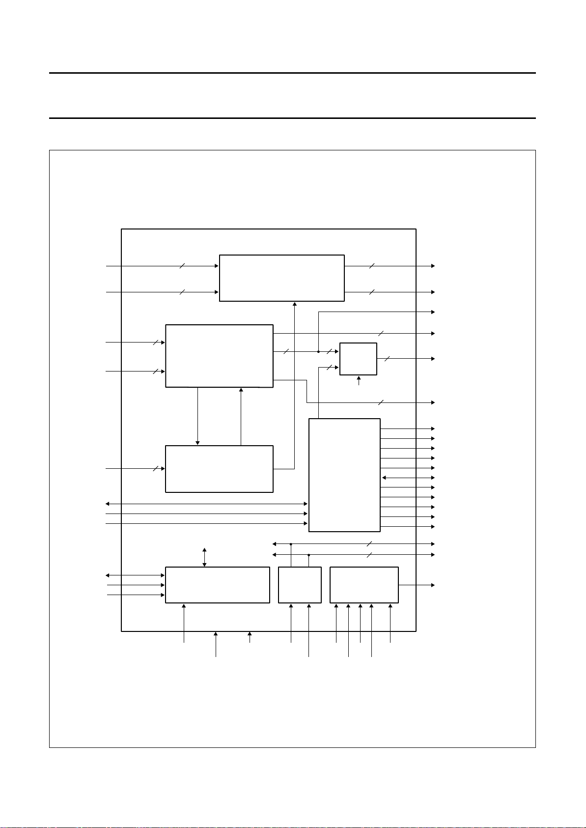
5 BLOCK DIAGRAMS
handbook, full pagewidth
Y_ADC
Y_FM1
U_ADC
V_ADC
U_FM1
V_FM1
17 to 24
1 to 8
15, 16,
13, 14
11, 12,
9, 10
8
8
4
CHROMINANCE
4
PROCESSING
UV_IFA
SAA4996H
LUMINANCE AND
HELPER PROCESSING
4
CS
YL
SAA4996H
60, 59,
57 to 52
8
37 to 44
8
45
61, 62,
63, 64
4
3
1
MUX
3
0
SEL
IVericN
46, 47,
48
3
91, 92,
4
89, 90
Y_MA
Y_TO_FM1
U_TO_FM1_0
U_MA, V_MA
WE_FM2 / U_TO_FM1_1
WE_FM3 / V_TO_FM1_1
RSTW_FM23 / V_TO_FM1_0
U_TO_FM4
V_TO_FM4
U_FM4
V_FM4
VA_FRONT
CLAMP
WE_FRONT
SNERT_DA
SNERT_CL
SNERT_RST
85, 86,
87, 88
81
29
36
82
83
84
4
VERIC_AV_N
CHROMINANCE
MOTION DETECTION
AND IRXR
control
SNERT INTERFACE
25, 49,
67, 73,
96
V
DD1
to V
V
SS1
DD5
26, 50,
66, 74,
CLK_16i
CLK_32i
97
to V
SS5
CLOCK
BUFFER
CLK_16
CLK_32
CONTROL
70332758 72 71 69
TDI
TMS
TCK
TEST
TRSTN
3
3
99
100
94
95
93
79
80
28
76
77
78
98, 75, 35
51, 31, 65
68
30,
32, 34
TEST1,2,3
RE_FM1
WE_FM1
RE_FM4
WE_FM4
RST_FM14
VA_AI
HREF_MA
WE_MA
EVEN_FIELD
FILM
INTPOL
CLK_16B1,2,3
CLK_32B1,2,3
TDO_MA
MHA133
1996 Oct 28 4
Fig.1 Block diagram.
Philips Semiconductors Preliminary specification
Motion Adaptive Colour Plus And Control
IC (MACPACIC) for PALplus
RST_FM14
RE_FM4
WE_FM1
H / V
VA_AI_DIFF
LOGIC
VA_RES
WE_FM4
IVericN
Mpip
CLK_16I
CLK_32I
WE_FM3
WE_FM2
16/32 MHz
H_RE / WE
PC2
PIXEL
PRE
RSTW_FM23
CONVERTER
6
PIXEL
DECODER
11
10 BIT
CLK
COUNTER 2
2 CLK_16
IVericN
LD = 2
line2_every_field
EVEN_FIELD
2
HlpM0,1
RE_FM1
V_RE / WE
LINE
DECODER
IVericN
6
HREF_MA
DELAY
CLAMP
WE_MA
FILM
2
HlpM0,1
VERIC
CONTROL
FilmOn
INTPOL
DECODER
Mpip
EVEN_FIELD
22Valid
SAA4996H
TDO_MA
TEST AND BST
MHA137
TEST3
TEST2
TRSTN TDI TMS TCK TEST1
VA_AI_DIFF
handbook, full pagewidth
VA_AI
Mpip
1
1
Mpip
0
VA_RES
VA_FR_DEL
0
CLK_16I
LC_ACQ
9
ACQ
LINE
PRE
DELAY
VA_FRONT
FIELD LENGTH
InvO/E
IVericN
9 BIT
COUNTER
CLK_16I
3
VaDel0-2
EVEN_FIELD
VA_AI
FIELD
DETECTION,
MEASUREMENT,
VA_RES
CLK_16I
CLP_DIFF
VA_FR_DEL
LD = 1
EN
CLP_DIFF
CLK_16I
PC2_PRE
(1/2 LINE)
VA_AI DELAY
PC1
LC_DSP
DSP
PRE
MUX2
0
1
1
VA_AI_DIFF
LINE
SEL
MUX1
CLK_16I
CLK_16I
CLK_16I
9
9 BIT
COUNTER
EN
Mpip
SEL
0
LD = 1
IVericN
PRE
CLK_16I
WE_MA
WE_MA
GENERATION
PC1
10
PIXEL
10 BIT
COUNTER 1
CLK_32I
CLOCK
BUFFER
WeShift16_0,1
WeStrtH,V
WeStpH,V
36
LD = 2
CLK
CLK_16I
line2_every_field
EnIRXR
MpipFilmOn InvO/EMacpOn MotVis0,1
2 32
HlpM0,1
Preset VaDel0-2
3
7
7
SNERT INTERFACE
5
40
64
Control 6:
Interlace,
EnPreEvFld,
PreEvFld
Control 5:
BOH0-2,
VAA0,1,
SEL_SD_YL0,1,
Control 4:
SelSdYl0,1,
NmYl0,1,
Rha/Rhb0-2
Control 3:
22/23/623Valid,
IMacpacicN,
IVericN
IrxrThr1-4,
FixHlpMain
HlpRedThr1-5,
MacpYhThr1-3
NAIRXR
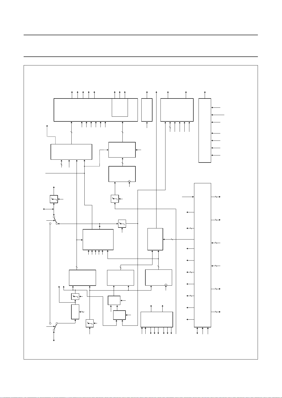
Fig.2 Block diagram of the control part.
VA_FRONT
1996 Oct 28 5
CLAMP
CLK_32
CLK_16
CLK_16B1
CLK_16B2
CLK_16B3
CLK_32B1
CLK_32B2
CLK_32B3
WE_FRONT
SNERT_CL
SNERT_DA
SNERT_RST
Philips Semiconductors Preliminary specification
Motion Adaptive Colour Plus And Control
IC (MACPACIC) for PALplus
Control 1
Control 2
Control 5
handbook, full pagewidth
Control 4
8
8
OUTPUT
REGISTER
2 ACQ DATA
8
FastTest_Del
SNERT_RST
adr_H65/H66
(bit D3)
FastTest
FAST TEST DELAY
8
8
DATA
INPUT
REGISTER
2 SYNCHRON
Control 2/2
Control 1/2
8
8
2 ACQ DATA
Control 1/1
Control 2/1
8
8
Line2_odd_every_field
INPUT
REGISTER
WeStrtH,
WeStpH
2 × 8
4 ACQ DATA
WeStrtH*,
WeStpH*
2 × 8
WeStrtV,
2 × 9
INPUT
REGISTER
2 × 9
WeStpV
WeStrtV*,
HlpRedThr1,2,3,4,5,
MacpYhThr1,2,3,
IrxrThr1,2,3,4,
FixHlpMain,
Control 5
14 × 8
1 SYNCHRON
SNERT_RST
WeStpV*
SAA4996H
Control 6
8
DATA
INPUT
REGISTER
Control 6/1
8
MHA138
Line2_every_field
DATA_OUT
to
21
adr_en_50h
ADDRESS
DECODER
ALE
DLE
REGISTER
SERIAL DATA I/O
DATA AND ADDRESS
SNERT_DA
21 ACTUAL
adr_en_68h
GENERATION
LATCH ENABLE
SNERT_CL
SNERT_RST
DATA
INPUT
REGISTER
DATA_IN
8
4 BIT COUNTER
SEND / RECEIVE
SNERT_RST
CONTROLLING
Interlace
Line2_odd_every_field
LINE 2
GENERATION
ENABLE SIGNAL
ODD / EVERY FIELD
EVEN_FIELD
Line2_every_field
Fig.3 Block diagram of the SNERT interface.
1996 Oct 28 6

Philips Semiconductors Preliminary specification
Motion Adaptive Colour Plus And Control
SAA4996H
IC (MACPACIC) for PALplus
6 PINNING
SYMBOL PIN DESCRIPTION
Y_FM1_7 1 CVBS/helper/luminance input data bit 7 from FM1
Y_FM1_6 2 CVBS/helper/luminance input data bit 6 from FM1
Y_FM1_5 3 CVBS/helper/luminance input data bit 5 from FM1
Y_FM1_4 4 CVBS/helper/luminance input data bit 4 from FM1
Y_FM1_3 5 CVBS/helper/luminance input data bit 3 from FM1
Y_FM1_2 6 CVBS/helper/luminance input data bit 2 from FM1
Y_FM1_1 7 CVBS/helper/luminance input data bit 1 from FM1
Y_FM1_0 8 CVBS/helper/luminance input data bit 0 from FM1
V_FM1_0 9 chrominance input data bit 0 from FM1
V_FM1_1 10 chrominance input data bit 1 from FM1
U_FM1_0 11 chrominance input data bit 0 from FM1
U_FM1_1 12 chrominance input data bit 1 from FM1
V_ADC_0 13 chrominance input data bit 0 from ADC
V_ADC_1 14 chrominance input data bit 1 from ADC
U_ADC_0 15 chrominance input data bit 0 from ADC
U_ADC_1 16 chrominance input data bit 1 from ADC
Y_ADC_0 17 CVBS/helper/luminance data input bit 0 from ADC
Y_ADC_1 18 CVBS/helper/luminance data input bit 1 from ADC
Y_ADC_2 19 CVBS/helper/luminance data input bit 2 from ADC
Y_ADC_3 20 CVBS/helper/luminance data input bit 3 from ADC
Y_ADC_4 21 CVBS/helper/luminance data input bit 4 from ADC
Y_ADC_5 22 CVBS/helper/luminance data input bit 5 from ADC
Y_ADC_6 23 CVBS/helper/luminance data input bit 6 from ADC
Y_ADC_7 24 CVBS/helper/luminance data input bit 7 from ADC
V
DD1
V
SS1
CLK_16 27 16 MHz line-locked system clock input pulse
WE_MA 28 write enable output signal; defines active video data
CLAMP 29 horizontal reference input pulse
TEST1 30 test pin 1; must be LOW during normal operation
CLK_32B2 31 32 MHz line-locked clock output pulse
TEST2 32 test pin 2; must be LOW during normal operation
CLK_32 33 32 MHz line-locked system clock input pulse
TEST3 34 test pin 3; must be LOW during normal operation
CLK_16B3 35 16 MHz line-locked clock output pulse
WE_FRONT
Y_TO_FM1_0 37 CVBS/helper/luminance output data bit 0 to FM1; stand-alone MACPACIC
Y_TO_FM1_1 38 CVBS/helper/luminance output data bit 1 to FM1; stand-alone MACPACIC
Y_TO_FM1_2 39 CVBS/helper/luminance output data bit 2 to FM1; stand-alone MACPACIC
25 positive supply voltage 1
26 negative supply voltage 1
36
write enable input signal used as horizontal reference in the event of active
data
1996 Oct 28 7

Philips Semiconductors Preliminary specification
Motion Adaptive Colour Plus And Control
SAA4996H
IC (MACPACIC) for PALplus
SYMBOL PIN DESCRIPTION
Y_TO_FM1_3 40 CVBS/helper/luminance output data bit 3 to FM1; stand-alone MACPACIC
Y_TO_FM1_4 41 CVBS/helper/luminance output data bit 4 to FM1; stand-alone MACPACIC
Y_TO_FM1_5 42 CVBS/helper/luminance output data bit 5 to FM1; stand-alone MACPACIC
Y_TO_FM1_6 43 CVBS/helper/luminance output data bit 6 to FM1; stand-alone MACPACIC
Y_TO_FM1_7 44 CVBS/helper/luminance output data bit 7 to FM1; stand-alone MACPACIC
U_TO_FM1_0 45 chrominance output data to FM1; stand-alone MACPACIC
WE_FM2/U_TO_FM1_1 46 for full PALplus module; write enable for FM2 for stand-alone MACPACIC;
chrominance output to FM1
RSTW_FM23/V_TO_FM1_0 47 for full PALplus module; reset write for FM2/FM3 for stand-alone
MACPACIC; chrominance output to FM1
WE_FM3/V_TO_FM1_1 48 for full PALplus module; write enable for FM3 for stand-alone MACPACIC;
chrominance output to FM1
V
DD2
V
SS2
CLK_32B1 51 32 MHz line-locked clock output pulse
Y_MA_0 52 luminance output data bit 0 from MACPACIC
Y_MA_1 53 luminance output data bit 1 from MACPACIC
Y_MA_2 54 luminance output data bit 2 from MACPACIC
Y_MA_3 55 luminance output data bit 3 from MACPACIC
Y_MA_4 56 luminance output data bit 4 from MACPACIC
Y_MA_5 57 luminance output data bit 5 from MACPACIC
VERIC_AV_N 58 input configuration signal VERIC available (VERIC_AV_N = 0)
Y_MA_6 59 luminance output data bit 6 from MACPACIC
Y_MA_7 60 luminance output data bit 7 from MACPACIC
U_MA_0 61 chrominance output data bit 0 from MACPACIC
U_MA_1 62 chrominance output data bit 1 from MACPACIC
V_MA_0 63 chrominance output data bit 0 from MACPACIC
V_MA_1 64 chrominance output data bit 1 from MACPACIC
CLK_32B3 65 32 MHz line-locked clock output pulse
V
SS3
V
DD3
TDO_MA 68 boundary scan test: data output signal
TRSTN 69 boundary scan test: reset input signal
TDI 70 boundary scan test: data input signal
TMS 71 boundary scan test: multiplexer set input
TCK 72 boundary scan test: clock input signal
V
DD4
V
SS4
CLK_16B2 75 16 MHz line-locked clock output pulse
EVEN_FIELD 76 even field =0 = odd input field; even field =1 = even input field
49 positive supply voltage 2
50 negative supply voltage 2
66 negative supply voltage 3
67 positive supply voltage 3
73 positive supply voltage 4
74 negative supply voltage 4
1996 Oct 28 8

Philips Semiconductors Preliminary specification
Motion Adaptive Colour Plus And Control
SAA4996H
IC (MACPACIC) for PALplus
SYMBOL PIN DESCRIPTION
FILM 77 control output signal to select film or camera mode in VERIC;
FILM = 0: camera mode; FILM = 1: film mode; FILM = 1 and INTPOL = 0;
bypass mode for MultiPIP
INTPOL 78 INTPOL = 0 = vertical interpolation in the VERIC not active;
INTPOL = 1 = vertical interpolation in the VERIC active
VA_AI 79 vertical reference output pulse or vertical reference input pulse in MultiPIP
mode
HREF_MA 80 horizontal reference output pulse
VA_FRONT 81 vertical reference input pulse or vertical reference output pulse in MultiPIP
mode
SNERT_DA 82 Synchronous No parity Eight bit Reception and Transmission (SNERT)-bus
data
SNERT_CL 83 SNERT-bus clock
SNERT_RST 84 SNERT-bus reset
U_FM4_0 85 chrominance input data bit 0 from FM4
U_FM4_1 86 chrominance input data bit 1 from FM4
V_FM4_0 87 chrominance input data bit 0 from FM4
V_FM4_1 88 chrominance input data bit 1 from FM4
V_TO_FM4_1 89 chrominance output data bit 1 to FM4
V_TO_FM4_0 90 chrominance output data bit 0 to FM4
U_TO_FM4_1 91 chrominance output data bit 1 to FM4
U_TO_FM4_0 92 chrominance output data bit 0 to FM4
RST_FM14 93 reset read/write FM1 and FM4 output
RE_FM4 94 read enable FM4 output
WE_FM4 95 write enable FM4 output
V
DD5
V
SS5
CLK_16B1 98 16 MHz line-locked clock output pulse
RE_FM1 99 read enable FM1 output
WE_FM1 100 write enable FM1 output
96 positive supply voltage 5
97 negative supply voltage 5
1996 Oct 28 9
Philips Semiconductors Preliminary specification
Motion Adaptive Colour Plus And Control
IC (MACPACIC) for PALplus
handbook, full pagewidth
Y_FM1_7
Y_FM1_6
Y_FM1_5
Y_FM1_4
Y_FM1_3
Y_FM1_2
Y_FM1_1
Y_FM1_0
V_FM1_0
V_FM1_1
U_FM1_0
U_FM1_1
V_ADC_0
V_ADC_1
U_ADC_0
U_ADC_1
Y_ADC_0
Y_ADC_1
Y_ADC_2
Y_ADC_3
Y_ADC_4
Y_ADC_5
Y_ADC_6
Y_ADC_7
V
DD1
V
SS1
CLK_16
WE_MA
CLAMP
TEST1
SS5VDD5
WE_FM4
V
CLK_16B1
RE_FM1
WE_FM1
99989796959493929190898887868584838281
100
1
2
3
4
5
6
7
8
9
10
11
12
13
14
15
16
17
18
19
20
21
22
23
24
25
26
27
28
29
RST_FM14
RE_FM4
U_TO_FM4_0
SAA4996H
V_TO_FM4_1
V_TO_FM4_0
U_TO_FM4_1
V_FM4_0
V_FM4_1
U_FM4_0
U_FM4_1
SNERT_DA
SNERT_CL
SNERT_RST
VA_FRONT
80
HREF_MA
79
VA_AI
78
INTPOL
77
FILM
76
EVEN_FIELD
75
CLK_16B2
74
V
73
V
72
TCK
71
TMS
70
TDI
69
TRSTN
68
TDO_MA
67
V
66
V
65
CLK_32B3
64
V_MA_1
63
V_MA_0
U_MA_1
62
61
U_MA_0
60
Y_MA_7
59
Y_MA_6
VERIC_AV_N
58
57
Y_MA_5
56
Y_MA_4
55
Y_MA_3
Y_MA_2
54
53
Y_MA_1
52
Y_MA_0
5130
CLK_32B1
SAA4996H
SS4
DD4
DD3
SS3
1996 Oct 28 10
31323334353637383940414243444546474849
TEST2
TEST3
CLK_32
CLK_32B2
CLK_16B3
WE_FRONT
Y_TO_FM1_0
Y_TO_FM1_1
Y_TO_FM1_2
Y_TO_FM1_3
Y_TO_FM1_4
Y_TO_FM1_5
Y_TO_FM1_6
Y_TO_FM1_7
U_TO_FM1_0
WE_FM2/U_TO_FM1_1
RSTW_FM23/V_TO_FM1_0
WE_FM3/V_TO_FM1_1
Fig.4 Pin configuration.
V
DD2
50
V
MHA134
SS2

Philips Semiconductors Preliminary specification
Motion Adaptive Colour Plus And Control
IC (MACPACIC) for PALplus
7 FUNCTIONAL DESCRIPTION
7.1 Introduction
The MACPACIC is designed to be used in the PALplus
decoder module of a PALplus colour TV receiver. The full
PALplus decoder module consists of two special
integrated circuits and four field memories, as illustrated in
Fig.5.
The special ICs are as follows;
• Motion Adaptive Colour Plus And Control IC
(MACPACIC) for PALplus (SAA4996H)
• Vertical Reconstruction IC (VERIC) (SAA4997H).
Besides the full PALplus module, a configuration for
stand-alone Motion Adaptive Colour Plus processing
(MACP) is also possible (see Fig.6). In this event only
MACPACIC with FM1 and FM4 are necessary.
This configuration enables the MACP processing in
non-PALplus receivers to be performed.
The PALplus module is designed to operate in conjunction
with a 100 Hz feature box. All special requirements such
as the delay of the PALplus module, bypass modes and
generation of the necessary control and clock signals will
be fulfilled.
7.1.1 D
The MACPACIC includes the decompanding functions for
the helper lines and the motion adaptive
luminance/chrominance separation in accordance with the
PALplus system description REV. 3.0 with some
modifications;
• The system operates at a clock frequency of 16 MHz
• The Y:U:V format is 4:1:1 instead of 4:2:2
• The filter DEC_MD_UV_LPF is not implemented
• If noisy helper signals are received, the helper
bandwidth and/or amplitude can be reduced
• Automatic gain control of the helper signal with respect
to the luminance signal.
The input signals are the BB(helper)/CVBS and
chrominance signals which are derived from the
analog-to-digital converter (ADC).
ATA PROCESSING
SAA4996H
7.1.2 C
Memory control, PALplus system controlling and clock
generation (from the incoming 16 MHz and 32 MHz
line-locked clocks) are implemented in the MACPACIC.
All clocks and control signals necessary for the PALplus
module (excluding read control of FM2/FM3) are
generated in the controller part. Inputs are reference
signals, clocks and control signals delivered by the
colour/helper decoder IC (TDA9144), and the 100 Hz
memory controller, i.e. ECO4 (SAA4952) or ECOBENDIC
(SAA4970). The MACPACIC also receives control
information via a three-wire serial interface (SNERT-bus)
from the microprocessor in the 100 Hz feature box.
7.2 General requirements
The PALplus IC set is designed to operate in conjunction
with the PHILIPS 100 Hz feature box. All requirements
with respect to this combination are fulfilled.
The special requirements are as follows;
• The signal processing is adapted to the analog
preprocessing in the TDA9144 for luminance, helper
and chrominance signals
• Clock rate and clock generation
• Some special control signals are generated in the
PALplus module
• The field length must be measured and used to set the
delay of the full PALplus module to 1.5 fields
• A SNERT interface is used to transfer control data to
and from the PALplus module
• MultiPIP with the help of a PIP module is possible
• Results of noise measurements influence the helper
processing
• Automatic gain and offset control is implemented
• Reference signals in line 22 are used for inverse set-up
operation
• Noise measurement implemented
• Boundary scan test implemented
• Preset of internal recursive parts for testing.
ONTROL
At its outputs the MACPACIC delivers separate luminance
and chrominance signals, each one free from
cross-artefacts as main signal, as well as decompanded
and filtered helper signals. For standard input signals and,
in the event of MultiPIP mode with the help of a
PIP module, the MACPACIC can be switched to different
bypass modes.
1996 Oct 28 11

Philips Semiconductors Preliminary specification
Motion Adaptive Colour Plus And Control
IC (MACPACIC) for PALplus
7.3 Hardware configurations and delays
Two general hardware configurations are possible.
7.3.1 F
The delay from input to output is 1.5 fields rounded to
complete lines, also in the bypass mode. Therefore, the
number of input lines of the odd and even fields must be
measured. The result of this measurement is then used to
generate the required delay.
In the MultiPIP mode the delay of the full PALplus module
is one line.
7.3.2 S
In this situation only the MACPACIC with FM1 and FM4
are necessary. No helper lines are processed and no
vertical reconstruction with the VERIC is applied.
The delay from input to output is one field, one line and
some clocks of processing delay, this also applies in the
bypass mode. In the MultiPIP mode the delay is two clocks
(CLK_16).
ULL PALPLUS MODULE (see Fig.5)
TAND-ALONE MACPACIC (see Fig.6)
SAA4996H
7.4 Analog processing in front of the PALplus
module
In front of the MACPACIC an analog colour/helper
decoder (TDA9144) performs the colour and helper
demodulation.
Because of the requirement that a standard ADC with
clamping on 16 should be used for CVBS and helper
analog-to-digital conversion, a black (letter box lines) and
mid grey (helper lines) shift is applied in the colour/helper
decoder. For reshifting without errors in the digital domain
these shift levels are inserted as a reference in line 22.
In the event of stand-alone MACPACIC and PALplus input
signals the helper demodulation must be switched off.
No special actions are taken in the colour/helper decoder
for chrominance processing.
In this document U will refer to −(B − Y) and V will refer to
−(R − Y).
In combination with the full PALplus module with letter box
input signals (16:9), the PAL delay line of the colour/helper
decoder must be switched off. This is because this function
is also implemented in the vertical reconstruction filter of
the VERIC. For all other input signals and for stand-alone
MACPACIC the PAL delay line must be switched on.
1996 Oct 28 12
Philips Semiconductors Preliminary specification
Motion Adaptive Colour Plus And Control
IC (MACPACIC) for PALplus
handbook, full pagewidth
Y_FRONT[0...7]
U_FRONT[0,1]
V_FRONT[0,1]
8
4
FIELD MEMORY
FM1
SWCK SRCK
CLK_16B1
CLK_16
V
DD1-5
V
SS1-5
CLK_16
CLK_32
VA_FRONT
WE_FRONT
CLAMP
SNERT_DA
SNERT_CL
SNERT_RST
TRSTN
TEST1-3
VERIC_AV_N
TDI
TMS
TCK
8
4
5
5
3
(2)
SAA4996H
Y_ADC_0...7
Y_FM1_0...7
U_FM1_0,1
V_FM1_0,1
U_ADC_0,1
V_ADC_0,1
BB-DECOMPANDING
MOTION ADAPTIVE
LUMINANCE /
CHROMINANCE
SEPARATION
MEMORY CONTROL
PALplus CONTROL
CLOCK GENERATION
SYNC GENERATION
SNERT INTERFACE
U_TO_FM4_0,1
V_TO_FM4_0,1
4
FIELD MEMORY
FM4
Y_MA_0...7
U_MA_0,1
V_MA_0,1
U_FM4_0,1
V_FM4_0,1
4
3
3
8
4
8
2
2
CLK_16B1
CLK_16B1, 2, 3
CLK_32B1, 2, 3
8
FIELD MEMORY
4
8
FIELD MEMORY
4
CLK_32B3
Y_TO_FM1_0...7
U_TO_FM1_0
(1)
WE_FM2
U_TO_FM1_1
RSTW_FM23
V_TO_FM1_0
WE_FM3
V_TO_FM1_1
WE_FM1, RE_FM1
RST_FM14
WE_FM4, RE_FM4
VA_AI
WE_MA
HREF_MA
FILM
EVEN_FIELD
INTPOL
TDO_MA
(1)
(1)
CLK_32B1
FM2
FM3
8
4
8
4
V
DD1-4
V
SS1-4
CLK_16B2
CLK_32B3
HREF_MA
VA_AI
FILM
EVEN_FIELD
INTPOL
TRSTN
TDI
TMS
TCK
TEST1-3
NC
8
Y_FM23_0...7
U_FM23_0,1
4
V_FM23_0,1
4
RECONSTRUCTION
4
3
11
SAA4997H
Y_VE_0...7
U_VE_[0,1]
V_VE_[0,1]
INVERSE QMF
FILTER
VERTICAL
CHROMINANCE
SRC
FM2 / FM3
READ CONTROL
MHA136
SAA4996H
8
Y_VE_[0...7]
U_VE_0,1
4
V_VE_0,1
TDO_VE
OE_FM2
OE_FM3
RE_FM2
RE_FM3
RSTR_FM23
(1) In case of stand-alone MACPACIC the output signals are U_TO_FM1_1, V_TO_FM1_0 or V_TO_FM1_1.
Otherwise the output signals are WE_FM2, RSTW_FM23 or WE_FM3.
(2) VERIC available: VERIC_AV_N is connected to V
1996 Oct 28 13
.
SS
Fig.5 PALplus decoder module.
Philips Semiconductors Preliminary specification
Motion Adaptive Colour Plus And Control
IC (MACPACIC) for PALplus
handbook, full pagewidth
Y_FRONT[0...7]
U_FRONT[0,1]
V_FRONT[0,1]
8
FIELD MEMORY
FM1
SWCK SRCK
4
CLK_16
CLK_16B1
V
DD1-5
V
SS1-5
CLK_16
CLK_32
VA_FRONT
WE_FRONT
CLAMP
SNERT_DA
SNERT_CL
SNERT_RST
TRSTN
TEST1-3
VERIC_AV_N
TDI
TMS
TCK
(2)
8
4
5
5
3
Y_ADC_0...7
Y_FM1_0...7
U_FM1_0,1
V_FM1_0,1
U_ADC_0,1
V_ADC_0,1
MOTION ADAPTIVE
CHROMINANCE
MEMORY CONTROL
PALplus CONTROL
CLOCK GENERATION
SYNC GENERATION
SNERT INTERFACE
U_TO_FM4_0,1
V_TO_FM4_0,1
4
Y_TO_FM1_0...7
Y_TO_FM1_0
SAA4996H
LUMINANCE /
SEPARATION
U_FM4_0,1
V_FM4_0,1
SAA4996H
8
Y_MA_0...7 Y_MA_0...7
U_MA_0,1
V_MA_0,1
4
8
4
RSTW_FM23
V_TO_FM1_0
WE_FM2
U_TO_FM1_1
WE_FM3
V_TO_FM1_1
3
CLK_16B1, 2, 3
3
CLK_32B1, 2, 3
2
WE_FM1, RE_FM1
RST_FM14
2
WE_FM4, RE_FM4
VA_AI
WE_MA
HREF_MA
FILM
EVEN_FIELD
INTPOL
TDO_MA
U_MA_0,1
V_MA_0,1
(1)
(1)
(1)
(1) In case of stand-alone MACPACIC the output signals are U_TO_FM1_1, V_TO_FM1_0 or V_TO_FM1_1.
Otherwise the output signals are WE_FM2, RSTW_FM23 or WE_FM23.
(2) VERIC not available: VERIC_AV_N is connected to V
1996 Oct 28 14
FIELD MEMORY
FM4
.
DD
Fig.6 Stand-alone MACPACIC.
CLK_16B1
MHA135

Philips Semiconductors Preliminary specification
Motion Adaptive Colour Plus And Control
IC (MACPACIC) for PALplus
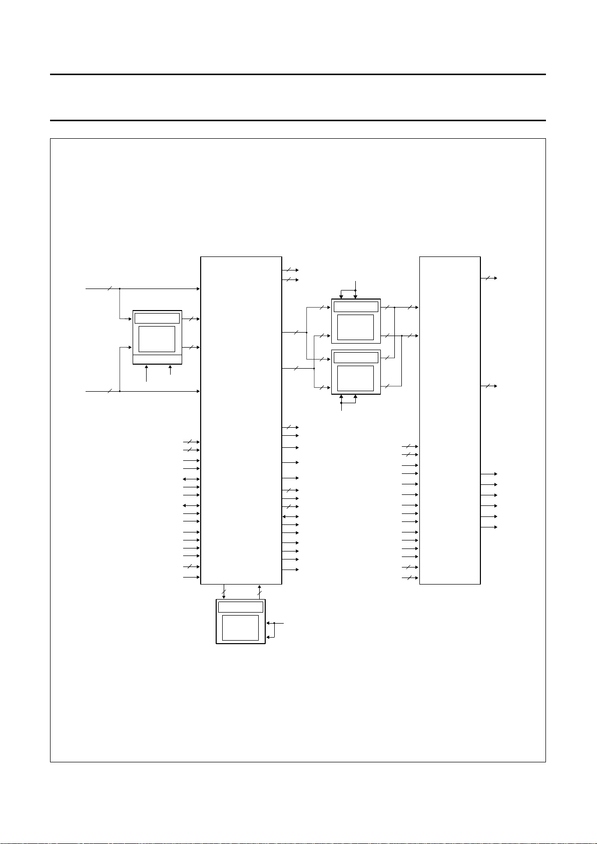
7.5 Block diagram
The functional block diagram of the MACPACIC for
PALplus is illustrated in Fig.1. The device consists of
4 main parts:
• Luminance and helper processing
• Chrominance processing
• Chrominance motion detection
• Control.
The clock rate of the input data is 16 MHz. Internally, the
device operates at a 32 MHz clock frequency. The clock
rate of the output data is either 32 MHz (in combination
with FM2, FM3 and VERIC) or 16 MHz for stand-alone
MACP processing.
The delay of the full PALplus module is 1.5 fields in the
PALplus and bypass mode. A field length measurement is
implemented. For MultiPIP with the help of a PIP module
the delay of the PALplus module is one line.
For stand-alone MACP the delay is one field, one line and
some clocks of processing delay.
For MultiPIP with the help of a PIP module the delay of
MACPACIC is two clocks (CLK_16).
7.6 Luminance and helper processing
7.6.1 I
To use a standard ADC with clamping on 16, a black
set-up for the CVBS signal and a black/mid grey set-up for
the helper signal has to be performed in the colour/helper
decoder. The shift values for black set-up and mid grey
set-up are inserted in line 22.
All values are nominal values.
CVBS:
clamp level: 16
black set-up: 51
white: 191
format: 8-bit, straight binary
Helper:
mid grey set-up: 121
range: (121 − 60) to (121 + 60) = 61 to 181
format: 8-bit, offset binary
NPUT RANGE
SAA4996H
7.7 Luminance processing
The luminance and the helper processing have two input
branches. One input is an 8-bit wide 16 MHz data stream
from the ADC. The other is an 8-bit wide 16 MHz data
stream from the field memory (FM1). The odd field of an
input frame is stored in the field memory FM1. In the even
field of a frame, the even field together with the delayed
odd field is processed by the MACPACIC.
To remove the chrominance part of the incoming
composite video signal, the Motion Adaptive Colour Plus
technique is applied. Colour Plus is a dedicated comb filter
technique, which makes full use of the correlation of two
successive fields.
During processing the data of the odd and even fields are
separated in a high-pass and low-pass part. The high-pass
part consists of the luminance high-pass component and
the modulated chrominance signal. Due to the phase
difference of the colour carrier of 180° from the odd to the
even field, the chrominance signal can be removed by
adding the high-pass signals.
This processing will work successfully in the film mode,
because scanned film material is motionless within the two
fields of one frame. In the camera mode a motion detector
fades down the luminance high-pass component if motion
is detected.
The following vertical low-pass filters perform a vertical
interpolation of the high-pass part by the factor of two.
In the event of bad signal conditions, the residual
cross-luminance signal, caused by clock jitter between two
fields, can be reduced by using this filter as a 2D comb
filter. Therefore different sets of coefficients can be
selected via SNERT.
The luminance high-pass part and the luminance low-pass
part are then added.
The automatic gain control (AGC) and automatic offset
control (AOC) functions use reference lines 23,
623 and 22 to reduce errors in the vertical reconstruction
in the VERIC. This is to reduce the effects of any errors
that might be caused due to variations in the conventional
PAL references in the signal during the transmission chain
with respect to the levels of the luminance letter box and
helper signals.
Y (standard input):
black: 16
peak white: 191
format: 8-bit, straight binary
1996 Oct 28 15

Philips Semiconductors Preliminary specification
Motion Adaptive Colour Plus And Control
IC (MACPACIC) for PALplus
7.7.1 LUMINANCE HELPER PROCESSING
In the event of incoming helper, the switchable low-pass
filter acts as an inverse shaping and bandwidth reduction
filter for the helper lines. If a distorted helper signal is
transmitted, the bandwidth can be reduced from 2.2 MHz
(0 dB) to 1.0 MHz or to 0.5 MHz (−3 dB).
The high-pass part of the luminance processing is not
used for the helper processing.
To stabilize the transmitted helper signal against noise
disturbances, the encoder performs a companding of the
signal. In the decoder the decompanding is performed in
the AGOC block (see Fig.7).
7.8 Output signals
In the event of full PALplus configuration, odd and even
field data are multiplexed to a 32 MHz data stream.
For the stand-alone MACPACIC, the processed even field
data is connected to the field memory FM1 and the odd
field data is switched to the output Y_MA. In the next field
the stored even field data is read out of the field memory
FM1 and then connected to the output of the MACPACIC.
If MultiPIP mode is selected, the luminance input data from
the ADC (Y_ADC) is switched directly to the output Y_MA.
In the bypass mode the luminance data processing is
switched off and multiplexed data is connected to the
MACPACIC output.
The clock frequency of the output data Y_MA is 32 MHz for
the MACPACIC in combination with the VERIC, or 16 MHz
for the stand-alone MACPACIC.
7.9 Measurements
The digital data stream at the input of the PALplus decoder
module contains three reference lines;
• Reference line 22 consists of the black and mid grey
set-up, inserted by the colour/helper decoder
• The second half of line 23 contains the black level
reference and the maximum negative reference for the
PALplus helper lines
• The first half of line 623 contains reference values for
the black level and the peak white level for the main
lines.
The reference lines 23 and 623 are generated by the
PALplus encoder and are used to reduce the effects of any
errors that might be caused due to variations in the
transmission chain with respect to the levels of the
luminance letter box and helper signals.
SAA4996H
The content and the timing of the reference lines are
illustrated in Figs 13, 14 and 15.
7.9.1 L
Due to the fact that a standard ADC with a clamping level
of 16 should be inserted for CVBS and helper
analog-to-digital conversion, a black offset for the letter
box lines and a mid grey offset for the helper lines are
carried out in the colour/helper decoder. These offset
values are inserted as references in line 22 to reshift the
CVBS and helper signals in the digital domain without
errors. Therefore, a measurement of the offsets in line 22
is necessary. The average value of the real offset is
calculated from 64 samples and substacted from the
CVBS and helper signal. The CVBS and helper input
signal are illustrated in Fig.16.
7.9.2 L
The helper and luminance amplitude measurement
consists of averaging 64 samples each of;
Helper zero (MHZ).
Helper maximum (MHM).
Luminance black (MLB).
Luminance white (MLW).
Measured helper amplitude = helper maximum minus
helper zero.
Measured luminance amplitude = luminance white minus
luminance black.
Frame integration is performed with a feed back factor of
(1 − K) =1⁄16. The frame integration part can be preset with
the first measured value. Preset is controlled with the
preset bit transmitted via SNERT.
7.9.3 N
For the helper lines the noise measurement is carried out
in reference line 23 and for the letter box lines in reference
line 623. Both measurements are active in the black
reference levels of line 23 and line 623 respectively.
The processing of the noise measurement for the helper
signal and the letter box signal is performed in the same
way.
First the average value of 64 samples is calculated.
The single actual sample values are subtracted from this
average value and the sum of these absolute differences
are frame integrated. The integration factor is 1 − K=1⁄16.
INE 22 OFFSET REFERENCE MEASUREMENT
INE 23 AND 623 AMPLITUDE REFERENCE
MEASUREMENT
OISE MEASUREMENT IN LINE 23 AND 623
1996 Oct 28 16

Philips Semiconductors Preliminary specification
Motion Adaptive Colour Plus And Control
IC (MACPACIC) for PALplus
The frame integration part can be preset with the first
measured value. Preset is controlled via a bit from the
SNERT interface.
7.10 Automatic gain and offset control
The automatic gain and offset control circuit evaluates the
results of the reference data, which are derived from
reference lines 22, 23 and 623 to eliminate any offset and
gain differences between the letter box lines and the
helper lines. This is caused during transmission of the
video signal.
7.10.1 SNERT
AOC
MacpOn: If line 22 is not detected this bit will be ignored
and the MACP processing (and thus AGC and AOC) is
switched off.
FilmOn: If line 22 is not detected, the VERIC operates in
Camera mode.
CONTROL BITSINFLUENCING THE AGC AND
SAA4996H
The helper amplitude is reduced when the measured noise
exceeds a certain threshold level. These thresholds are
conveyed via the SNERT-bus. The reduction of the helper
amplitude, before decompanding, ensures that more noise
is cancelled by the coring. The adaptive helper gain control
is switched off when the SNERT bits HlpM1 and HlpM0 are
both at logic 1. In this condition the helper gain is defined
by the values FixHlp and FixMain via the SNERT-bus.
If the measured helper or luminance amplitude is below
the threshold level, or when line 22 is not valid, the helper
is switched off.
7.10.3 O
As long as line 22 reference is present, luminance and
helper offset are controlled by line 22. If line 22 is not valid
the offset value is fixed to 16.
For luminance offset control a hysteresis function,
controlled by SNERT, is applied to the measured
luminance offset.
FFSET CONTROL
HlpM1, HlpM0: In adaptive and fixed helper processing
modes (HlpM1 = 1, HlpM0 = X) AGC and AOC are
achieve.
Table 1 Control bits HlpM1 and HlpM0
HlpM1 HlpM0 FUNCTION
0 0 no helper processing
(any aspect ratio, without helper)
0 1 helper set to zero
(up-conversion without helper)
1 0 adaptive helper processing (helper
processing controlled by reference
amplitudes and noise in the helper
channel)
1 1 fixed helper processing (fixed gain
values loaded via SNERT-bus)
7.10.2 GAIN CONTROL
If line 22 reference is present in a frame, the luminance
input signal contains black set-up and reduced amplitude.
The luminance gain then is 1.25. If line 22 is not valid the
luminance gain is 1.0.
7.10.4 H
In the event of noisy helper signals the helper amplitude
and bandwidth can be reduced to avoid disturbances in
the inverse QMF processing in VERIC.
Five thresholds are therefore transmitted via SNERT.
These thresholds are compared with the measured helper
noise value. The results are used to control a state
machine with five states.
The state machine is initialized with the preset bit from
SNERT or when line 22 is valid for the first time.
The output states are used to control the helper amplitude
and bandwidth as shown in Fig.8 and Tables 2 and 3.
7.11 Output range
Luminance lines: straight binary, black = 16, white = 191.
PALplus helper lines: offset binary, 128 ±70.
ELPER AMPLITUDE AND BANDWIDTH CONTROL
The helper gain is controlled by the measured helper
amplitude in line 23 to match the helper amplitude to the
decompanding table. After decompanding the helper
amplitude is controlled by the measured luminance
amplitude in line 623, to obtain the correct
luminance/helper ratio for the QMF filter in the VERIC.
1996 Oct 28 17

Philips Semiconductors Preliminary specification
Motion Adaptive Colour Plus And Control
IC (MACPACIC) for PALplus
Y_MA
Y_TO_FM1
MUX
Y_FM1
Y_ADC
AGOC
SAA4996H
MHA300
results
measurement
AGOC
+
LM
Y_LP (even)
SWITCHABLE
Y_HP (even)
FILTER
LOW-PASS
HIGH-PASS
Y_ADC
VERTICAL
YL
detector)
from motion
(fade controlled
FILTER
MEASUREMENTS
LPF
3 TAB
X
Y_HP
+
LPF
3 TAB
VERTICAL
Y_HP (odd)
FILTER
HIGH-PASS
SWITCHABLE
+
LM
Y_LP (odd)
FILTER
LOW-PASS
Y_FM1
Fig.7 Luminance and helper processing.
1996 Oct 28 18
handbook, full pagewidth

Philips Semiconductors Preliminary specification
Motion Adaptive Colour Plus And Control
IC (MACPACIC) for PALplus
state machine
handbook, halfpage
output
4
3
2
1
0
HlpRedThr1
HlpRedThr2
HlpRedThr3
HlpRedThr4
Fig.8 Helper bandwidth and amplitude reduction.
Measured Helper
Noise (MHN)
HlpRedThr5
SAA4996H
MHA295
Table 2 Measured Helper Noise in Zero (MHNZ)
MHNZ STATE MACHINE (OLD) STATE MACHINE (NEW)
MHNZ < HlpRedThr1 X 4
HlpRedThr1 ≤ MHNZ < HlpRedThr2 4 4
<4 3
HlpRedThr2 ≤ MHNZ < HlpRedThr3 ≥33
<3 2
HlpRedThr3 ≤ MHNZ < HlpRedThr4 ≥22
<2 1
HlpRedThr4 ≤ MHNZ < HlpRedThr5 ≥11
00
HlpRedThr5 ≤ MHNZ X 0
Table 3 State machine output
STATE MACHINE OUTPUT REDUCE HELPER BANDWIDTH (RHB) REDUCE HELPER AMPLITUDE (RHA)
4 0 (2.2 MHz LPF) 2; note 1
3 1 (1.0 MHz LPF) 2
2 1 (1.0 MHz LPF) 1; note 2
1 2 (0.5 MHz LPF) 1
0 2 (0.5 MHz LPF) 0; note 3
Notes
1. No helper amplitude reduction.
2. Helper amplitude reduction via LUT of about 50%.
3. Helper signal zero.
1996 Oct 28 19

Philips Semiconductors Preliminary specification
Motion Adaptive Colour Plus And Control
IC (MACPACIC) for PALplus
7.12 Chrominance
7.12.1 I
The input is a 4:1:1 sequential 4-bit wide UV signal with a
16 MHz clock frequency. Originally the U and V signals
were 8 bits wide with a sampling frequency of 4 MHz each.
The range is 0 ±90 in two’s complement format for
U and V.
7.12.2 C
The Motion Adaptive Colour Plus technique is also applied
in the chrominance processing to remove the luminance
part from the incoming demodulated UV signal.
In the modulated domain the chrominance signal can be
generated by subtracting the odd and even field data due
to the 180° phase difference of the colour subcarrier.
The colour decoder eliminates the phase difference of the
chrominance signals, but now the luminance signals will
obtain the phase difference of 180°.
By adding the odd and even field data, the cross-colour
free chrominance signal (UVifa) is generated.
This processing will work successfully in the film mode,
because scanned film material is motionless within the two
fields of one frame. In the camera mode, where each field
represents an individual picture, a motion detector fades
down the chrominance high-pass component if motion is
detected.
When chrominance motion occurs, the encoder fades
down the high-pass luminance signal. In that event, the
motion detector in the decoder will switch the chrominance
part from intra frame average processing to the incoming
data.
NPUT RANGE
HROMINANCE PROCESSING
SAA4996H
Odd and even field data are multiplexed and connected to
the output of MACPACIC.
The chrominance processing has two input branches (see
Fig.9). One input branch is the direct chrominance input
path from the ADC. The other input branch is the output of
the field memory FM1. The odd field of a frame is stored in
the field memory FM1. In the even field of a frame the
delayed odd field and the incoming even field are
processed with the motion adaptive colour plus algorithm
to the cross-colour free chrominance output data.
By adding the incoming chrominance signals of the odd
and even fields, the intra frame average chrominance
signal (UVifa) is generated.
For the chrominance motion detector this signal is stored
after formatting in the memory FM4 (UV_TO_FM4).
7.12.3 OUTPUT SIGNALS
The output data rate is 32 MHz for MACPACIC in
combination with VERIC and 16 MHz for stand-alone
MACPACIC or in the MultiPIP mode.
In the MultiPIP mode the chrominance data from the ADC
(UV_ADC) is switched directly to the output UV_MA.
In the bypass mode the chrominance data processing is
switched off and the multiplexed odd and even field data
are connected to the MACPACIC output.
7.12.4 O
The range is 0 ±90 in two’s complement format for
U and V.
UTPUT RANGE
handbook, full pagewidth
1996 Oct 28 20
UV_ADC
UV_FM1
(even)
+
(odd)
UVifa
0
1
0
1
MUX
LMMUX
CS
from motion
detector
LM
UV_TO_FM4
to motion detector
Fig.9 Chrominance processing.
MUX
UV_FM1
UV_ADC
MUX
UV_TO_FM1
UV_out
MHA299

Philips Semiconductors Preliminary specification
Motion Adaptive Colour Plus And Control
IC (MACPACIC) for PALplus
7.13 Chrominance motion detection
The PALplus system has two modes of operation.
These are called film mode, which is only used with film
sources, and camera mode which is applied for normal
50 Hz interlaced video sources. The motion detector is
only necessary in the camera mode because, in the
film mode, the two fields of a frame are sampled from the
same picture of the film.
The chrominance motion detector has two input branches
(see Fig.10). One input branch is the intra frame average
of the actual frame, the other input branch is the intra
frame average signal of the previous frame. This signal is
delivered by the field memory FM4.
Subtraction of the two intra frame average signals
generates the chrominance inter frame difference.
PAL averaging eliminates phase errors. This PAL
averaging can be switched off when the PAL delay line in
the colour decoder is active.
A look-up table (LUT) generates the motion signal from the
chrominance signal. A comparator generates a
chrominance control switch signal (CS). A horizontal
interpolation filter interpolates a 16 MHz motion signal.
The motion high-pass luminance control signal M_YL is
provided by another LUT.
7.14 Intelligent residual cross-luminance reduction
(IRXR)
The IRXR block diagram is illustrated in Fig.10.
The MACP algorithm requires good stability of the
sampling clock between both fields, because samples
from both fields will be combined, in order to suppress
cross-colour and cross-luminance. Investigations with
currently used sync/clock circuitry have shown that the
stability of these clocks is not as good as it should be for
perfect performance of the MACP algorithm.
When a MACP signal is received the colour subcarrier trap
in the TDA9144 is bypassed and the input signal of the
SAA4996H still contains the modulated colour component.
The MACP technique always processes corresponding
lines of two successive fields (having an offset of
312 lines). These lines will have the same high-frequency
luminance information (YH) and inverted colour
information due to the phase/line relationship in PAL.
With an ideal sampling grid, the two inverted colour signals
will be cancelled completely by addition so that no
cross-luminance (XL) remains in the resulting picture.
SAA4996H
When the sampling grid is not optimum (e.g. shifted a little
in one field with respect to the other field), the cancellation
of both modulated colour signals will not be complete and
some residual XL will remain. The amount of residual XL
is proportional to the amplitude of the modulated colour
signal and to the following formula;
π f_sc× timing_error×()sin
The timing error is determined by the type of circuitry used
for the sync/clock generation and by the amount of
noise/disturbance in the input signal (more
noise/disturbance generally leads to larger timing errors).
The intelligent residual cross-luminance reduction (IRXR)
tries to cancel this residual cross-luminance (XL), by
reducing the amount of YH depending of the amplitude of
the modulated colour signal.
The saturation indication signal (SD) is generated by the
intra frame average signal of the actual frame with the help
of a look-up table (LUT). A horizontal interpolation filter
interpolates a 16 MHz saturation detection signal SD.
Another LUT transforms the SD signal into the signal
SD_YL, which determines the amount of YH to be
reduced. Different characteristics curves of the LUT can
be selected either via SNERT (SEL_SD_YL) or
automatically depending on the measured noise value
(SelSdYl), see Fig.11 and Table 4.
The IRXR function can be disabled or enabled via SNERT
by the EN_IRXR bit.
The output signal YL is generated from the three YH
reduction signals SD_YL, M_YL and NM_YL.
This combination is performed with a minimum detection
circuit. The amount of YH that is allowed is the lowest of
the three input signals. Whenever one input signal
indicates a reason to reduce the YH, this should be
performed independently of the other input signals.
In the event of film mode the signals NM_YL (Fig.12 and
Table 5) and M_YL are over-written with the value 4.
Motion detector processing is not active for these signals
in the film mode. Such film overriding is not allowed for the
SD_YL signal, because the residual XL can occur in the
film mode as well as in the camera mode.
1996 Oct 28 21

Philips Semiconductors Preliminary specification
Motion Adaptive Colour Plus And Control
IC (MACPACIC) for PALplus
YL
MIN
CS
0
M_YL
M_YL
MUX
M
LUT
1
FilmOn
4
MUX
0
NM_YL
1
4
FilmOn
0
4
MUX
1
SD_YL
SD_YL
SD'
SD'
LUT
MHA298
EN_IRXR
MUX
0
SAA4996H
1
NAIRXR
M
CS
LUT
M
SIGNAL M
THE MOTION
MOTION DETECTOR
LUT TO GENERATE
MUX
0
1
PAL
AVERAGING
−
FILTER
INTERPOLATION
decoder active
PAL averaging in colour
INTERPOLATION
SD
IRXR
LUT TO GENERATE
0
PAL
AVERAGING
FILTER
SIGNAL SD
THE SATURATION
MUX
1
SelSdYl
SEL_SD_YL (from SNERT)
decoder active
PAL averaging in colour
handbook, full pagewidth
Fig.10 Motion detector and intelligent residual cross-luminance reduction (IRXR).
1996 Oct 28 22
UVifa
UV_FM4

Philips Semiconductors Preliminary specification
Motion Adaptive Colour Plus And Control
IC (MACPACIC) for PALplus
state machine
handbook, halfpage
output
3
2
1
0
SatYhThr1
SatYhThr2
SatYhThr3
Measured Luminance
Noise in Black (MLNB)
SatYhThr4
MHA296
state machine
handbook, halfpage
output
2
1
0
MacpYhThr1
MacpYhThr2
SAA4996H
Measured Helper
Noise Zero (MHNZ)
MacpYhThr3
MHA297
Fig.11 Generation of the signal SelSdYl.
Fig.12 Generation of the signal NM_YL.
Table 4 Measured luminance noise in black (MLNB)
MLNB STATE MACHINE (OLD) STATE MACHINE (NEW)
MLNB < SatYhThr1 X 3
SatYhThr1 ≤ MLNB < SatYhThr2 3 3
<3 2
SatYhThr2 ≤ MLNB < SatYhThr3 ≥22
<2 1
SatYhThr3 ≤ MLNB < SatYhThr4 ≥11
00
SatYhThr3 ≤ MLNB X 0
Table 5 Generation of the signal NM_YL
MHNZ STATE MACHINE (OLD) STATE MACHINE (NEW) NM_YL
MHNZ < MacpYhThr1 X 2 4
MacpYhThr1 ≤ MHNZ < MacpYhThr2 2 2 4
<2 1 2
MacpYhThr2 ≤ MHNZ < MacpYhThr3 ≥112
<1 0 0
MacpYhThr3 < MHNZ X 0 0
1996 Oct 28 23

Philips Semiconductors Preliminary specification
Motion Adaptive Colour Plus And Control
IC (MACPACIC) for PALplus
handbook, full pagewidth
255
line time
reference point = half amplitude
191
121
51
16
of the falling synchronisation slope
22 µs
31 µs
11 µs
clamp level
0
0 5 10 15 20 25 30 35 40 45 50 55 60 65
black set-up
mid grey set-up
SAA4996H
MHA148
Fig.13 Digital representation of the reference signal in line 22 at the input of the PALplus decoder module.
handbook, full pagewidth
255
191
51
16
line time
reference point = half amplitude
of the falling synchronisation slope
10.5 µs
clamp level
0
0 5 10 15 20 25 30 35 40 45 50 55 60 65
wide screen signalling bits
41 µs
51 µs
black level
reference
121
maximum negative
reference
10.83 µs
61
MHA149
Fig.14 Digital representation of the reference signal in line 23 at the input of the PALplus decoder module.
1996 Oct 28 24

Philips Semiconductors Preliminary specification
Motion Adaptive Colour Plus And Control
IC (MACPACIC) for PALplus
handbook, full pagewidth
255
line time
reference point = half amplitude
191
of the falling synchronisation slope
30 µs
20 µs
51
16
0
10.5 µs
clamp level
0 5 10 15 20 25 30 35 40 45 50 55 60 65
black level
reference
white level reference
SAA4996H
MHA150
Note: There is no burst in line 623.
Fig.15 Digital representation of the reference signal in line 623 at the input of the PALplus decoder module.
handbook, full pagewidth
255
51
16
white
181
mid grey set-up
black set-up
clamp level
0
CVBS (EBU colour bar with 100% saturation and base band helper with mid grey set-up
75% amplitude) with black set-up
121
61
191
MHA151
1996 Oct 28 25
Fig.16 PALplus CVBS and helper input signal.

Philips Semiconductors Preliminary specification
Motion Adaptive Colour Plus And Control
IC (MACPACIC) for PALplus
handbook, full pagewidth
(clamp level)
WHITE
BLACK
255
191
16
0
SAA4996H
MHA154
handbook, full pagewidth
WHITE
BLACK
Fig.17 Non PALplus Y input signal.
255
191
16
0
MHA155
1996 Oct 28 26
Fig.18 Y output signal.

Philips Semiconductors Preliminary specification
Motion Adaptive Colour Plus And Control
IC (MACPACIC) for PALplus
handbook, full pagewidth
255
198
128
58
16
0
SAA4996H
MHA152
handbook, full pagewidth
Fig.19 Helper output signal.
typical digital values
127
90
60
30
0
–30
–60
–90
52 µs
–128
EBU Colour Bar
12 µs
MHA153
1996 Oct 28 27
Fig.20 −(B − Y) input and output signal.

Philips Semiconductors Preliminary specification
Motion Adaptive Colour Plus And Control
IC (MACPACIC) for PALplus
handbook, full pagewidth
typical digital values
+127
+90
+76
+14
0
−14
−76
−90
52 µs
−128
EBU Colour Bar
SAA4996H
12 µs
MHA294
CLK_16
handbook, full pagewidth
WE_FRONT
Y_ADC_0...7
U_ADC_1
U_ADC_0
V_ADC_1
V_ADC_0
Fig.21 −(R − Y) input and output signal.
XX Y0 Y1 Y2 Y3 Y4 Y5 Y838 Y839 XXXX
XX U70 U50 U30 U010 U74 U54 U3836 U1836 XXXX
XX U60 U40 U20 U00 U64 U44 U2836 U0836 XXXX
XX V70 V50 V30 V10 V74 V54 V3836 V1836 XXXX
XX V60 V40 V20 V00 V64 V44 V2836 V0836 XXXX
MHA163
1996 Oct 28 28
Fig.22 Horizontal data input timing.

Philips Semiconductors Preliminary specification
Motion Adaptive Colour Plus And Control
IC (MACPACIC) for PALplus
handbook, full pagewidth
CLK_16
CLK_32
Y_MA_0..7
U_MA_1
U_MA_0
V_MA_1
V_MA_0
XX XX Y0A Y0B Y1A Y1B Y2A Y2B Y3A Y3B Y4A Y4B
XXXX
XXXX
XXXX
XX XX V70A V50A V30A V10A
XXXX
XXXX
U60A
bit
word
field
SAA4996H
U60B U40B U20B U00B U64A U44AXX XX U70A U50A U30A U10A
U70B U50B U30B U10B U74A U54AXX XX U60A U40A U20A U00A
V60B V40B V20B V00B V64A V44A
V70B V50B V30B V10B V74A V54AXX XX V60A V40A V20A V00A
MHA156
CLK_16
handbook, full pagewidth
Y_MA_0...7
U_MA_1
U_MA_0
V_MA_1
V_MA_0
Fig.23 Horizontal output signals, full PALplus module.
XX Y0 Y1 Y2 Y3 Y4 Y5 Y838 Y839 XX
XX U70 U50 U30 U010 U74 U54 U3836 U1836 XX
XX U60 U40 U20 U00 U64 U44 U2836 U0836 XX
XX V70 V50 V30 V10 V74 V54 V3836 V1836 XX
XX V60 V40 V20 V00 V64 V44 V2836 V0836 XX
MHA157
1996 Oct 28 29
Fig.24 Horizontal output signals, stand-alone MACPACIC.

Philips Semiconductors Preliminary specification
Motion Adaptive Colour Plus And Control
IC (MACPACIC) for PALplus
CLK_16
handbook, full pagewidth
Y_FM1_0...7
U_FM1_1
U_FM1_0
V_FM1_1
V_FM1_0
XX Y0 Y1 Y2 Y3 Y4 Y5 Y838 Y839 XX
XX U70 U50 U30 U010 U74 U54 U3836 U1836 XX
XX U60 U40 U20 U00 U64 U44 U2836 U0836 XX
XX V70 V50 V30 V10 V74 V54 V3836 V1836 XX
XX V60 V40 V20 V00 V64 V44 V2836 V0836 XX
SAA4996H
MHA160
CLK_16
handbook, full pagewidth
Y_TO_FM1_0...7
U_TO_FM1_1
U_TO_FM1_0
V_TO_FM1_1
V_TO_FM1_0
Fig.25 Horizontal timing, data from FM1.
Y838 Y839 XXY0 Y1 Y2 Y3XX XX XX
U70 U50 U30 U010XX XX XX U3836 U1836 XX
U60 U40 U20 U00XX XX XX U2836 U0836 XX
V70 V50 V30 V10XX XX XX V3836 V1836 XX
V60 V40 V20 V00XX XX XX V2836 V0836 XX
MHA161
1996 Oct 28 30
Fig.26 Horizontal timing, data to FM1 for stand-alone MACPACIC.

Philips Semiconductors Preliminary specification
Motion Adaptive Colour Plus And Control
IC (MACPACIC) for PALplus
CLK_16
handbook, full pagewidth
U_FM4_1
U_FM4_0
V_FM4_1
V_FM4_0
U40
SAA4996H
U3836 U1836 XXU70 U50 U30 U010XX XX XX
U20 U00XX XX XX
U2836 U0836 XXU60
V3836 V1836 XXV70 V50 V30 V10XX XX XX
V2836 V0836 XXV60 V40 V20 V00XX XX XX
MHA158
CLK_16
handbook, full pagewidth
U_TO_FM4_1
U_TO_FM4_0
V_TO_FM4_1
V_TO_FM4_0
Fig.27 Horizontal timing, input signals from FM4.
U3836 U1836 XXU70 U50 U30 U010XX XX XX
U2836 U0836 XXU60 U40 U20 U00XX XX XX
V3836
V1836 XXV70 V50 V30 V10XX XX XX
V0836V2836 XXV60 V40 V20 V00XX XX XX
MHA159
1996 Oct 28 31
Fig.28 Horizontal timing, output signals to FM4.

Philips Semiconductors Preliminary specification
Motion Adaptive Colour Plus And Control
IC (MACPACIC) for PALplus
handbook, full pagewidth
line number
21
22
23
24
59
60
274
275
310
311
black and mid grey set-up reference line
wide screen signalling bits
FIELD A
helper (36 lines)
('black band')
letter box (215 lines)
helper (36 lines)
('black band')
SAA4996H
reference signals
335
336
371
372
586
587
622
623
624
FIELD B
helper (36 lines)
('black band')
letter box (215 lines)
helper (36 lines)
('black band')
reference signals
MHA147
Fig.29 PALplus frame.
1996 Oct 28 32

Philips Semiconductors Preliminary specification
Motion Adaptive Colour Plus And Control
IC (MACPACIC) for PALplus
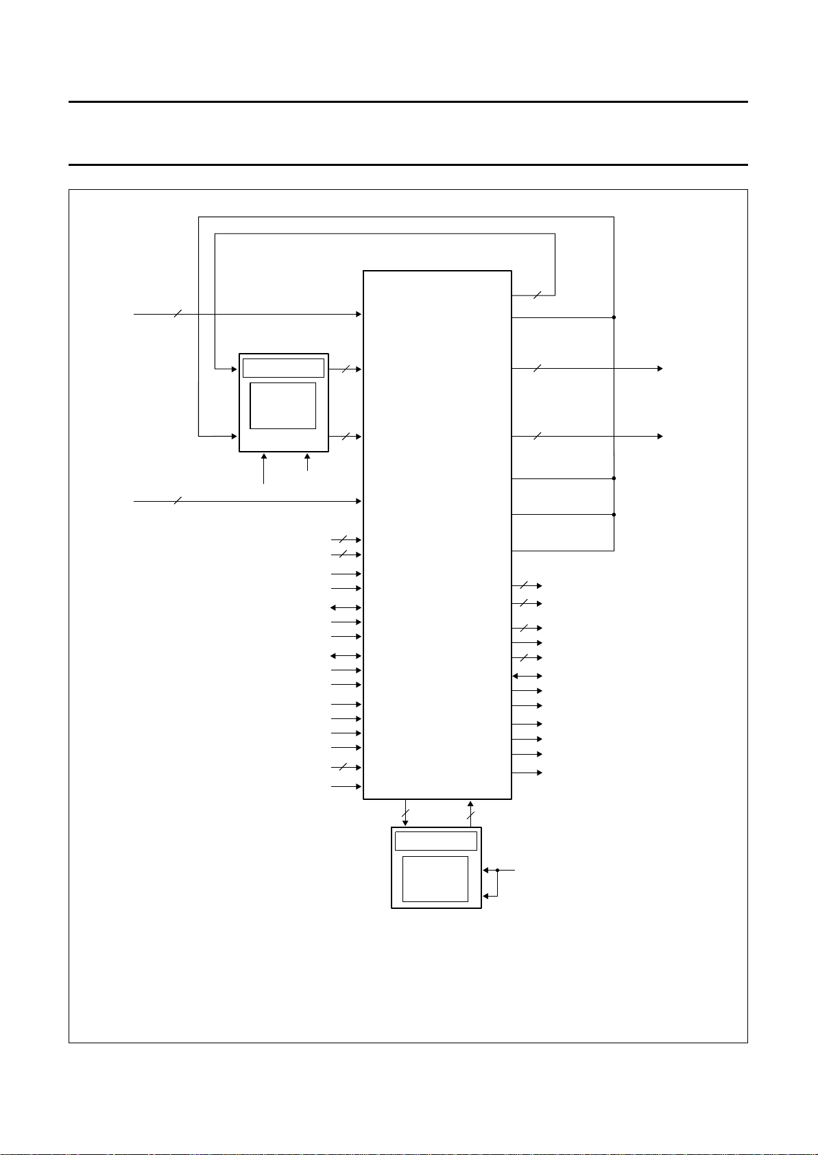
7.15 Control
The control part (see Fig.2) generates all necessary
internal control signals for the MACPACIC, the external
control signals for the field memories FM1 to FM4 and the
control signals for the VERIC. All of these signals are
derived from the mode bits transmitted via the SNERT
interface or from the reference input pins.
7.15.1 I
The horizontal reference signal is the rising edge of the
CLAMP input pulse generated by the 100 Hz memory
controller (see Fig.30). The rising edge of WE_FRONT
defines the first active horizontal sample of the incoming
data Y_FRONT. The vertical reference signal is the rising
edge of VA_FRONT (see Fig.32), derived from the
synchronisation IC (e.g. TDA9144).
For PALplus input signals line 24 is the first processed line
related to VA_FRONT. When MACP or standard input
signals are used, line 21 is the first processed line related
to VA_FRONT.
7.15.2 F
The acquisition line counter (ACQ) is preset with the
delayed rising edge of VA_FRONT (see Fig.2). With the
‘VA_FRONT Delay’ circuit it is possible to shift the rising
edge of VA_FRONT in multiples of CLK_16 clock periods.
This feature is necessary for unambiguous odd/even field
detection. The delay can be set via the SNERT interface.
The ACQ line counter is preset with logic 1 at the
beginning of the odd and even fields. The counter is
enabled with the rising edge of the clamp signal.
The display line counter (DSP) is used in the event of a
stand-alone MACPACIC (IVericN = 1) and is also preset
with the delayed rising edge of VA_FRONT. If VERIC is
available the field length measurement is active.
The display line counter is preset at the beginning of a
displayed odd and even field with the rising edge of VA_AI
set to logic 1.
NPUT REFERENCE SIGNALS
UNCTIONAL DESCRIPTION
SAA4996H
The rising edge of WE_FRONT marks the horizontal
location of the first active input data of MACPACIC.
The signal WE_MA defines the horizontal and vertical
active area in which the first field memory (FM5) of the
succeeding 100 Hz feature box stores incoming data.
The signal WE_MA is generated by comparing (via the
SNERT interface) the transmitted start and stop values
with the values of the display line counter and the pixel
counter 1.
The pixel counter 2 is preset with the rising edge of
WE_FRONT in such a way that the counter has the value
‘1’ when the first active input data pixel is valid at the
Y, UV_ADC input of MACPACIC. This counter is a 10-bit
modulo 1024 counter clocked with CLK_16I.
7.15.2.1 Memory control
The output of pixel counter 2 is used to generate the
horizontal read and write enable signals for FM1 and FM4
and the write enable signals for the field memories FM2
and FM3. The read cycle for FM2 and FM3 is controlled by
the VERIC.
The horizontal read and write signals are different for the
full PALplus module, for stand-alone MACPACIC and for
the odd and even fields. Therefore, the signals IVericN and
EVEN_FIELD are also input to the pixel decoder.
The output of the acquisition line counter is used to
generate the vertical part of the read and write enable
signals for FM1 and FM4 and the vertical part of the write
enable signals for the field memories FM2 and FM3.
The vertical read cycle for FM2 and FM3 is controlled by
the VERIC.
The horizontal and vertical component of the read and
write enable signals are different for the full PALplus
module and for the stand-alone MACPACIC. The line
values for the memory controlling are shown in Tables 6,
7 and 8.
The pixel counter 1 is preset with the rising edge of the
CLAMP pulse. The counter is clocked with the 16 MHz
clock signal CLK_16I.
1996 Oct 28 33

Philips Semiconductors Preliminary specification
Motion Adaptive Colour Plus And Control
IC (MACPACIC) for PALplus
handbook, full pagewidth
VIDEO
INPUT FROM
TDA9144
CLAMP
t
WE_F
WE_FRONT
SAA4996H
MHA144
t
: CLAMP phase to WE is programmable via SNERT-bus.
WE_F
Fig.30 Timing diagram of the horizontal reference input signals.
1996 Oct 28 34

Philips Semiconductors Preliminary specification
Motion Adaptive Colour Plus And Control
SAA4996H
IC (MACPACIC) for PALplus
Table 6 Pixel values for horizontal memory control
EVEN_FIELD IVericN H_WE_FM1 H_RE_FM1 H_WE_FM2 H_WE_FM3 H_WE_FM4 H_RE_FM4
0 0 0 to 839 −−−−−
0 1 2 to 841 24 to 863 −−−−
10−0 to 839 27 to 866 27 to 866 9 to 848 0 to 839
1 1 26 to 865 0 to 839 −−9to848 0to839
Table 7 Line values for vertical memory control, PALplus signals
EVEN_FIELD IVericN V_WE_FM1 V_RE_FM1 V_WE_FM2 V_WE_FM3 V_RE_FM4 V_WE_FM4
0 0 21 to 311 −−−−−
0 1 21 to 311 21 to 311 −−−−
10−20 to 310 24 to 59
167 to 274
1 1 22 to 312 20 to 310 −−21 to 311 21 to 311
Table 8 Line values for vertical memory control, MACP and standard signals
60 to 166
275 to 310
21 to 311 21 to 311
EVEN_FIELD IVericN V_WE_FM1 V_RE_FM1 V_WE_FM2 V_WE_FM3 V_RE_FM4 V_WE_FM4
0 0 21 to 311 −−−−−
0 1 21 to 311 21 to 311 −−−−
10−20 to 310 21 to 166 167 to 311 21 to 311 21 to 311
1 1 22 to 312 20 to 310 −−21 to 311 21 to 311
The horizontal and vertical memory control signals are
combined in the H/V logic to generate the memory read
and write signals.
In all modes, except the MultiPIP mode, the signal
VA_RES is used as a reset signal for the field memories
FM1 to FM4 (RSTW_FM23 and RST_FM14). If the
MultiPIP mode is selected, the signal VA_AI is an input
signal generated by an external memory controller. In this
event the signal VA_AI_DIFF is used as RSTW_FM23.
The signal WE_FM2 is set to logic 1 and all other read and
write enable signals are set to logic 0. If the stand-alone
MACPACIC and MultiPIP mode is selected, all memory
control signals are set to logic 0.
The output pins 46 to 48 have different output signals
depending on the environment in which MACPACIC is
used. If it is part of a full PALplus module these pins deliver
bits of chrominance data, in the stand-alone MACPACIC
mode they output memory control signals
(see Chapter “Pinning”). Selection of either mode is
performed by the control signal IVericN.
7.15.2.2 The output signal HREF_MA
The signal HREF_MA is generated by delaying the
CLAMP input signal two clocks CLK_16. The HREF_MA
signal is used in the VERIC as a clock pulse for the internal
line counter. The timing is illustrated in Fig.34.
7.15.2.3 VERIC control output signals
In the VERIC control decoder of MACPACIC the output
signals FILM and INTPOL are generated as shown in
Table 9.
1996 Oct 28 35

Philips Semiconductors Preliminary specification
Motion Adaptive Colour Plus And Control
SAA4996H
IC (MACPACIC) for PALplus
Table 9 Generation of the signals FILM and INTPOL
22Valid FilmOn Mpip HlpM0 HlpM1 FILM INTPOL
1000000
1000101
1001001
1001101
1100000
1100111
1101011
1101111
0000000
0000101
0001001
0001101
0100000
0100101
0101001
0101101
XX1XX10
7.15.2.4 Field length measurement
On the full PALplus module the field length is measured in
the MACPACIC.
The ACQ line counter counts the lines between two
succeeding vertical pulses. The one-line-long vertical
output signal VA_AI has a delay of 1.5 fields with respect
to the delayed VA_FRONT input signal and has the same
phase relationship to the CLAMP input signal for various
video input signals (VCR, NTSC).
For the stand-alone MACPACIC the 2.5 H signal
VA_FR_DEL is selected by the control signal IVericN as
the vertical reference output signal VA_AI.
7.15.2.5 Field detection
To detect the current odd or even field, the location of the
delayed VA_FRONT (VA_RES) input signal inside a line
has to be located.
For a PALplus video input signal the output signal
EVEN_FIELD is generated by enabling a register with the
VA_RES signal, which has the MSB of the pixel counter 2
at the D input.
In the bypass or MultiPIP mode the toggle function of the
register is active.
The odd/even field detection can be inverted by the
SNERT control bit InvO/E.
It is also possible to define the EVEN_FIELD signal by
software via a SNERT transmission.
7.15.2.6 Pins VA_FRONT and VA_AI
The signals VA_FRONT and VA_AI have bidirectional
functions. In all modes, except the MultiPIP mode, the pin
VA_FRONT is an input pin and the pin VA_AI is an output
pin. If the MultiPIP mode is selected the pin VA_AI is an
input pin and the signal is connected to the VA_FRONT pin
which now becomes an output pin (see Fig.2 and Fig.35).
7.15.3 SNERT
AN95XXX)
In the SNERT interface the external signals SNERT_CL
and SNERT_DA are processed to address and data.
A synchronisation to the bus performed with the reset
signal SNERT_RST. The transmitted data is valid with the
next rising edge of SNERT_RST.
The block diagram and the data, clock and reset timing of
the SNERT interface are shown in Fig.3 and Fig.36.
INTERFACE (SEE APPLICATION NOTE
1996 Oct 28 36

Philips Semiconductors Preliminary specification
Motion Adaptive Colour Plus And Control
IC (MACPACIC) for PALplus
7.15.3.1 Serial interface protocol
Power-on state: After power-on the serial interface is in
an unknown state. The information in the actual data
registers is random. When signals are applied to
SNERT_CL and SNERT_DA in this state, the behaviour is
unpredictable.
Initialization state: After power-on, or in any other state,
the initialization state is entered after the rising edge of the
signal SNERT_RST. The SNERT clock counter C1 is
reset with the rising edge of SNERT_RST. The data
registers remain loaded with the last transmitted values.
Address reception state: After reset the address
reception state is entered. On each negative edge of
SNERT_CL the next data bit from SNERT_DA is shifted
into the input shift register. The counter is incremented
with each rising edge of SNERT_CL. After the 8th negative
edge of SNERT_CL the Address Latch Enable (ALE)
pulse is generated. With this enable pulse the contents of
the shift register is loaded into the address register. If an
address in the range 50H to 64H, 67H or 68H is decoded,
one of the 8-bit wide input data registers is selected.
Data reception state: If a valid address is received, the
next eight bits on SNERT_DA are considered as data bits.
When the 8 data bits have been shifted into the shift
register the counter enables the loading of the data word
in one of the 23 data registers in combination with the
decoded address.
There are three data register banks;
• The actual data register bank
• The acquisition data register bank
• The synchronizing register bank.
After a SNERT transmission is completed another
SNRST pulse must follow in order to enable the
acquisition registers and make the data valid.
The synchronizing registers are enabled with the signals
‘line2_odd_every_field’ respectively ‘line2_every_field’,
which are related to the vertical reference input signal
VA_FRONT.
SAA4996H
7.15.3.2 Special SNERT transmission requirements
EVEN_FIELD definition:
After switching on the MACPACIC, the EVEN_FIELD
output signal toggles.
When the EVEN_FIELD signal accidentally toggles in the
right way (EVEN_FIELD = 0, odd field) and when a
PALplus input signal is present, the line 22 is detected.
Then the internal field detection is active and the normal
data processing starts up.
When the EVEN_FIELD signal toggles in the wrong way
(EVEN_FIELD = 0, even field), line 22 will never be
detected and the field detection remains in this wrong
behaviour.
Solution: After switching on the MACPACIC or after
switching into PALplus or MACP mode, the EVEN_FIELD
output signal has to be defined by the control bits
‘EnPreEvFld’ and ‘PreEvFld’ of the control 6 SNERT
register.
Luminance offset hysteresis control:
For luminance offset control a hysteresis function is
applied to the measured luminance offset. The hysteresis
function is controlled by the three black offset hysteresis
control bits BOH0, BOH1 and BOH2 transmitted via
SNERT (control 5 data register).
To guarantee the correct hysteresis function, the following
software actions are necessary:
First the hysteresis has to be set to zero via SNERT
(BOH = 0). After a PALplus input signal is detected (line 22
is valid), the actual black offset is measured in the next
frame. During this time (40 ms) the software remains in the
stand-by position. One of the possible hysteresis values
can then be transmitted via SNERT.
Data send state: If the transmitted address is 65H or 66H,
the ‘send_rcv’ signal defines the SNERT_DA pin as an
output and, with the positive edge of the next
8 SNERT_CL pulses generated by the microcontroller, the
data output register is read out.
1996 Oct 28 37

Philips Semiconductors Preliminary specification
Motion Adaptive Colour Plus And Control
IC (MACPACIC) for PALplus
SAA4996H
(2)
X
(2)
X
(2)
X
DATA BYTE
D7 D6 D5 D4 D3 D2 D1 D0
22Valid 623Valid 23Valid IVericN IMacpacicN
(1)
X
(1)
X
SelSdYl1 SelSdYl0 NmYl1 NmYl0 Rha/Rhb2 Rha/Rhb1 Rha/Rhb0
(1)
(1)
(2)
(2)
X
FUNCTION
(HEX)
7.15.3.3 Address and data overview
Table 10 Address and data overview
ADDRESS
Address 50H to 64H, 67H and 68H contains write data (data from microprocessor); address 65H and 66H contains read data (data to microcontroller).
1996 Oct 28 38
50 Control1 Preset MacpOn HlpM1 HlpM0 FilmOn MotVis1 MotVis0 InvO/E
51 Control2 Mpip VaDel2 VaDel1 VaDel0 FastTest WeShift16_1 WeShift16_0 EnIRXR
52 WeStrtH StrtH7 StrtH6 StrtH5 StrtH4 StrtH3 StrtH2 StrtH1 StrtH0
53 WeStpH StpH7 StpH6 StpH5 StpH4 StpH3 StpH2 StpH1 StpH0
54 WeStrtV0 StrtV07 StrtV06 StrtV05 StrtV04 StrtV03 StrtV02 StrtV01 StrtV00
55 WeStrtV1 StrtV17 StrtV16 StrtV15 StrtV14 StrtV13 StrtV12 StrtV11 StrtV10
56 WeStpV0 StpV07 StpV06 StpV05 StpV04 StpV03 StpV02 StpV01 StpV00
57 WeStpV1 StpV17 StpV16 StpV15 StpV14 StpV13 StpV12 StpV11 StpV10
58 HlpRedThr1 HlpThr17 HlpThr16 HlpThr15 HlpThr14 HlpThr13 HlpThr12 HlpThr11 HlpThr10
59 HlpRedThr2 HlpThr27 HlpThr26 HlpThr25 HlpThr24 HlpThr23 HlpThr22 HlpThr21 HlpThr20
5A HlpRedThr3 HlpThr37 HlpThr36 HlpThr35 HlpThr34 HlpThr33 HlpThr32 HlpThr31 HlpThr30
5B HlpRedThr4 HlpThr47 HlpThr46 HlpThr45 HlpThr44 HlpThr43 HlpThr42 HlpThr41 HlpThr40
5C HlpRedThr5 HlpThr57 HlpThr56 HlpThr55 HlpThr54 HlpThr53 HlpThr52 HlpThr51 HlpThr50
5D MacpYhThr1 MaThr17 MaThr16 MaThr15 MaThr14 MaThr13 MaThr12 MaThr11 MaThr10
60 IrxrThr1 IrxrThr17 IrxrThr16 IrxrThr15 IrxrThr14 IrxrThr13 IrxrThr12 IrxrThr11 IrxrThr10
5F MacpYhThr3 MaThr37 MaThr36 MaThr35 MaThr34 MaThr33 MaThr32 MaThr31 MaThr30
5E MacpYhThr2 MaThr27 MaThr26 MaThr25 MaThr24 MaThr23 MaThr22 MaThr21 MaThr20
61 IrxrThr2 IrxrThr27 IrxrThr26 IrxrThr25 IrxrThr24 IrxrThr23 IrxrThr22 IrxrThr21 IrxrThr20
62 IrxrThr3 IrxrThr37 IrxrThr36 IrxrThr35 IrxrThr34 IrxrThr33 IrxrThr32 IrxrThr31 IrxrThr30
63 IrxrThr4 IrxrThr47 IrxrThr46 IrxrThr45 IrxrThr44 IrxrThr43 IrxrThr42 IrxrThr41 IrxrThr40
64 FixHlpMain FixHlp3 FixHlp2 FixHlp1 FixHlp0 FixMain3 FixMain2 FixMain1 FixMain0
65 Control3 X
66 Control4 X
67 Control5 BOH2 BOH1 BOH0 VAA1 VAA0 SEL_SD_YL1 SEL_SD_YL0 NAIRXR
68 Control6 Interlace EnPreEvFld PreEvFld X
Notes
1. Bits not valid.
2. Don’t care (bits can be logic 0 or logic 1).

Philips Semiconductors Preliminary specification
Motion Adaptive Colour Plus And Control
IC (MACPACIC) for PALplus
7.15.3.4 Command explanation
Table 11 Control1
ADDRESS
(HEX)
50 W 7 Preset 0: normal processing
R/W BIT NAME FUNCTION
1: abandon the recursive measurement loops and load the circuits
with actual video data
6 MacpOn 0: Motion Adaptive Colour Plus decoding not activated
1: Motion Adaptive Colour Plus decoding activated
5, 4 HlpM1 and HlpM0 00: bypass mode VERIC
01: vertical up-conversion without use of helper
10: vertical enhancement with adaptive helper processing
11: vertical enhancement with helper amplitude and main
reference via SNERT interface
3 FilmOn 0: camera mode activated
1: film mode activated
2, 1 MotVis1 and MotVis0 00: don’t show motion decisions
01: show Y motion decisions
10: show C motion decisions
11: show M motion decisions
0 InvO/E 0: don’t invert EVEN_FIELD definition
1: invert EVEN_FIELD definition
SAA4996H
Table 12 Control2
ADDRESS
(HEX)
51 W 7 Mpip 0: MultiPIP mode not active
R/W BIT NAME FUNCTION
1: MultiPIP with the help of PIP module is activated; VA_AI is set
to input and VA_FRONT to output; the signal at the WE_FRONT
pin is used
6 to 4 VaDel2, VaDel1 and
VaDel0
3 FastTest 0: normal mode: activating new SNERT commands at frame
2, 1 WeShift16_1 and
WeShift16_0
0 EnIRXR 0: disable Intelligent Residual cross-luminance Reduction
internal delay of V A_FRONT in multiples of CLK_16 clock periods;
range: [0, 64, 128 to 448] CLK_16 periods; this feature is required
for unambiguous Odd/Even field detection
boundaries related to VA_FRONT (address 50H to 57H and 68H)
1: activating new SNERT commands immediately
shift of WE_MA of 0 to 3 16 MHz samples related to the positive
edge of CLAMP
1: enable Intelligent Residual cross-luminance Reduction
1996 Oct 28 39

Philips Semiconductors Preliminary specification
Motion Adaptive Colour Plus And Control
SAA4996H
IC (MACPACIC) for PALplus
Table 13 Programming of WE_MA
ADDRESS
(HEX)
52 W 7 to 0 WeStrtH distance between rising edge of CLAMP and rising edge of WE_MA in
53 W 7 to 0 WeStpH distance between rising edge of CLAMP and falling edge of WE_MA in
54 W 7 to 0 WeStrtV0 number of lines between rising edge of VA_AI (VA_FRONT) and first active
55 W 7 to 0 WeStrtV1
56 W 7 to 0 WeStpV0 number of lines between rising edge of VA_AI (VA_FRONT) and first
57 W 7 to 0 WeStpV1
WeStrtH, WeStpH, WeStrtV and WeStpV:
The horizontal reference is the rising edge of the CLAMP
signal. The vertical reference is the rising edge of the
VA_FRONT signal. This signal is set via software. Signals
WeStrtH and WeStpH define the horizontal active area.
Signals (WeStrtV0 and WeStrtV1) and
(WeStpV0 and WeStpV1) mark the vertical active area.
The least significant bit of the start and stop address is also
the most significant bit of the data.
R/W BIT NAME FUNCTION
multiples of 4 CLK_16 periods
multiples of 4 CLK_16 periods
WE_MA line
non-active WE_MA line
signals WeShift16_0 and WeShift16_1 shifts the active
horizontal area over 0 to 3 clock periods of 16 MHz. In this
case the positive as well as the negative edge will shift
over the same amount of samples.
WeStrtV0 indicates the vertical start addresses 1 to 256
and WeStrtV1 indicates the addresses 257 to 512.
The vertical start at line 1 is not allowed. WeStpV0
indicates the vertical stop addresses 1 to 256 and
WeStpV1 indicates the addresses 257 to 512.
Because the number of 16 MHz samples in a line is 1024,
and one data byte can only define 256 positions, the
horizontal start and stop positions are defined with a
4 MHz resolution. To reach the full 16 MHz resolution the
handbook, full pagewidth
WeStrtV
WeStpV
WeStrtH
If WeStrtH = WeStpH and WeStrtV0 = WeStpV0 or
WeStrtV1 = WeStpV1 the output control signal WE_MA is
switched to a LOW level and no data will be written into the
succeeding module (still picture).
WeStpH
MHA145
1996 Oct 28 40
Fig.31 Boundaries of the WE_MA signal.

Philips Semiconductors Preliminary specification
Motion Adaptive Colour Plus And Control
SAA4996H
IC (MACPACIC) for PALplus
Table 14 Helper Reduction Thresholds
ADDRESS
(HEX)
58 W 7 to 0 HlpRedThr1 5 thresholds defining the ranges in which the 5 modes for adaptive helper
59 W 7 to 0 HlpRedThr2
5A W 7 to 0 HlpRedThr3
5B W 7 to 0 HlpRedThr4
5C W 7 to 0 HlpRedThr5
Table 15 Definition of Y_HP Reduction Thresholds related to MACP
ADDRESS
(HEX)
5D W 7 to 0 MacpYhThr1 3 thresholds defining the ranges in which the 3 modes for adaptive Yhp
5E W 7 to 0 MacpYhThr2
5F W 7 to 0 MacpYhThr3
Table 16 Definition of Y_HP Reduction Thresholds related to PLL disturbances
R/W BIT NAME FUNCTION
reduction will be applied (inclusive hysteresis); this adaptivity prevents
from artefacts of helper noise break through
R/W BIT NAME FUNCTION
reduction will be applied (inclusive hysteresis)
ADDRESS
(HEX)
60 W 7 to 0 IrxrThr1 4 thresholds defining the ranges in which the 4 modes for the intelligent
61 W 7 to 0 IrxrThr2
62 W 7 to 0 IrxrThr3
63 W 7 to 0 IrxrThr4
Table 17 Definition of fixed helper gain and relative main amplitude (FixHlpMain)
ADDRESS
(HEX)
64 W 7 to 4 FixHlp3,
R/W BIT NAME FUNCTION
residual cross-luminance reduction will be applied; this adaptivity prevents
from artefacts caused by the PLL disturbance
R/W BIT NAME FUNCTION
definition of helper gain
FixHlp2,
FixHlp1,
FixHlp0
3 to 0 FixMain3,
FixMain2,
FixMain1,
FixMain0
definition of relative main amplitude (letter box)
1996 Oct 28 41

Philips Semiconductors Preliminary specification
Motion Adaptive Colour Plus And Control
IC (MACPACIC) for PALplus
Table 18 Control3
ADDRESS
(HEX)
65 R 7 to 5 X no function
R/W BIT NAME FUNCTION
4 22Valid 0: correct MACP and/or helper processing is not possible and is
automatically switched off; helpers are blanked and MACPACIC is forced
into camera mode; reference levels of line 22 are not valid
1: correct MACP and/or helper processing could be possible; reference
levels of line 22 are valid
3 623Valid 0: correct helper processing is not possible and is automatically switched
off; reference values of line 623 are not valid
1: correct helper processing could be possible; reference values of line 623
are valid
2 23Valid 0: correct helper processing is not possible and is automatically switched
off; reference values of line 23 are not valid
1: correct helper processing could be possible; reference values of line 23
are valid
1 IVericN 0: VERIC available
1: VERIC not available
0 IMacpacicN 0: MACPACIC available
1: MACPACIC not available
SAA4996H
Table 19 Control4
ADDRESS
(HEX)
66 R 7 X no function
R/W BIT NAME FUNCTION
6, 5 SelSdYl1,
SelSdYl0
4, 3 NmYl1,
NmYl0
2 to 0 Rha/Rhb2,
Rha/Rhb1,
Rha/Rhb0
indication of the Y_HP reduction factor, which is further saturation
dependent; these are deduced from the noise within full band (line 623)
indication of the Y_HP reduction factor deduced from the noise within the
helper (line 23)
indication of the amount of helper bandwidth reduction and helper amplitude
reduction; these are deduced from the noise within the helper (line 23)
1996 Oct 28 42

Philips Semiconductors Preliminary specification
Motion Adaptive Colour Plus And Control
IC (MACPACIC) for PALplus
Table 20 Control5
ADDRESS
(HEX)
67 W 7 to 5 BOH2, BOH1,
R/W BIT NAME FUNCTION
selection of black offset hysteresis:
BOH0
4, 3 VAA1 and
VAA0
2, 1 SEL_SD_YL1,
SEL_SD_YL0
0 NAIRXR 0: IRXR table selection dependent of SEL_SD_YL
000: 0
001: ±1
010: ±2
011: ±3
100: ±4
101: ±5
110: ±6
111: fixed black offset (51)
selection of the coefficients of the luminance vertical anti-alias filter
(DEC_Y_VAA): see Table 21
selection of IRXR characteristics (NAIRXR = 0): see Table 22
1: noise adaptive IRXR table selection
SAA4996H
Table 21 DEC_Y_VAA
VAA1 VAA0
0 0 odd 2 7 −1
0 0 even −17 2
01X242
10X323
11X404
Table 22 IRXR
SEL_SD_YL
0123456789ABCDEF
0 4432100000000000
1 4443210000000000
2 4444433221100000
3 4444444332210000
SELECTION OF THE LUMINANCE VERTICAL ANTI-ALIAS FILTER (DEC_Y_VAA)
FIELD COEFF1 COEFF2 COEFF3
SELECTION OF IRXR CHARACTERISTICS (NAIRXR = 0)
1996 Oct 28 43

Philips Semiconductors Preliminary specification
Motion Adaptive Colour Plus And Control
IC (MACPACIC) for PALplus
Table 23 Control6
ADDRESS
(HEX)
68 W 7 Interlace 0: incoming video signal is defined as ‘non interlaced’
8 TEST
8.1 Boundary scan test
Boundary Scan Test (BST) is supported. See boundary scan specification:
test access port and boundary scan architecture”.
8.1.1 IDENTIFICATION CODES
R/W BIT NAME FUNCTION
1: incoming video signal is defined as ‘interlaced’
6 EnPreEvFld 0: EVEN_FIELD signal defined internally
1: EVEN_FIELD signal defined by SNERT transmission: PreEvFld
5 PreEvFld 0: incoming field is defined as ‘Odd’
1: incoming field is defined as ‘Even’
4 to 0 X no function
“IEEE Standard 1149.1 - 1990, IEEE standard
SAA4996H
The PALplus ICs MACPACIC and VERIC are equipped with BST identification registers. The identification codes and
their meaning are shown in Tables 24 and 25.
Table 24 Identification codes
VERSION COMPONENT MANUFACTURER FIXED IDENTIFICATION
IC
MACPACIC 0001 01101 00001 00011 0 00000010101 1 1684602B
VERIC 0001 10110 00101 10010 0 00000010101 1 1B16402B
Table 25 Code parts
31 to 28 version number start with 1 and increment every redesign
27 to 12 component first 3 characters of name
11 to 1 manufacturer JEDEC code for PHILIPS
3322 22222 22211 11111 1 11000000000 0 −
1098 76543 21098 76543 2 10987654321 0 −
BITS NAME DESCRIPTION
0 fixed 1
1996 Oct 28 44

Philips Semiconductors Preliminary specification
Motion Adaptive Colour Plus And Control
IC (MACPACIC) for PALplus
helper
reference burst
bits
signalling
mid grey
odd field
set-up
black set-up
Z22
SAA4996H
MHA139
even field
handbook, full pagewidth
main white
reference
even field
main black
reference
H
helper signal
CVBS
2.5 H
Z1 Z2 Z3 Z4 Z5 Z6 Z23 Z24 Z25
H
1/2
Z622 Z623 Z624 Z625
Z621
Z620
video input signal
of TDA9144
VA_FRONT
VA_RES
odd field
CVBS
Z313 Z314 Z315 Z316 Z317 Z318 Z319 Z335 Z336 Z337Z308 Z309 Z310 Z311 Z312
VA_FRONT
Fig.32 Timing of the vertical synchronisation pulse (VA_FRONT) and the delayed vertical signal (VA_RES).
VA_RES
1996 Oct 28 45

Philips Semiconductors Preliminary specification
Motion Adaptive Colour Plus And Control
IC (MACPACIC) for PALplus
SAA4996H
MHA143
handbook, full pagewidth
CLK_16
CLAMP
159 011023102260 79 80 81 82 919918917 920 92101023
PC1
WE_F
t
WE_FRONT
1 837 839 840 841 95395201023 954 95521003 1004943 944 945 838
PC2
Y0 Y1 Y836 Y837 Y838 Y839
YUV_ADC
Fig.33 Pixel timing of the input signals CLAMP and WE_FRONT.
: CLAMP phase to WE_RES (WE_FRONT) is programmable via SNERT-bus
WE_F
t
1996 Oct 28 46

Philips Semiconductors Preliminary specification
Motion Adaptive Colour Plus And Control
IC (MACPACIC) for PALplus
SAA4996H
MHA142
Y838a Y838b Y839a Y839bY1a Y1b
Y0a Y0b
handbook, full pagewidth
60 x CLK_16
60 x CLK_16
CLP_HRMA
t
WE_D
t
PD
t
Fig.34 Pixel timing of the output signals HREF_MA and WE_MA (full PALplus module and stand-alone MACPACIC).
1996 Oct 28 47
CLK_32B3
CLK_16B2
CLAMP
HREF_MA
WE_FRONT
WE_MA
YUV_MA
: delay CLAMP to HREF_MA, 2 × CLK_16B2
: data write enable delay
: processing delay
CLP_HRMA
PD
WE_D
t
t
t

Philips Semiconductors Preliminary specification
Motion Adaptive Colour Plus And Control
IC (MACPACIC) for PALplus
SAA4996H
MHA141
234
312
156 157
handbook, full pagewidth
odd field even field
d_VA_FRONT
t
VA_FRONT
VA_FR_DEL
EVEN_FIELD
CLAMP
314
313 1 2 3 155
158
156 157
3
2
1313 1313
312
LC_ACQ
even field odd field
VA_AI
1.5 fields
: this delay is defined via SNERT-bus
Fig.35 Horizontal timing of the input signal VA_FRONT and the output signal VA_AI (full PALplus module, all input signals except MultiPIP).
d_VA_FRONT
t
1996 Oct 28 48

Philips Semiconductors Preliminary specification
Motion Adaptive Colour Plus And Control
IC (MACPACIC) for PALplus
D0 D1 D2 D3 D4 D5 D6 D7
LSB MSBdata
SAA4996H
MHA140
handbook, full pagewidth
SNERT_RST
SNERT_CL
A0 A1 A2 A3 A4 A5 A6 A7
LSB MSBaddress
SNERT_DA
1234567 8 91011121314150
Fig.36 SNERT interface; data, clock and reset timing.
0
≥3 µs ≥4 µs
xx
ALE
DLE
PEDGE_SNERT_CL
NEDGE_SNERT_CL
COUNTER_OUT
1996 Oct 28 49

Philips Semiconductors Preliminary specification
Motion Adaptive Colour Plus And Control
SAA4996H
IC (MACPACIC) for PALplus
9 DC CHARACTERISTICS
Tj= 0 to 125 °C unless otherwise specified.
SYMBOL PARAMETER CONDITIONS MIN. TYP. MAX. UNIT
Supply
V
DD
I
DD
I
DD(PD)
Inputs
V
IL
V
IH
I
I
Outputs and 3-state
V
OL
V
OH
Outputs Y_TO_FM1, UV_TO_FM1, Y_MA, UV_MA, WE_MA, HREF_MA, UV_TO_FM4, EVEN_FIELD, INTPOL,
FILM, RST_FM14, WE_FM1, RE_FM1, WE_FM4, RE_FM4 and CLK_16B1
I
OL
I
OH
Outputs CLK_32B1, CLK_32B2 and CLK_16B2
I
OL
I
OH
Outputs CLK_32B3 and CLK_16B3
I
OL
I
OH
3-state TDO_MA, SNERT_DA, VA_FRONT and VA_AI
I
Z
supply voltage 4.75 5.00 5.25 V
supply current − 80 − mA
quiescent supply current all inputs to VDD or V
−−100 µA
SS
LOW level input voltage 0 − 0.8 V
HIGH level input voltage 2.0 − V
DD
V
input current −−1.0 µA
LOW level output voltage IO=20µA −−0.1 V
HIGH level output voltage IO=20µAV
− 0.1 −−V
DD
LOW level output current VO= 0.5 V 4 −−mA
HIGH level output current VO=VDD− 0.5 V 4 −−mA
LOW level output current VO= 0.5 V 8 −−mA
HIGH level output current VO=VDD− 0.5 V 8 −−mA
LOW level output current VO= 0.5 V 12 −−mA
HIGH level output current VO=VDD− 0.5 V 12 −−mA
input current −−10 µA
1996 Oct 28 50

Philips Semiconductors Preliminary specification
Motion Adaptive Colour Plus And Control
IC (MACPACIC) for PALplus
handbook, full pagewidth
CLK
DATA
90 %
50 %
10 %
t
r
t
h
XX
t
oh
t
od
SAA4996H
t
f
t
l
Dn + 1Dn
t
ih
t
su
MHA146
Data input: CLK = CLK_16.
Data output: CLK = CLK_16 for stand-alone MACPACIC and CLK = CLK_32 for full PALplus module.
Fig.37 Clock to data timing.
10 AC CHARACTERISTICS
T
= 0 to 125 °C unless otherwise specified.
j
SYMBOL PARAMETER CONDITIONS MIN. TYP. MAX. UNIT
Clock CLK_32
T
cy
t
r
t
f
t
h
t
l
cycle time 28.1 −−ns
rise time 2 − 4ns
fall time 2 − 4ns
HIGH time 9.2 −−ns
LOW time 9.2 −−ns
Clock CLK_16
T
CY
t
r
t
f
t
h
t
l
cycle time 56.2 −−ns
rise time 2 − 4ns
fall time 2 − 4ns
HIGH time 20.5 −−ns
LOW time 20.5 −−ns
Input set-up time
t
su
set-up time all data inputs 6 −−ns
CLK_16 w.r.t. CLK_32 4.5 −−ns
1996 Oct 28 51

Philips Semiconductors Preliminary specification
Motion Adaptive Colour Plus And Control
SAA4996H
IC (MACPACIC) for PALplus
SYMBOL PARAMETER CONDITIONS MIN. TYP. MAX. UNIT
Input hold time
t
ih
Outputs (C
CLK_16B1, CLK_16B2
t
oh
t
od
CLK_16B1, CLK_16B2 AND CLK_16B3 (FALLING)
t
oh
t
od
CLK_32B1, CLK_32B2 AND CLK_32B3 (RISING)
t
oh
t
od
CLK_32B1, CLK_32B2 AND CLK_32B3 (FALLING)
t
oh
t
od
Outputs YUV_TO_FM1, RST_FM14, WE_FM1, RE_FM1, WE_FM4, RE_FM4, HREF_MA, WE_MA, VA_AI,
VA_FRONT and YUV_MA (CLK_16; C
t
oh
t
od
Outputs (CLK_32; C
input hold time all data inputs 3 −−ns
CLK_16 w.r.t. CLK_32 3.5 −−ns
= 15 pF)
L
AND CLK_16B3 (RISING)
hold time 6 −−ns
delay time −−17 ns
hold time 9 −−ns
delay time −−24 ns
hold time 6 −−ns
delay time −−17 ns
hold time 6 −−ns
delay time −−17 ns
= 15 pF)
L
hold time 12 −−ns
delay time −−38 ns
= 15 pF; note 1)
L
YUV_MA
t
oh
t
od
hold time 13 −−ns
delay time −−39 ns
RSTW_FM23, WE_FM2 AND WE_FM3
t
oh
t
od
hold time 12 −−ns
delay time −−38 ns
Note
1. 32 MHz output signals are related to the output clock signals CLK_32B1 and CLK_32B3.
10.1 Clock buffers
MACPACIC supplies the clocks for VERIC and the field memories on the PALplus module. Therefore the input clocks
CLK_16 and CLK_32 are buffered and output as CLK_16B1 to CLK_16B3 and CLK_32B1 to CLK_32B3. The clock
distribution is shown in Fig.5.
1996 Oct 28 52

Philips Semiconductors Preliminary specification
Motion Adaptive Colour Plus And Control
IC (MACPACIC) for PALplus
11 LIST OF ABBREVIATIONS
Table 26 Abbreviations used in document
SYMBOL DESCRIPTION
ALE Address Latch Enable
BB Black Bands (above and below letter box picture)
BOH Black Offset Hysteresis (see Table 20)
CLP_DIFF Positive Edge of CLAMP Signal
DLE Data Latch Enable
EnlRXR Enable IRXR (see Table 12)
EnPreEvFld Enable Preset Even Field (see Table 23)
FixHlpMain Fix gain of Helper and Main Amplitude (see Table 17)
HlpM Helper mode (see Table 11)
HlpRedThr Helper Reduction Threshold (see Table 14)
H_RE/WE Horizontal part of Read Enable/Write Enable signal
InvO/E Invert Odd/Even
IRXR Intelligent Residual Cross-Luminance Reduction
IrxrThr IRXR Threshold (see Table 16)
IVericN VERIC Identification (active LOW) (see Table 18)
LC_ACQ Acquisition Line Counter
LC_DSP Display Line Counter
MACP Motion Adaptive Colour Plus
MacpOn MACP on (see Table 11)
MacpYhThr MACP Luminance Threshold (see Table 15)
MotVis Motion Visibility (see Table 11)
Mpip MultiPIP (see Table 12)
NmYl Noise Dependent Luminance High-Pass Reduction (see Table 19)
PreEvFld Preset Even Field (see Table 23)
Rha/Rhb Helper Bandwidth and Amplitude Reduction (see Table 19)
SEL_SD_YL Select Saturation Dependent Cross-Luminance Reduction (see Table 22)
VAA Vertical Anti-Alias Filter (see Table 21)
VA_AI_DIFF Positive Edge of VA_AI
VaDel Delay of VA_FRONT
VA_FR_DEL VA_FRONT Delayed
V_RE/WE Vertical part of Read Enable/Write Enable signal
WeStrtH Horizontal Start and Stop values for WE_MA (see Table 13 and Fig.31)
WeStpH
WeStrtV Vertical Start and Stop values for WE_MA (see Table 13 and Fig.31)
WeStpV
XL Cross-Luminance
Y_HP Luminance High-Pass Component
Y_LP Luminance Low-Pass Component
SAA4996H
1996 Oct 28 53

Philips Semiconductors Preliminary specification
Motion Adaptive Colour Plus And Control
IC (MACPACIC) for PALplus
12 PACKAGE OUTLINE
QFP100: plastic quad flat package;
100 leads (lead length 1.95 mm); body 14 x 20 x 2.7 mm; high stand-off height
c
y
X
80 51
81
50
A
Z
E
SAA4996H
SOT317-1
pin 1 index
100
1
w M
b
0.25
p
D
H
D
cE
0.25
0.13
D
20.1
19.9
p
0.40
0.25
0 5 10 mm
(1)
(1) (1)(1)
14.1
13.9
e
DIMENSIONS (mm are the original dimensions)
mm
A
max.
3.3
0.36
0.10
2.87
2.57
UNIT A1A2A3b
Note
1. Plastic or metal protrusions of 0.25 mm maximum per side are not included.
30
Z
D
scale
eH
H
24.2
0.65
23.6
31
D
e
H
E
w M
b
p
v M
A
B
v M
B
LLpQZywv θ
E
18.2
17.6
1.0
0.6
A
2
A
E
1.43
1.23
A
1
detail X
0.151.95 0.10.2
Q
(A )
3
θ
L
p
L
Z
E
D
1.0
0.6
o
7
o
0
0.8
0.4
OUTLINE
VERSION
SOT317-1
1996 Oct 28 54
REFERENCES
IEC JEDEC EIAJ
EUROPEAN
PROJECTION
ISSUE DATE
92-11-17
95-02-04

Philips Semiconductors Preliminary specification
Motion Adaptive Colour Plus And Control
IC (MACPACIC) for PALplus
13 SOLDERING
13.1 Introduction
There is no soldering method that is ideal for all IC
packages. Wave soldering is often preferred when
through-hole and surface mounted components are mixed
on one printed-circuit board. However, wave soldering is
not always suitable for surface mounted ICs, or for
printed-circuits with high population densities. In these
situations reflow soldering is often used.
This text gives a very brief insight to a complex technology.
A more in-depth account of soldering ICs can be found in
our
“IC Package Databook”
13.2 Reflow soldering
Reflow soldering techniques are suitable for all QFP
packages.
The choice of heating method may be influenced by larger
plastic QFP packages (44 leads, or more). If infrared or
vapour phase heating is used and the large packages are
not absolutely dry (less than 0.1% moisture content by
weight), vaporization of the small amount of moisture in
them can cause cracking of the plastic body. For more
information, refer to the Drypack chapter in our
Reference Handbook”
Reflow soldering requires solder paste (a suspension of
fine solder particles, flux and binding agent) to be applied
to the printed-circuit board by screen printing, stencilling or
pressure-syringe dispensing before package placement.
Several techniques exist for reflowing; for example,
thermal conduction by heated belt. Dwell times vary
between 50 and 300 seconds depending on heating
method. Typical reflow temperatures range from
215 to 250 °C.
(order code 9398 652 90011).
“Quality
(order code 9398 510 63011).
SAA4996H
If wave soldering cannot be avoided, the following
conditions must be observed:
• A double-wave (a turbulent wave with high upward
pressure followed by a smooth laminar wave)
soldering technique should be used.
• The footprint must be at an angle of 45° to the board
direction and must incorporate solder thieves
downstream and at the side corners.
Even with these conditions, do not consider wave
soldering the following packages: QFP52 (SOT379-1),
QFP100 (SOT317-1), QFP100 (SOT317-2),
QFP100 (SOT382-1) or QFP160 (SOT322-1).
During placement and before soldering, the package must
be fixed with a droplet of adhesive. The adhesive can be
applied by screen printing, pin transfer or syringe
dispensing. The package can be soldered after the
adhesive is cured.
Maximum permissible solder temperature is 260 °C, and
maximum duration of package immersion in solder is
10 seconds, if cooled to less than 150 °C within
6 seconds. Typical dwell time is 4 seconds at 250 °C.
A mildly-activated flux will eliminate the need for removal
of corrosive residues in most applications.
13.4 Repairing soldered joints
Fix the component by first soldering two diagonallyopposite end leads. Use only a low voltage soldering iron
(less than 24 V) applied to the flat part of the lead. Contact
time must be limited to 10 seconds at up to 300 °C. When
using a dedicated tool, all other leads can be soldered in
one operation within 2 to 5 seconds between
270 and 320 °C.
Preheating is necessary to dry the paste and evaporate
the binding agent. Preheating duration: 45 minutes at
45 °C.
13.3 Wave soldering
Wave soldering is not recommended for QFP packages.
This is because of the likelihood of solder bridging due to
closely-spaced leads and the possibility of incomplete
solder penetration in multi-lead devices.
1996 Oct 28 55

Philips Semiconductors Preliminary specification
Motion Adaptive Colour Plus And Control
SAA4996H
IC (MACPACIC) for PALplus
14 DEFINITIONS
Data sheet status
Objective specification This data sheet contains target or goal specifications for product development.
Preliminary specification This data sheet contains preliminary data; supplementary data may be published later.
Product specification This data sheet contains final product specifications.
Limiting values
Limiting values given are in accordance with the Absolute Maximum Rating System (IEC 134). Stress above one or
more of the limiting values may cause permanent damage to the device. These are stress ratings only and operation
of the device at these or at any other conditions above those given in the Characteristics sections of the specification
is not implied. Exposure to limiting values for extended periods may affect device reliability.
Application information
Where application information is given, it is advisory and does not form part of the specification.
15 LIFE SUPPORT APPLICATIONS
These products are not designed for use in life support appliances, devices, or systems where malfunction of these
products can reasonably be expected to result in personal injury. Philips customers using or selling these products for
use in such applications do so at their own risk and agree to fully indemnify Philips for any damages resulting from such
improper use or sale.
1996 Oct 28 56
 Loading...