


INTEGRATED CIRCUITS
DATA SH EET
For a complete data sheet, please also download:
•The IC04 LOCMOS HE4000B Logic
Family Specifications HEF, HEC
•The IC04 LOCMOS HE4000B Logic
Package Outlines/Information HEF, HEC
HEF4753B
LSI
Universal timer module
Product specification
File under Integrated Circuits, IC04
January 1995
Philips Semiconductors Product specification
Universal timer module
DESCRIPTION
The HEF4753B is a universal timer module for counting
and dividing as well as for event-recognition and
manipulation of input sequences.
The following functions are included: synchronization and
edge-detection of the input signal, programmable counter,
clock divider with different lengths, operating mode
decoder, control logic and output multiplexer.
Depending on the operating mode and the application, the
circuit works as a presettable 8-bit counter with
HEF4753B
LSI
transient-pulse suppression, pulse duration selector
divider, counter, positive or negative edge delaying
module or low-frequency control circuit.
All manipulation possibilities depend on a time scaling,
which is adjustable by the 8-bit programmable counter and
the system clock. The system clock can be divided
internally by 1, 16, 256 or 4096 as input clock for the
counter. In all cases the manipulated input sequence
appears at the only output OUT.
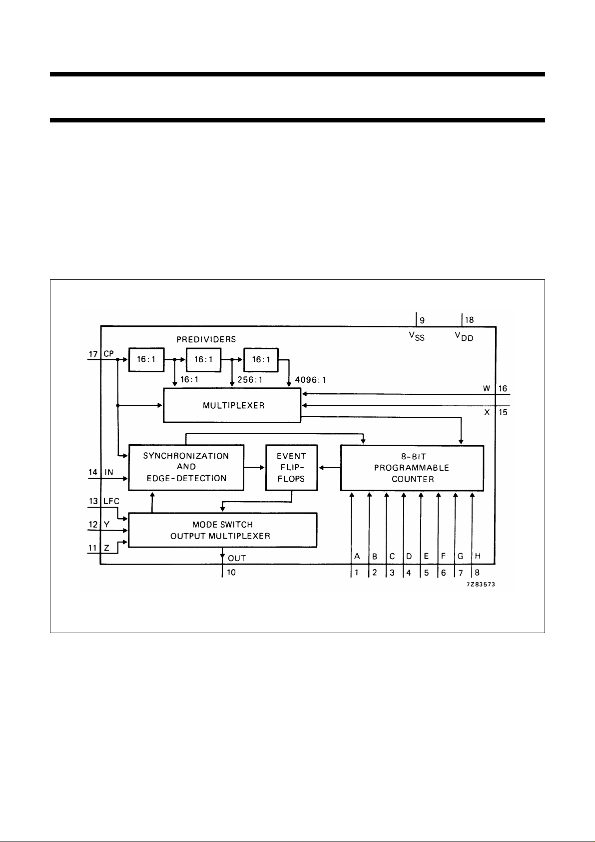
Fig.1 Functional diagram.
FAMILY DATA, IDDLIMITS category LSI
See Family Specifications
January 1995 2
Philips Semiconductors Product specification
Universal timer module
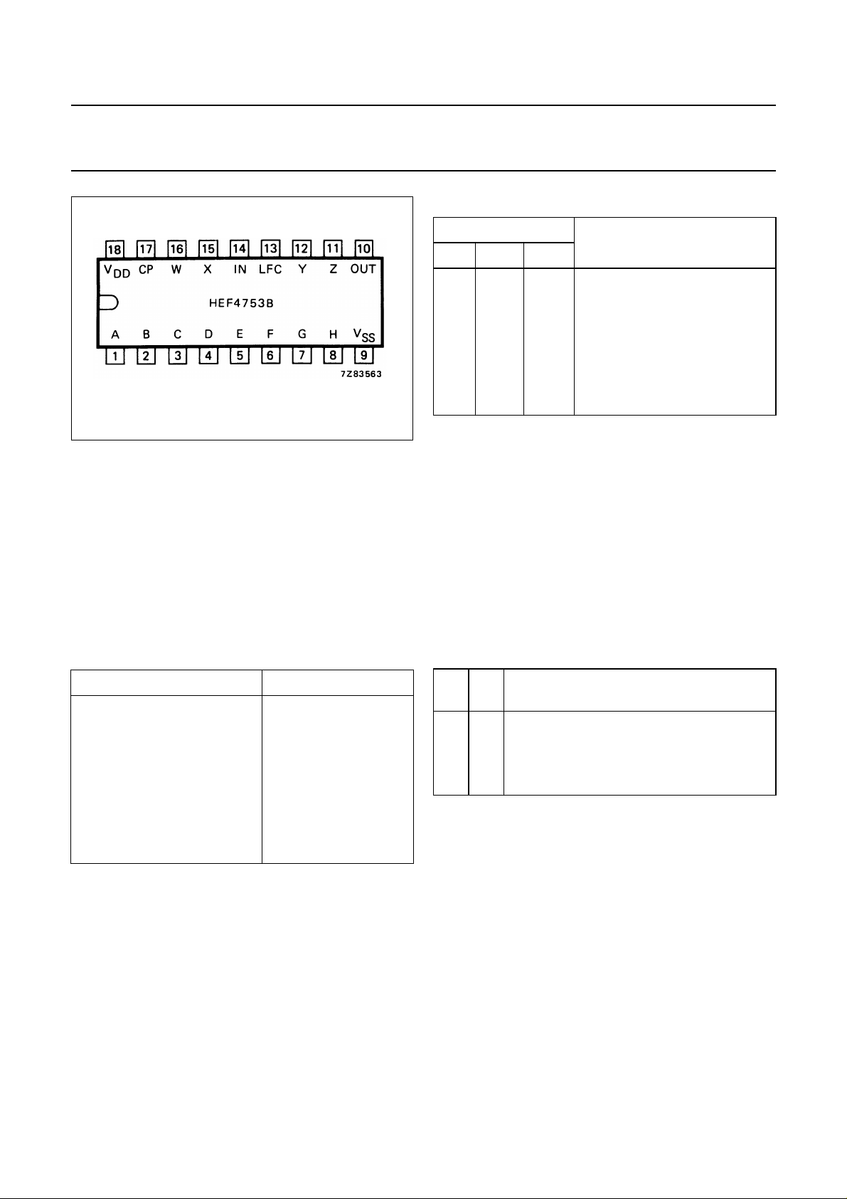
Fig.2 Pinning diagram.
HEF4753BP(N): 18-lead DIL; plastic
(SOT102-3)
HEF4753BD(N): 18-lead DIL; ceramic (cerdip)
(SOT133)
( ): Package Designator North America
HEF4753B
LSI
FUNCTION TABLES
INPUTS
OPERATING MODE
LFC Y Z
L L H counter
L H L divider
H H L delayed LOW to HIGH edge
H L H delayed HIGH to LOW edge
H H H transient pulse suppression
L H H frequency recognition
LFC L L digital pulse duration selector
Notes
1. H = HIGH state (the more positive voltage).
2. L = LOW state (the less positive voltage).
Programmable 8-bit counter
INPUTS ACTIVE LOW VALUE
A1
B2
C4
D8
E16
F32
G64
H 128
Note
1. All inputs A to H HIGH is not allowed.
(1)
12-bit predivider
WX
L L X=1
L H X =16
H L X = 256
H H X = 4096
CLOCK FOR PROGRAMMABLE
COUNTER CP/X
January 1995 3

Philips Semiconductors Product specification
Universal timer module
FUNCTIONAL DESCRIPTION
Clock divider and decoder
The clock signal at input CP is, at its original frequency, the
system clock, but it also drives the programmable counter.
The counter input frequency can be predivided by the
factors 1/16, 1/256 and 1/4096, depending on the logic
state of inputs W and X (according to the function tables
above).
8-bit programmable counter
The 8 inputs A to H are the set inputs of the 8 counter
flip-flops. The setting is triggered by an edge of the input
signal (at input IN) depending on of the chosen mode.
Event flip-flops, synchronization and edge-detection
The event flip-flops are used to recognize the positive
and/or negative edge of the input signal at IN.
Parts of the flip-flops are used together with the
programmable 8-bit counter as a retriggerable mono-flop,
which defines the time scaling for event recognition.
The input IN is synchronized by the clock signal CP.
HEF4753B
LSI
Mode switch and output multiplexer
This function switches the chosen output to the output
(OUT) and gives the mode of which the edge at input IN
has to be detected. The inputs Z, Y and LFC give 7 modes
+1, that means in mode ‘Digital Filter’ the input LFC can be
HIGH or LOW.
OPERATING MODES
The circuit has 6 operating modes which are activated by
the logic state of inputs LFC, Y and Z. An extra mode is
possible by using two circuits which are connected such so
they function as a digital band-filter.
1. Counter mode (LFC = LOW; Y = LOW; Z = HIGH) In this mode the output OUT should be connected to input
IN. If not, only one counter cycle starts after a transition at
input IN (see Fig.3 and note 1.).
A B C D E F G H W X LFC Y Z
HH L H H H HHL L L L H
Fig.3 Timing diagram for counter mode; t1= delay until set of 8-bit counter; t2= delay to set 8-bit counter;
t3= predefined delay by programming.
January 1995 4

Philips Semiconductors Product specification
Universal timer module
HEF4753B
LSI
2. Divider mode (LFC = LOW; Y = HIGH; Z = LOW) In this mode the output OUT should be connected to input IN. If not, only one counter cycle starts after a transition at
input IN (see Fig.4 and note 1.).
A B C D E F G H W X LFC Y Z
LLHHHHHHLLL HL
Fig.4 Timing diagram for divider mode; t1= delay until set of 8-bit counter; t2, t3see Fig.3.
3. Delayed LOW to HIGH edge mode; see note 2. (LFC = HIGH; Y = HIGH; Z = LOW)
ABCDEF GHWXLFCY Z
HLHHHHHHLL H H L
Fig.5 Timing diagram for delayed LOW to HIGH edge mode; t1= delay until set of 8-bit counter; t2= delay to
set 8-bit counter; t3= predefined delay by programming; t4= delay until next negative clock edge;
t5= delay until next positive clock edge.
January 1995 5

Philips Semiconductors Product specification
Universal timer module
4. Delayed HIGH to LOW edge mode; see note 2. (LFC = HIGH; Y = LOW; Z = HIGH)
A B C D E F G H W X LFC Y Z
HLHHHHHHLL H LH
HEF4753B
LSI
Fig.6 Timing diagram for delayed HIGH to LOW edge mode; for t1to t5see Fig.5.
5. Transient pulse suppression and pulse delaying mode; see note 2.(LFC=Y=Z=HIGH)
In this mode the circuit is working as a digital low-pass filter. An undisturbed pulse will only be delayed (see Fig.7).
A B C D E F G H W X LFC Y Z
LLHHHHHHLL H HH
Fig.7 Timing diagram for transient pulse suppression and pulse delaying mode; for t1,t2and t3see Fig.5.
January 1995 6

Philips Semiconductors Product specification
Universal timer module
HEF4753B
LSI
6. Frequency recognition mode (LFC = LOW; Y = HIGH; Z = HIGH) The incoming signal must be symmetrical within the limits as given by the specified delay time in note 2., to achieve lower
or higher frequency detection (see Fig.8).
A B C D E F G H W X LFC Y Z
LH L H HHH H L L L H H
Minimum dividing number is 3.
Fig.8 Timing diagram for frequency recognition mode; tx= time shorter than t3(OUT = H); ty= time greater than
t3(OUT = L); for t1, t2and t3see Fig.5.
January 1995 7

Philips Semiconductors Product specification
Universal timer module
HEF4753B
LSI
7. Digital pulse duration selector mode (Y = Z = LOW) This mode is a combination of two circuits, both used for frequency recognition. Both circuits are driven by the same clock
and same input signal, but programmed for different frequencies. The LFC input of the low-frequency circuit is set to logic
LOW, the output is connected to the LFC input of the high-frequency circuit, whose output (OUT) is the ‘filter’ output. The
delay time depends on the same facts as given in note 2.. For timing diagram see Fig.9.
A B C D E F G H W X LFC Y Z
LLLHHHHHLL L HHIC1
LLHHHHHHLL
Minimum dividing number is 3.
OUT
(IC1)
L L IC2
Fig.9 Timing diagram for digital pulse duration selector mode; t
t1= predefined delay by programming IC1; t2= predefined delay by programming IC2.
Notes to operating modes
1. The number of clocks for one cycle in the counter and divider mode is:
a. Contents of programmable counter plus one if X = W = LOW.
b. Contents of programmable counter multiplied by 16, 256 or 4096 if X and/or W = HIGH.
2. The delay in the modes 3, 4, 6 and 7, and the delay which is identical to the maximum duration of the transient pulse
in mode 5 depend on the optional divided clock frequency, the input conditions of the 8-bit presetable counter and in
addition, different times of propagation delays, jitter and maximum one half of a clock frequency period.
January 1995 8
IN1
, t
IN2
and t
are the IN input pulse durations;
IN3

Philips Semiconductors Product specification
Universal timer module
HEF4753B
DC CHARACTERISTICS
V
=0 V
SS
T
(°C)
amb
V
V
DD
V
Output (sink) 4,75 0,4 2,7 − 2,3 − 1,8 − mA
current LOW 10 0,5 I
(pin 10) 15 1,5 24,0 − 20,0 − 16,0 − mA
Output (source) 5 4,6 0,6 − 0,5 − 0,4 − mA
current HIGH 10 9,5
(pin 10) 15 13,5 6,0 − 5,0 − 4,0 − mA
AC CHARACTERISTICS
V
SS
= 0 V; T
=25°C; CL= 50 pF; input transition times ≤ 20 ns
amb
V
DD
V
Propagation delays 5 420 850 ns
CP → OUT 10 t
HIGH to LOW 15 120 250 ns
5 450 900 ns
LOW to HIGH 10 t
15 140 280 ns
Output transition 5 30 60 ns
times 10 t
HIGH to LOW 15 10 20 ns
5 60 120 ns
LOW to HIGH 10 t
15 20 40 ns
Input rise and 5
pins 13, 14, 17 15
Maximum clock 5 3 6 MHz
pulse frequency 10 f
pins 17; δ = 50% 15 8 17 MHz
V
OH
OL
V
SYMBOL
V
−40 + 25 + 85
MIN. MAX. MIN. MAX. MIN. MAX.
OL
−I
OH
9,5 − 8,0 − 6,3 − mA
1,8 − 1,5 − 1,2 − mA
SYMBOL MIN. TYP. MAX.
PHL
PLH
THL
TLH
, t
r
max
f
7 14 MHz
180 360 ns
200 400 ns
15 30 ns
30 60 ns
no limitfall times 10 t
TYPICAL EXTRAPOLATION
FORMULA
LSI
January 1995 9

Philips Semiconductors Product specification
Universal timer module
V
DD
V
Dynamic power 5 1 800 f
dissipation per 10 8 000 f
package (P) 15 19 000 f
TYPICAL FORMULA FOR P (µW)
+∑(foCL) × V
i
+∑(foCL) × V
i
+∑(foCL) × V
i
DD
DD
DD
HEF4753B
LSI
2
2
2
where
fi= input freq. (MHz)
fo= output freq. (MHz)
C
= load capacitance (pF)
L
∑ (f
) = sum of outputs
oCL
= supply voltage (V)
V
DD
January 1995 10
 Loading...