


INTEGRATED CIRCUITS
DATA SH EET
For a complete data sheet, please also download:
•The IC04 LOCMOS HE4000B Logic
Family Specifications HEF, HEC
•The IC04 LOCMOS HE4000B Logic
Package Outlines/Information HEF, HEC
HEF4534B
LSI
Real time 5-decade counter
Product specification
File under Integrated Circuits, IC04
January 1995
Philips Semiconductors Product specification
Real time 5-decade counter
DESCRIPTION
The HEF4534B is a 5-decade ripple counter. The binary
outputs of the decade counters are time-multiplexed by an
internal scanner on four BCD outputs (O0to O3). The
selected decade is indicated by a logic HIGH on the
appropriate digit select output (OS0: units, 1; OS1: tens,
10; OS2: hundreds, 102;OS3: thousands, 103; OS4: ten
thousands, 104).
The binary outputs (O0to O3) and the select outputs
(OS0to OS4) are 3-state controlled via enable inputs
EO and EOS respectively, allowing interface with other
bus orientated devices. Cascading may be accomplished
by using the carry out (TC). The counter is triggered by a
LOW to HIGH transition on the decade clock (CPA) and is
reset by a HIGH level on the master reset (MR). The
HEF4534B
LSI
scanner is triggered by a LOW to HIGH transition on the
scanner clock (CPS) and is reset (select ten thousand
counter) by a HIGH level on the scanner reset (MR
The counter can operate in four modes depending on the
state of the mode select inputs (SA,SB). The error detector
will detect an error when a positive edge on CPA is not
accompanied by a negative edge on the error detector
clock CPE or vice versa, within time limits adjusted by
external capacitors connected to C
ext 1
and C
ext 2.
more detected errors result in a HIGH level on the error
output (OER). The error detector is reset by a HIGH level
on MR.
Schmitt-trigger action in the clock inputs makes the circuit
highly tolerant to slower clock rise and fall times.
).
sc
Three or
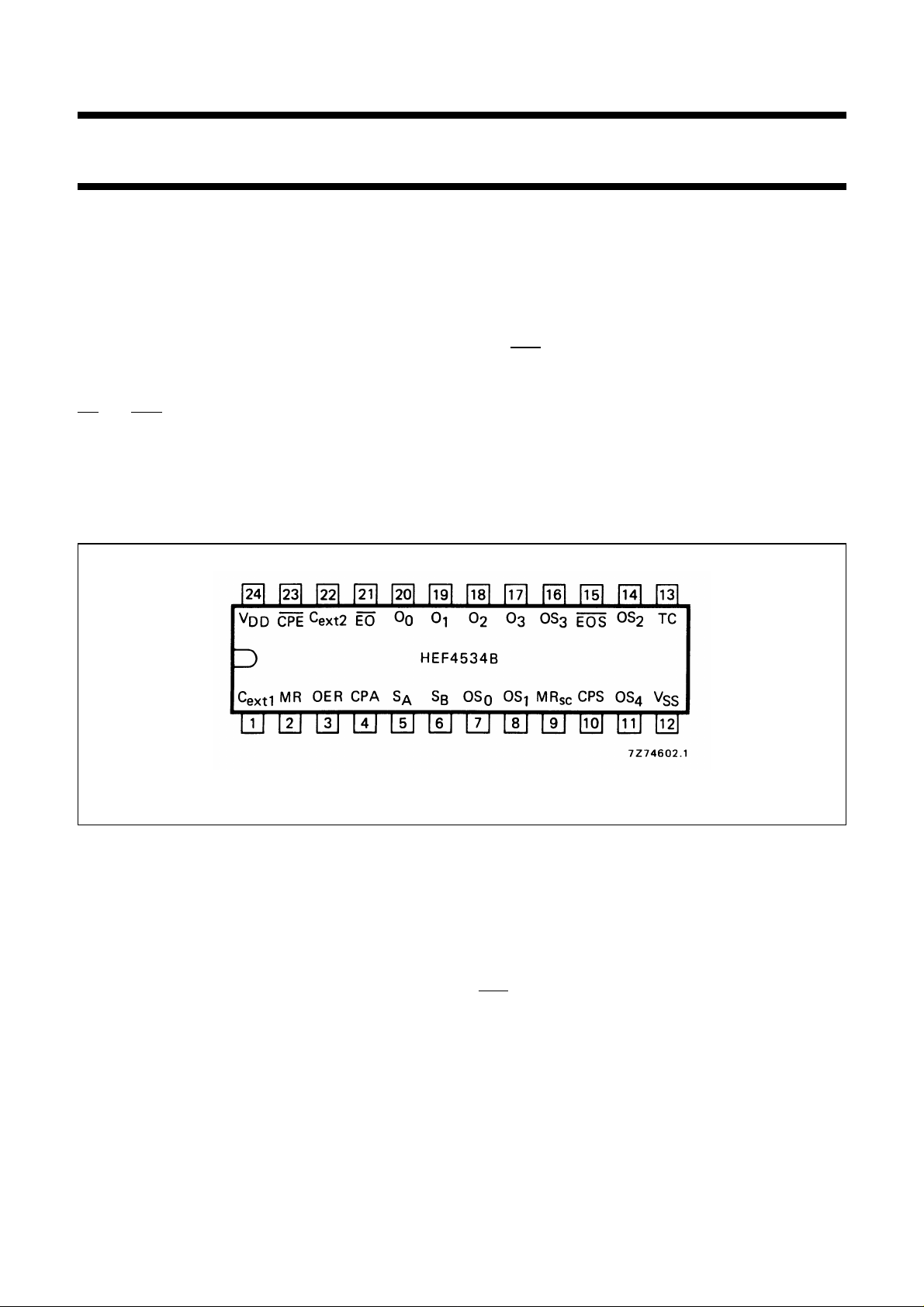
Fig.1 Pinning diagram.
HEF4534BP(N): 24-lead DIL; plastic (SOT101-1)
HEF4534BD(F): 24-lead DIL; ceramic (cerdip) (SOT94)
HEF4534BT(D): 24-lead SO; plastic (SOT137-1)
( ): Package Designator North America
January 1995 2
PINNING
O
OS
1
to O
to OS
0
3
3
BCD outputs
digit select outputs
OER error output
CPA decade clock input
CPS scanner clock input
CPE error detector clock input
S
A,SB
mode select inputs
MR master reset input
MR
sc
scanner reset input
TC carry out
FAMILY DATA, I
LIMITS category LSI
DD
See Family Specifications
Philips Semiconductors Product specification
Real time 5-decade counter
HEF4534B
LSI
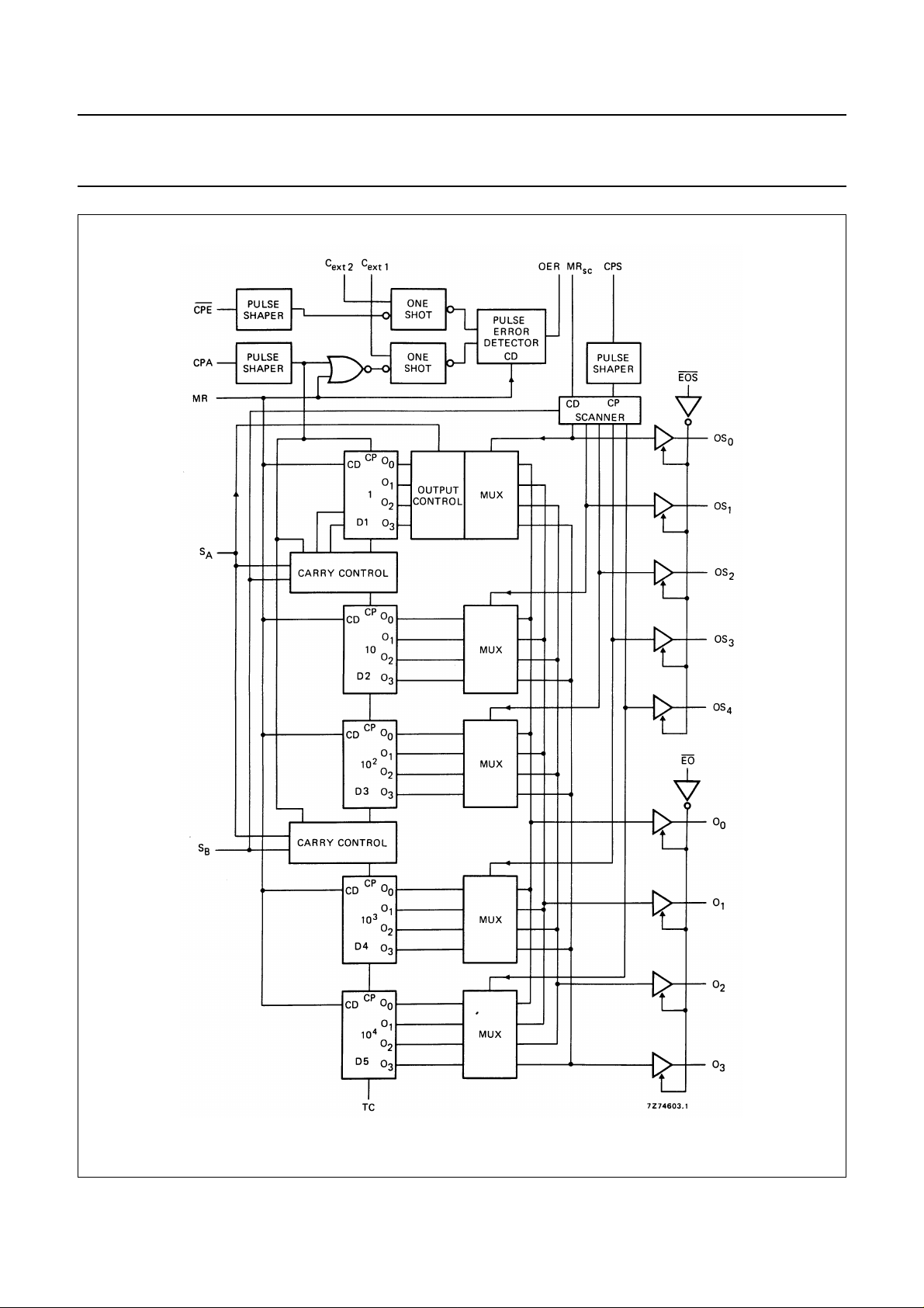
Fig.2 Functional block diagram.
January 1995 3

Philips Semiconductors Product specification
Real time 5-decade counter
MODE CONTROL FUNCTION TABLE
SELECT INPUTS 1ST DECADE
S
A
S
B
LL
OUTPUT
normal count at 9 to 0 transition at 9 to 0 transition 5-decade
and display of the 1st decade of the 3rd decade counter
L H inhibited input clock input clock
H H inhibited
display counts:
HL
3, 4, 5, 6, 7 = 5
8, 9, 0, 1, 2 = 0
CARRY TO 2ND STAGE CARRY TO 4TH STAGE MODE
at 4 to 5 transition
of the 1st decade
at 7 to 8 transition
of the 1st decade
at 9 to 0 transition
of the 3rd decade
at 9 to 0 transition
of the 3rd decade
HEF4534B
LSI
test purposes:
clock directly into
stages 1, 2 and 4
4-decade counter
with ÷ 10 and roundoff at front end
4-decade counter;
1
⁄2-pence capability
Fig.3 Error detection timing diagram.
The skew time is the time difference between the LOW to
HIGH transition of CPA and the HIGH to LOW transition of
CPE or vice versa (see Fig.4). The skew time is typically
proportional to the external capacitor (C
from C
ext1
and C
(pins 1 and 22) to VSS. The error
ext2
) connected
ext
detector will count an error when a positive edge on the
counter clock CPA is not succeeded by a negative edge on
Fig.4 Skew times
timing diagram;
t
> t
> t
SK1
SK2
;
.
WCPA
t
WCPE
January 1995 4
the error detector clock CPE within a skew time
t
(adjustable by C
SK1
at pin 1). The same holds for a
ext1
negative edge at CPE succeeded by a positive on CPA
within a skew time t
(adjustable by C
SK2
at pin 22). If
ext2
error detection is not needed,CPE must be either HIGH or
LOW and no C
is applied. For further information see
ext
Fig.5.

Philips Semiconductors Product specification
Real time 5-decade counter
HEF4534B
LSI
Note 1: Skew in this area results in counted error.
Note 2: Skew in the area between max. and min. curves may or may not result in counted error.
Note 3: Skew in this area results in no error counted.
Fig.5 Typical clock skew as a function of the supply voltage. This graph is accurate for C
T
=25°C.
amb
≥ 100 pF and
ext
Fig.6 Carry timing diagram.
January 1995 5

Philips Semiconductors Product specification
Real time 5-decade counter
HEF4534B
LSI
Note: If SB= H, the 1st decade is inhibited and the cycle will be shortened to four stages (see dotted lines).
Fig.7 Scanner timing diagram.
Fig.8 Counter timing diagram.
January 1995 6

Philips Semiconductors Product specification
Real time 5-decade counter
HEF4534B
AC CHARACTERISTICS
V
= 0 V; T
SS
Propagation delays
CPA → O
D1 selected 10 t
HIGH to LOW 15 95 190 ns 87 ns + (0,16 ns/pF) C
LOW to HIGH 10 t
CPA → O
D5 selected 10 t
HIGH to LOW 15 170 340 ns 162 ns + (0,16 ns/pF) C
LOW to HIGH 10 t
CPA → TC 5 420 840 ns 393 ns + (0,55 ns/pF) C
LOW to HIGH 10 t
MR → O
HIGH to LOW 10 t
MR → OER 5 140 280 ns 113 ns + (0,55 ns/pF) C
HIGH to LOW 10 t
CPS → O
HIGH to LOW 10 t
LOW to HIGH 10 t
CPS → OS
HIGH to LOW 10 t
CPS → OS
LOW to HIGH 10 t
=25°C; CL= 50 pF; input transition times ≤ 20 ns
amb
V
DD
V
n
SYMBOL MIN. TYP. MAX.
5 300 600 ns 283 ns + (0,55 ns/pF) C
PHL
5 240 480 ns 213 ns + (0,55 ns/pF) C
PLH
15 75 150 ns 67 ns + (0,16 ns/pF) C
n
5 550 1100 ns 523 ns + (0,55 ns/pF) C
PHL
5 550 1100 ns 523 ns + (0,55 ns/pF) C
PLH
15 170 340 ns 162 ns + (0,16 ns/pF) C
PLH
15 140 280 ns 132 ns + (0,16 ns/pF) C
n
5 200 400 ns 173 ns + (0,55 ns/pF) C
PHL
15 60 120 ns 52 ns + (0,16 ns/pF) C
PHL
15 50 100 ns 42 ns + (0,16 ns/pF) C
n
5 225 450 ns 198 ns + (0,55 ns/pF) C
PHL
15 70 140 ns 62 ns + (0,16 ns/pF) C
5 225 450 ns 198 ns + (0,55 ns/pF) C
PLH
15 70 140 ns 62 ns + (0,16 ns/pF) C
n
5 170 340 ns 143 ns + (0,55 ns/pF) C
PHL
15 50 100 ns 42 ns + (0,16 ns/pF) C
n
5 170 340 ns 143 ns + (0,55 ns/pF) C
PLH
15 50 100 ns 42 ns + (0,16 ns/pF) C
TYPICAL EXTRAPOLATION
FORMULA
130 260 ns 119 ns + (0,23 ns/pF) C
100 200 ns 89 ns + (0,23 ns/pF) C
230 460 ns 219 ns + (0,23 ns/pF) C
230 460 ns 219 ns + (0,23 ns/pF) C
190 380 ns 179 ns + (0,23 ns/pF) C
85 170 ns 74 ns + (0,23 ns/pF) C
65 130 ns 54 ns + (0,23 ns/pF) C
95 190 ns 84 ns + (0,23 ns/pF) C
95 190 ns 84 ns + (0,23 ns/pF) C
70 140 ns 59 ns + (0,23 ns/pF) C
70 140 ns 59 ns + (0,23 ns/pF) C
LSI
L
L
L
L
L
L
L
L
L
L
L
L
L
L
L
L
L
L
L
L
L
L
L
L
L
L
L
L
L
L
L
L
L
January 1995 7

Philips Semiconductors Product specification
Real time 5-decade counter
HEF4534B
V
DD
V
SYMBOL MIN. TYP. MAX.
Output transition times 5 60 120 ns 10 ns + (1,0 ns/pF) C
HIGH to LOW 10 t
THL
30 60 ns 9ns + (0,42 ns/pF) C
15 20 40 ns 6ns + (0,28 ns/pF) C
5 60 120 ns 10 ns + (1,0 ns/pF) C
LOW to HIGH 10 t
TLH
30 60 ns 9ns + (0,42 ns/pF) C
15 20 40 ns 6ns + (0,28 ns/pF) C
AC CHARACTERISTICS
V
= 0 V; T
SS
=25°C; CL= 50 pF; input transition times ≤ 20 ns
amb
V
DD
V
SYMBOL MIN. TYP. MAX.
3-state propagation delays
Output disable times
EO → On; 5 30 60 ns
EOS → OS
n
10 t
PHZ
25 50 ns
HIGH 15 20 40 ns
54080ns
LOW 10 t
PLZ
25 50 ns
15 20 40 ns
Output enable times
EO → On; 5 35 70 ns
EOS → OS
n
10 t
PZH
20 40 ns
HIGH 15 15 30 ns
5 50 100 ns
LOW 10 t
PZL
25 50 ns
15 15 30 ns
Minimum clock pulse 5 70 35 ns
width; CPA, CPS 10 t
WCPH
40 20 ns
HIGH 15 30 15 ns
Minimum reset pulse 5 90 45 ns
width; MR, MR
sc
10 t
WMRH
60 30 ns
HIGH 15 40 20 ns
Recovery time 5 120 60 ns
for MR 10 t
RMR
60 30 ns
15 50 25 ns
Recovery time 5 60 30 ns
for MR
sc
10 t
RMR
40 20 ns
15 30 15 ns
TYPICAL EXTRAPOLATION
FORMULA
LSI
L
L
L
L
L
L
January 1995 8

Philips Semiconductors Product specification
Real time 5-decade counter
V
DD
V
Maximum clock 5 2,5 5 MHz
pulse frequency 10 f
CPA and CPS 15 8 16 MHz
Dynamic power 5 1 100 f
dissipation per 10 4 800 f
package (P)
(1)
Note
1. C
ext
=0.
SYMBOL MIN. TYP. MAX.
max
V
DD
V
TYPICAL FORMULA FOR P (µW)
6 12 MHz
+∑(foCL) × V
i
+∑(foCL) × V
i
15 12 000 fi+∑(foCL) × V
DD
DD
DD
2
2
2
HEF4534B
where
fi= input freq. (MHz)
fo= output freq. (MHz)
= load cap. (pF)
C
L
∑ (f
) = sum of outputs
oCL
V
= supply voltage (V)
DD
LSI
January 1995 9

Philips Semiconductors Product specification
Real time 5-decade counter
HEF4534B
APPLICATION INFORMATION
Fig.9 Two HEF4534B ICs connected for cascade operation. TC is HIGH for a single clock period when all five
BCD decades go to zero. TC also goes HIGH when MR is applied.
LSI
Fig.10 Forcing a decade to the Onoutputs. When the Onoutputs of a given decade are required, this
configuration will lock-up the selected decade within four clock cycles. The select line feed back may be
hardwired or switched.
January 1995 10
 Loading...