INTEGRATED CIRCUITS
DATA SH EET
For a complete data sheet, please also download:
•The IC04 LOCMOS HE4000B Logic
Family Specifications HEF, HEC
•The IC04 LOCMOS HE4000B Logic
Package Outlines/Information HEF, HEC
HEF4531B
MSI
13-input parity checker/generator
Product specification
File under Integrated Circuits, IC04
January 1995

Philips Semiconductors Product specification
13-input parity checker/generator
DESCRIPTION
The HEF4531B is a parity checker/generator with 13 parity
inputs (I0to I12) and a parity output (O). When the number
of parity inputs that are HIGH is even, the output is LOW.
When the number of parity inputs that are HIGH is odd, the
output is HIGH. For words of 12 bits or less, the output can
be used to generate either odd or even parity by
appropriate termination of the unused parity input(s). For
words of 14 or more bits, the devices can be cascaded by
connecting the output of one device to any parity input of
another device. When cascading devices, it is
recommended that the output of one device be connected
to the I
to the output from the I12input than from any other input
(I0to I11).
input of the other device since there is less delay
12
HEF4531B
MSI
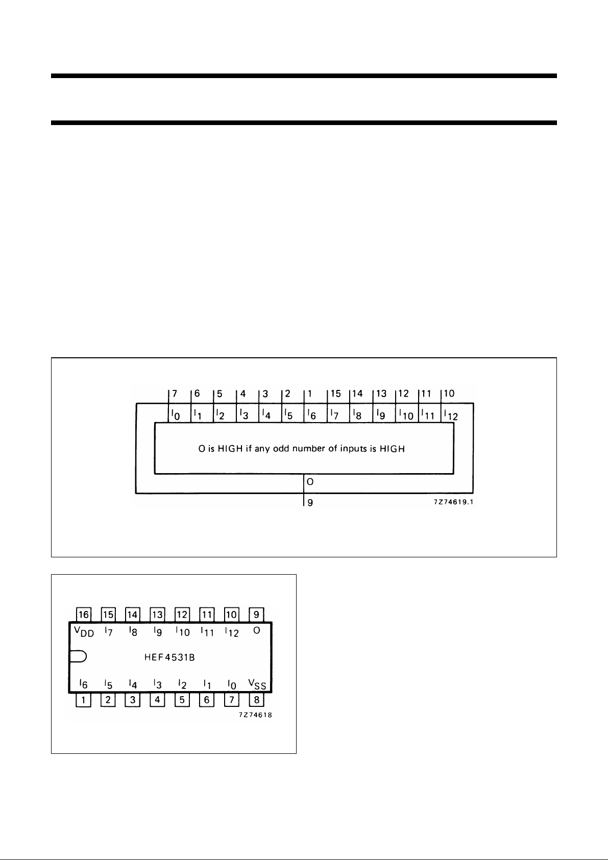
Fig.1 Functional diagram.
Fig.2 Pinning diagram.
January 1995 2
HEF4531BP(N): 16-lead DIL; plastic
(SOT38-1)
HEF4531BD(F): 16-lead DIL; ceramic (cerdip)
(SOT74)
HEF4531BT(D): 16-lead SO; plastic
(SOT109-1)
( ): Package Designator North America
FAMILY DATA, IDDLIMITS category MSI
See Family Specifications

Philips Semiconductors Product specification
13-input parity checker/generator
HEF4531B
MSI
Fig.3 Logic diagram.
FUNCTION TABLE
INPUTS OUTPUT
I
I
I
I
I
I
I
I
I
I
0
1
2
3
4
5
6
7
8
I
9
10I11I12
LLLLLLLLLLLLL L
any odd number of inputs HIGH H
any even number of inputs HIGH L
HHHHHHHHHHHHH H
Notes
1. H = HIGH state (the more positive voltage)
2. L = LOW state (the less positive voltage)
AC CHARACTERISTICS
= 0 V; T
V
SS
Dynamic power 5 425 f
dissipation per 10 2 400 f
package (P) 15 7 700 f
=25°C; input transition times ≤ 20 ns
amb
V
DD
V
TYPICAL FORMULA FOR P (µW)
+∑(foCL) × V
i
+∑(foCL) × V
i
+∑(foCL) × V
i
DD
DD
DD
2
2
2
where
fi= input freq. (MHz)
fo= output freq. (MHz)
C
= load capacitance (pF)
L
∑ (f
oCL
V
= supply voltage (V)
DD
O
) = sum of outputs
January 1995 3

Philips Semiconductors Product specification
13-input parity checker/generator
HEF4531B
AC CHARACTERISTICS
V
= 0 V; T
SS
Propagation delays
I0to I11→ O 5 145 290 ns 118 ns + (0,55 ns/pF) C
HIGH to LOW 10 t
LOW to HIGH 10 t
I12→ 0 5 105 210 ns 78 ns + (0,55 ns/pF) C
HIGH to LOW 10 t
LOW to HIGH 10 t
Output transition times 5 60 120 ns 10 ns + (1,0 ns/pF) C
HIGH to LOW 10 t
LOW to HIGH 10 t
=25°C; CL= 50 pF; input transition times ≤ 20 ns
amb
V
DD
V
SYMBOL TYP. MAX.
PHL
15 45 90 ns 37 ns + (0,16 ns/pF) C
5 135 270 ns 108 ns + (0,55 ns/pF) C
PLH
15 45 90 ns 37 ns + (0,16 ns/pF) C
PHL
15 35 70 ns 27 ns + (0,16 ns/pF) C
5 85 170 ns 58 ns + (0,55 ns/pF) C
PLH
15 25 50 ns 17 ns + (0,16 ns/pF) C
THL
15 20 40 ns 6 ns + (0,28 ns/pF) C
5 60 120 ns 10 ns + (1,0 ns/pF) C
TLH
15 20 40 ns 6 ns + (0,28 ns/pF) C
TYPICAL EXTRAPOLATION
FORMULA
60 120 ns 49 ns + (0,23 ns/pF) C
55 110 ns 44 ns + (0,23 ns/pF) C
45 90 ns 34 ns + (0,23 ns/pF) C
35 70 ns 24 ns + (0,23 ns/pF) C
30 60 ns 9 ns + (0,42 ns/pF) C
30 60 ns 9 ns + (0,42 ns/pF) C
MSI
L
L
L
L
L
L
L
L
L
L
L
L
L
L
L
L
L
L
January 1995 4
 Loading...