

Page 1
ZXTN2011G
100V NPN LOW SATURATION MEDIUM POWER LOW SATURATION
TRANSISTOR IN SOT223
SUMMARY
= 100V : R
BV
CEO
DESCRIPTION
Packaged in the SOT223 outline this new low saturation 100V NPN transistor
offers extremely low on state losses making it ideal for use in DC-DC circuits
and various driving and power management functions.
FEATURES
6 amps continuous current
•
Up to 10 amps peak current
•
Very low saturation voltages
•
APPLICATIONS
•
Motor driving
= 36m ; IC= 6A
SAT
3
2
2
T
O
S
•
Line switching
•
High side switches
•
Subscriber line interface cards (SLIC)
ORDERING INFORMATION
DEVICE REEL
SIZE
ZXTN2011GTA 7” 12mm
ZXTN2011GTC 13” 4,000 units
TAPE
WIDTH
embossed
QUANTITY PER
REEL
1,000 units
DEVICE MARKING
ZXTN
2011
ISSUE 1 - JUNE 2005
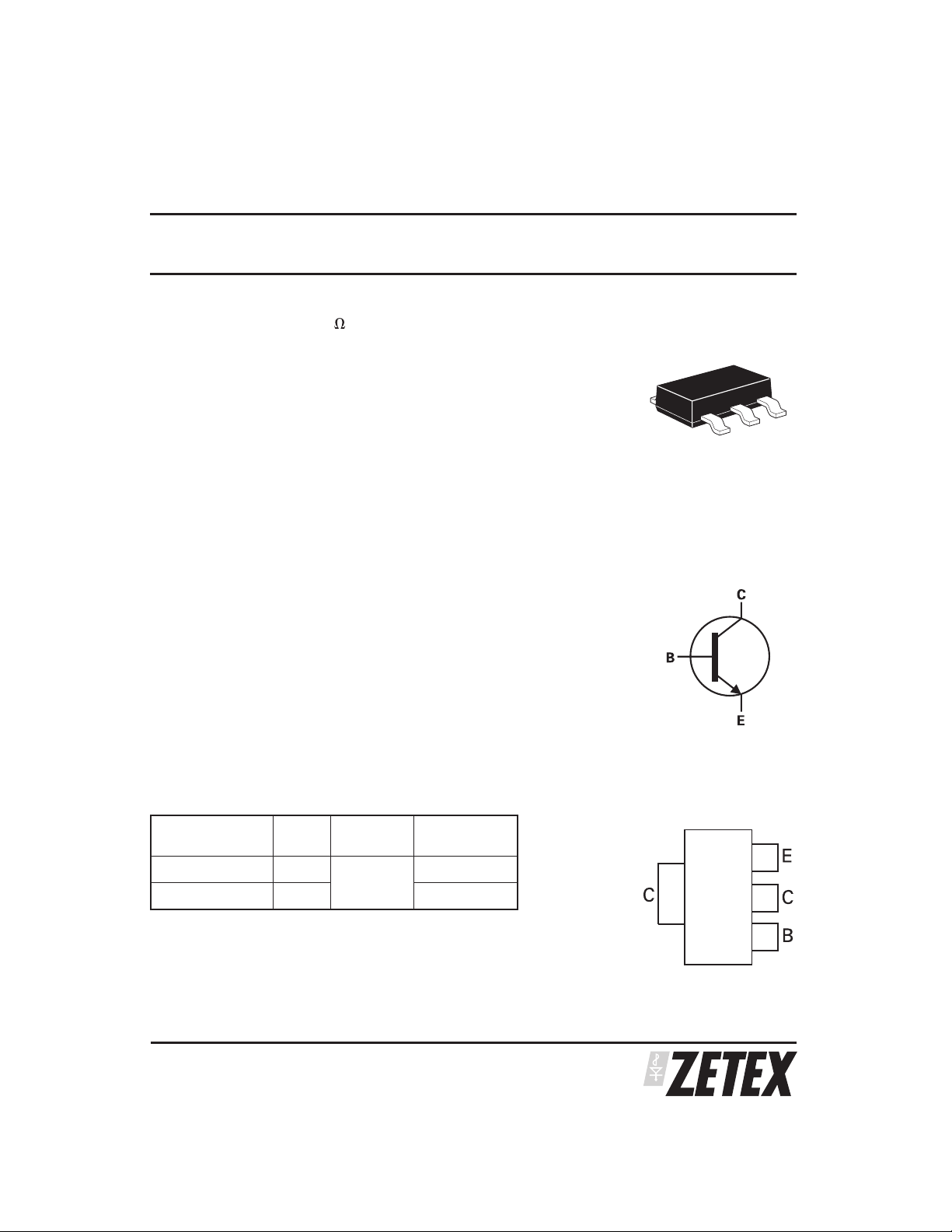
PINOUT
TOP VIEW
1
SEMICONDUCTORS
Page 2
ZXTN2011G
ABSOLUTE MAXIMUM RATINGS
PARAMETER SYMBOL LIMIT UNIT
Collector-base voltage BV
Collector-emitter voltage BV
Emitter-base voltage BV
Continuous collector current
(a)
Peak pulse current I
(a)
Power dissipation at T
=25°C
A
CBO
CEO
EBO
I
C
CM
P
D
Linear derating factor
Power dissipation at T
=25°C
A
(b)
P
D
Linear derating factor
Operating and storage temperature range T
j,Tstg
THERMAL RESISTANCE
PARAMETER SYMBOL VALUE UNIT
Junction to ambient
NOTES
(a) For a device surface mounted on 52mm x 52mm x 1.6mm FR4 PCB with high coverage of single sided 2oz copper, in still air conditions.
(b) For a device surface mounted on 25mm x 25mm x 1.6mm FR4 PCB with high coverage of single sided 1oz copper, in still air conditions.
(a)
R
⍜JA
200 V
100 V
7V
6 A
10 A
3.0
24
1.6
12.8
W
mW/°C
W
mW/°C
-55 to +150 °C
42 °C/W
SEMICONDUCTORS
ISSUE 1 - JUNE 2005
2
Page 3

CHARACTERISTICS
ZXTN2011G
ISSUE 1 - JUNE 2005
3
SEMICONDUCTORS
Page 4

ZXTN2011G
ELECTRICAL CHARACTERISTICS (at T
= 25°C unless otherwise stated)
amb
PARAMETER SYMBOL MIN. TYP. MAX. UNIT CONDITIONS
Collector-base breakdown voltage BV
Collector-emitter breakdown voltage BV
Collector-emitter breakdown voltage BV
Emitter-base breakdown voltage BV
Collector cut-off current I
Collector cut-off current I
R ⱕ 1k⍀
Emitter cut-off current I
Collector-emitter saturation voltage V
Base-emitter saturation voltage V
Base-emitter turn-on voltage V
Static forward current transfer ratio H
Transition frequency f
CBO
CER
CEO
EBO
CBO
CER
EBO
CE(SAT)
BE(SAT)
BE(ON)
FE
T
200 235 V IC=100A
200 235 V IC=1A, RBⱕ1k⍀
100 115 V IC=10mA*
78.1 VIE=100A
20
0.5nAA
20
0.5nAA
VCB=150V
=150V,T
V
CB
V
=150V
CB
=150V,T
V
CB
10 nA VEB=6V
21
35
mV
IC=0.1A, IB=5mA*
50
95
180
65
125
220
mV
mV
mV
I
I
I
=1A, IB=100mA*
C
=2A, IB=100mA*
C
=5A, IB=500mA*
C
1020 1120 mV IC=5A, IB=500mA*
920 1000 mV IC=5A, VCE=2V*
100
100
30
10
230
200
60
20
300
IC=10mA, VCE=2V*
=2A, VCE=2V*
I
C
=5A, VCE=2V*
I
C
=10A, VCE=2V*
I
C
130 MHz IC=100mA, VCE=10V
f=50MHz
Output capacitance C
Switching times t
t
OBO
ON
OFF
26 pF VCB=10V, f=1MHz*
41
1010
ns IC=1A, VCC=10V,
=100mA
I
B1=IB2
amb
amb
=100⬚C
=100⬚C
* Measured under pulsed conditions. Pulse width ⱕ 300s; duty cycle ⱕ2%.
SEMICONDUCTORS
4
ISSUE 1 - JUNE 2005
Page 5

TYPICAL CHARACTERISTICS
ZXTN2011G
ISSUE 1 - JUNE 2005
5
SEMICONDUCTORS
Page 6

ZXTN2011G
PAD LAYOUT DETAILSPACKAGE OUTLINE
Controlling dimensions are in millimeters. Approximate conversions are given in inches
PACKAGE DIMENSIONS
DIM
Millimeters Inches
Min Max Min Max Min Max Min Max
DIM
A - 1.80 - 0.071 e 2.30 BSC 0.0905 BSC
A1 0.02 0.10 0.0008 0.004 e1 4.60 BSC 0.181 BSC
b 0.66 0.84 0.026 0.033 E 6.70 7.30 0.264 0.287
b2 2.90 3.10 0.114 0.122 E1 3.30 3.70 0.130 0.146
C 0.23 0.33 0.009 0.013 L 0.90 - 0.355 D 6.30 6.70 0.248 0.264 - ----
Millimeters Inches
© Zetex Semiconductors plc 2005
Europe
Zetex GmbH
Streitfeldstraße 19
D-81673 München
Germany
Telefon: (49) 89 45 49 49 0
Fax: (49) 89 45 49 49 49
europe.sales@zetex.com
These offices are supported by agents and distributors in major countries world-wide.
Thispublicationisissuedtoprovideoutlineinformationonlywhich(unlessagreedbytheCompanyinwriting)maynotbeused,appliedorreproduced
for any purpose orform part of any order or contractor be regarded as a representation relatingto the products or services concerned. TheCompany
reserves the right to alter without notice the specification, design, price or conditions of supply of any product or service.
For the latest product information, log on to www.zetex.com
Americas
Zetex Inc
700 Veterans Memorial Hwy
Hauppauge, NY 11788
USA
Telephone: (1) 631 360 2222
Fax: (1) 631 360 8222
usa.sales@zetex.com
Asia Pacific
Zetex (Asia) Ltd
3701-04 Metroplaza Tower 1
Hing Fong Road, KwaiFong
Hong Kong
Telephone: (852) 26100 611
Fax: (852) 24250 494
asia.sales@zetex.com
Corporate Headquarters
Zetex Semiconductors plc
Zetex Technology Park
Chadderton, Oldham, OL9 9LL
United Kingdom
Telephone (44) 161 622 4444
Fax: (44) 161 622 4446
hq@zetex.com
ISSUE 1 - JUNE 2005
SEMICONDUCTORS
6
 Loading...