

Page 1
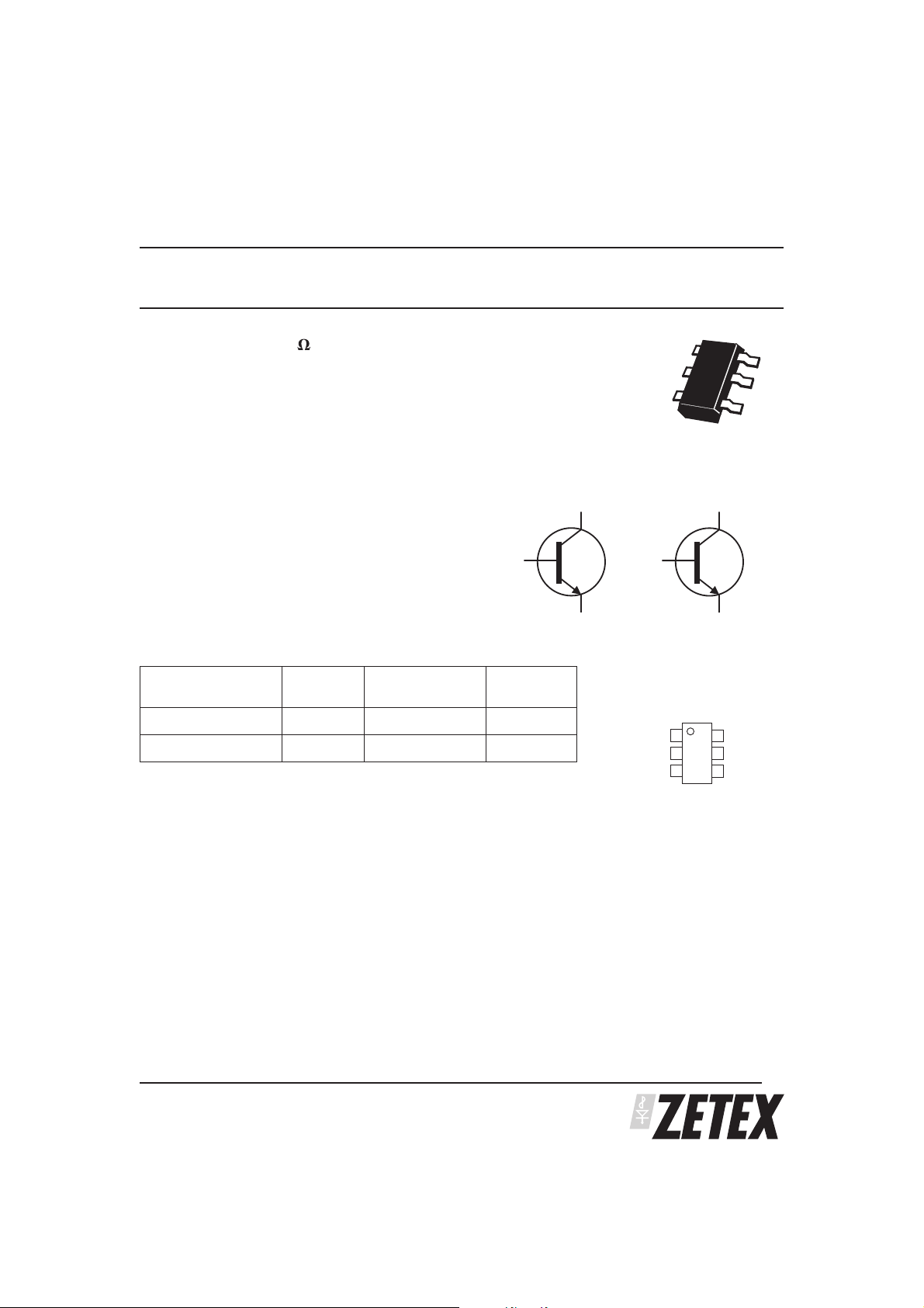
ZXTD09N50DE6E6
SuperSOT
DUAL 50V NPN SILICON LOW SATURATION SWITCHING TRANSISTOR
SUMMARY
V
=50V; R
CEO
DESCRIPTION
A dual NPN low saturation transistor combination contained in a single 6 lead
SOT23 package. Each transistor is the equivalent to the ZUMT619 device.
= 160m ;IC= 1A
SAT
FEATURES
Low Equivalent On Resistance
•
Low Saturation Voltage
•
I
=1A Continuous Collector Current
•
C
SOT23-6 package
•
APPLICATIONS
• LCD Backlighting inverter circuits
• Boost functions in DC-DC converters
•
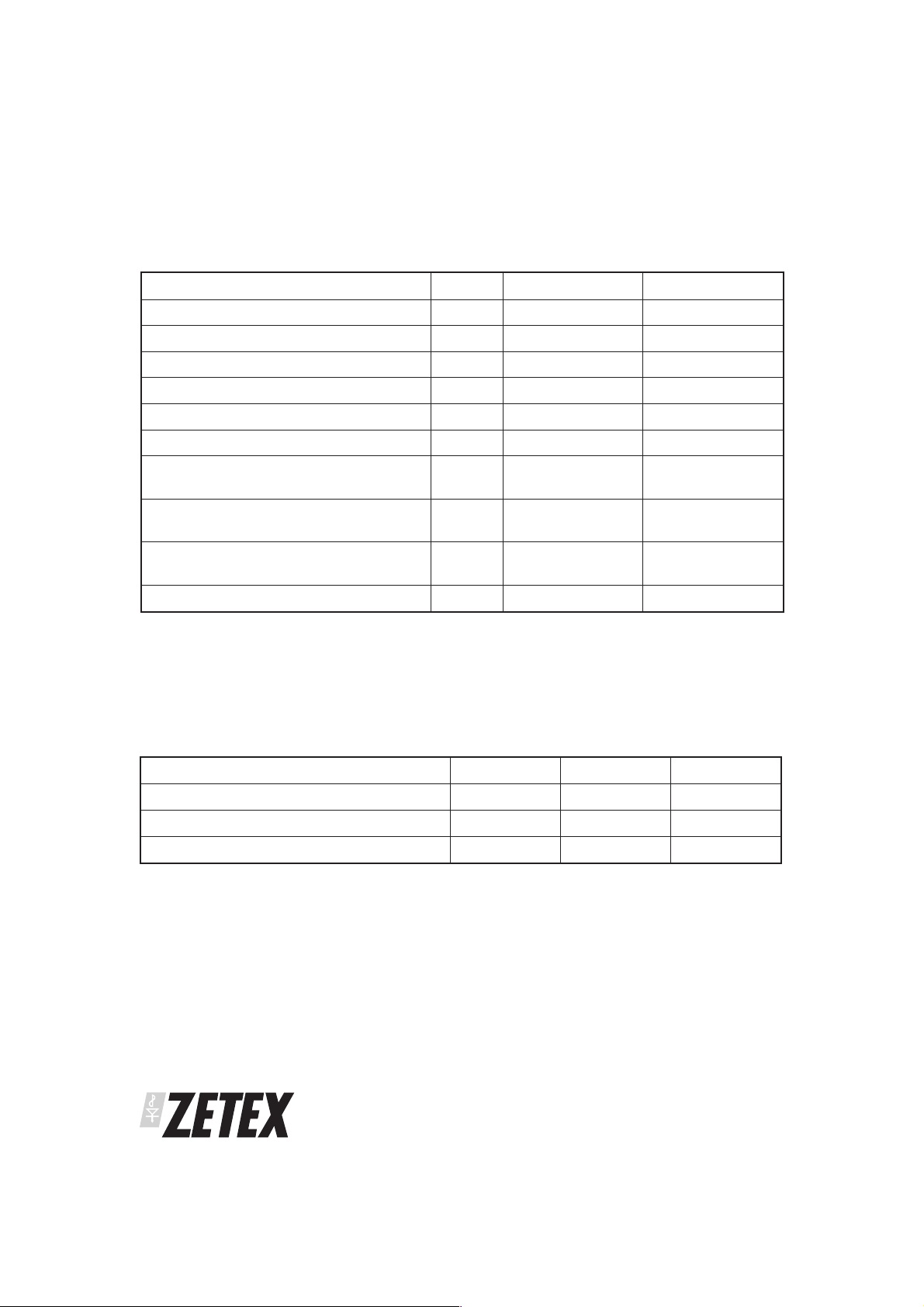
ORDERING INFORMATION
DEVICE REEL SIZE
ZXTD09N50DE6TA
ZXTD09N50DE6TC
DEVICE MARKING
D619
(inches)
7 8mm embossed 3000 units
13 8mm embossed 10000 units
TAPE WIDTH
(mm)
B1
QUANTITY
PER REEL
C1
E1
SOT23-6
B2
C1
E1
C2
Top View
C2
E2
B1
E2
B2
ISSUE 2 - JUNE 2001
1
Page 2
ZXTD09N50DE6
ABSOLUTE MAXIMUM RATINGS.
PARAMETER SYMBOL LIMIT UNIT
Collector-Base Voltage V
Collector-Emitter Voltage V
Emitter-Base Voltage V
Peak Pulse Current I
Continuous Collector Current I
Base Current I
Power Dissipation at TA=25°C (a)(d)
Linear Derating Factor
Power Dissipation at TA=25°C (a)(e)
Linear Derating Factor
Power Dissipation at TA=25°C (b)(d)
Linear Derating Factor
Operating and Storage Temperature Range T
CBO
CEO
EBO
CM
C
B
P
D
P
D
P
D
j:Tstg
50 V
50 V
5V
2A
1.0 A
200 mA
0.90
7.2
mW/°C
1.1
8.8
mW/°C
1.7
13.6
mW/°C
-55 to +150 °C
W
W
W
THERMAL RESISTANCE
PARAMETER SYMBOL VALUE UNIT
Junction to Ambient (a)(d) R
Junction to Ambient (b)(d) R
Junction to Ambient (a)(e) R
θJA
θJA
θJA
NOTES
(a) For a device surface mounted on 25mm x 25mm FR4 PCB with high coverage of single sided 1oz copper,
in still air conditions
(b) For a device surface mounted on FR4 PCB measured at t⭐5 secs.
(c) Repetitive rating - pulse width limited by maximum junction temperature. Refer to Transient Thermal
Impedance graph.
(d) For device with one active die.
(e) For device with two active die running at equal power.
2
139 °C/W
73 °C/W
113 °C/W
ISSUE 2 - JUNE 2001
Page 3
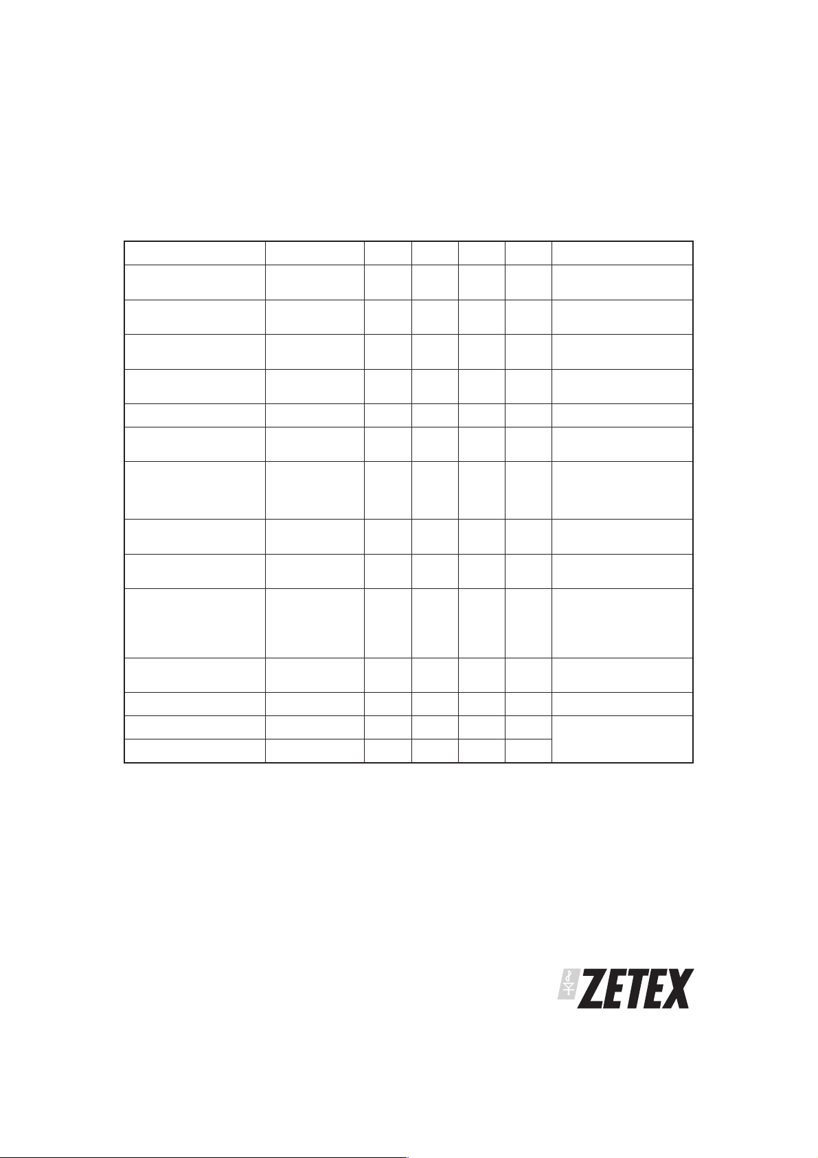
ZXTD09N50DE6E6
ELECTRICAL CHARACTERISTICS (at T
= 25°C unless otherwise stated).
amb
PARAMETER SYMBOL MIN. TYP. MAX. UNIT CONDITIONS.
Collector-Base
Breakdown Voltage
Collector-Emitter
Breakdown Voltage
Emitter-Base Breakdown
Voltage
Collector Cut-Off Current I
Emitter Cut-Off Current I
Collector Emitter Cut-Off
Current
Collector-Emitter
Saturation Voltage
Base-Emitter
Saturation Voltage
Base-Emitter Turn-On
Voltage
Static Forward Current
Transfer
Ratio
Transition
Frequency
Output Capacitance C
Turn-On Time t
Turn-Off Time t
V
(BR)CBO
V
(BR)CEO
V
(BR)EBO
CBO
EBO
I
CES
V
CE(sat)
V
BE(sat)
V
BE(on)
h
FE
f
T
obo
(on)
(off)
50 V
I
= 100µA
C
50 V IC= 10mA*
5V
I
= 100µA
E
10 nA VCB= 40V
10 nA VEB=4V
24
60
120
160
10 nA V
35
80
200
270
mV
mV
mV
mV
= 40V
CES
= 100mA, IB= 10mA*
I
C
= 250mA, IB= 10mA*
I
C
= 500mA, IB= 10mA*
I
C
= 1A, IB= 50mA*
I
C
940 1100 mV IC= 1A, IB= 50mA*
850 1100 mV IC= 1A, VCE=2V*
200
300
200
75
20
420
450
350
130
60
=10mA, VCE=2V*
I
C
= 100mA, VCE=2 V*
I
C
= 500mA, VCE=2V*
I
C
= 1A, VCE=2V*
I
C
= 1.5A, VCE=2 V*
I
C
215 MHz IC= 50mA, VCE=10V
f= 100MHz
10 pF VCB= 10V, f=1MHz
150 ns VCC=10V,IC=1A
=100mA
I
425 ns
B1=IB2
*Measured under pulsed conditions. Pulse width=300µs. Duty cycle ≤ 2%
ISSUE 2 - JUNE 2001
3
Page 4

ZXTD09N50DE6
TYPICAL CHARACTERISTICS
- (V)
CE(sat)
V
- Typical Gain
FE
h
800
600
400
200
1.15
0.4
+25°C
0.3
0.2
0.1
0
1m
IC/IB=10
IC/IB=50
IC/IB=100
10m 100m 1 10
IC- Collector Current (A)
V
CE(sat)
v I
C
VCE=2V
+100°C
+25°C
-55°C
0
10m 100m 1 10
1m
IC- Collector Current (A)
hFEv I
C
0.4
IC/IB=50
0.3
- (V)
0.2
CE(sat)
V
0.1
0
1m
-55°C
+25°C
+100°C
+150°C
10m 100m 1 10
IC- Collector Current (A)
V
CE(sat)
v I
C
1.0
IC/IB=50
0.8
0.6
- (V)
0.4
BE(sat)
V
0.2
0
10m 100m 1 10
1m
-55°C
+25°C
+100°C
+150°C
IC- Collector Current (A)
V
BE(sat)
v I
C
10
0.9
- (V)
0.6
BE(on)
V
0.3
0
10m 100m 1 10
1m
IC- Collector Current (A)
V
BE(on)
v I
-55°C
+25°C
+100°C
+150°C
C
1
DC
100m
- Collector Current (A)
C
I
10m
1s
100ms
10ms
1ms
100µs
100m 100
VCE- Collector Emitter Voltage (V)
110
Safe Operating Area
ISSUE 2 - JUNE 2001
4
Page 5

ZXTD09N50DE6E6
ISSUE 2 - JUNE 2001
5
Page 6

ZXTD09N50DE6
ISSUE 2 - JUNE 2001
6
Page 7

ZXTD09N50DE6E6
ISSUE 2 - JUNE 2001
7
Page 8

ZXTD09N50DE6
PACKAGE DIMENSIONS PAD LAYOUT DETAILS
e
b
2
L
E
e1
D
AA2
a
A1
DIM Millimetres Inches
Min Max Min Max
A 0.90 1.45 0.35 0.057
A1 0.00 0.15 0 0.006
A2 0.90 1.30 0.035 0.051
b 0.35 0.50 0.014 0.019
C 0.09 0.20 0.0035 0.008
D 2.80 3.00 0.110 0.118
E 2.60 3.00 0.102 0.118
E1 1.50 1.75 0.059 0.069
L 0.10 0.60 0.004 0.002
e 0.95 REF 0.037 REF
e1 1.90 REF 0.074 REF
L
0° 10° 0° 10°
E1
DATUM A
C
Zetex plc.
Fields New Road, Chadderton, Oldham, OL9-8NP, United Kingdom.
Telephone: (44)161 622 4422 (Sales), (44)161 622 4444 (General Enquiries)
Fax: (44)161 622 4420
Zetex GmbH Zetex Inc. Zetex (Asia) Ltd. These are supported by
Streitfeldstraße 19 Suite 315 3701-04 Metroplaza, Tower 1 agents and distributors in
D-81673 München 700 Veterans Memorial Highway Hing Fong Road, major countries world-wide
Germany Hauppauge NY11788 Kwai Fong Zetex plc 2001
Telefon: (49) 89 45 49 49 0 Telephone: (631) 543-7100 Telephone:(852) 26100 611
Fax: (49) 89 45 49 49 49 Fax: (631) 864-7630 Fax: (852) 24250 494 www.zetex.com
This publication is issued to provide outline information only which (unless agreed by the Company in writing) may not be used, applied or reproduced for
any purpose or form part of any order or contract or be regarded as a representation relating to the products or services concerned. The Company reserves
the right to alter without notice the specification, design, price or conditions of supply of any product or service.
USA Hong Kong
ISSUE 2 - JUNE 2001
8
 Loading...