

Page 1
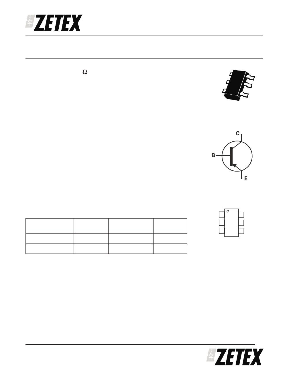
ZXT13P12DE6
C
C
SuperSOT4™
12V PNP SILICON LOW SATURATION SWITCHING TRANSISTOR
SUMMARY
V
=-12V; R
CEO
DESCRIPTION
This new 4th generation ultra low saturation transistor utilises the Zetex
matrix structure combined with advanced assembly techniques to give
extremely low on state losses. This makes it ideal for high efficiency, low
voltage switching applications.
FEATURES
Extremely Low Equivalent On Resistance
•
Extremely Low Saturation Voltage
•
characterised up to 15A
h
•
FE
I
=4A Continuous Collector Current
•
C
• SOT23-6 package
APPLICATIONS
• DC - DC Converters
• Power Management Functions
• Power switches
• Motor control
ORDERING INFORMATION
DEVICE REEL SIZE
ZXT13P12DE6TA 7 8mm embossed 3000 units
ZXT13P12DE6TC 13 8mm embossed 10000 units
= 37m ;IC= -4A
SAT
(inches)
TAPE WIDTH
(mm)
QUANTITY
PER REEL
SOT23-6
C
C
B
Top View
E
DEVICE MARKING
P12D
ISSUE 1 - DECEMBER 1999
1
Page 2
ZXT13P12DE6
ABSOLUTE MAXIMUM RATINGS.
PARAMETER SYMBOL LIMIT UNIT
Collector-Base Voltage V
Collector-Emitter Voltage V
Emitter-Base Voltage V
Peak Pulse Current I
Continuous Collector Current I
Base Current I
Power Dissipation at TA=25°C (a)
Linear Derating Factor
Power Dissipation at TA=25°C (b)
Linear Derating Factor
Operating and Storage Temperature Range T
CBO
CEO
EBO
CM
C
B
P
D
P
D
j:Tstg
-20 V
-12 V
-7.5 V
-15 A
-4 A
-500 mA
1.1
8.8
mW/°C
1.7
13.6
mW/°C
-55 to +150 °C
W
W
THERMAL RESISTANCE
PARAMETER SYMBOL VALUE UNIT
Junction to Ambient (a) R
Junction to Ambient (b) R
θJA
θJA
NOTES
(a) For a device surface mounted on 25mm x 25mm FR4 PCB with high coverage of single sided 1oz copper,
in still air conditions
(b) For a device surface mounted on FR4 PCB measured at t⭐5 secs.
ISSUE 1 - DECEMBER 1999
2
113 °C/W
73 °C/W
Page 3

TYPICAL CHARACTERISTICS
10
DC
1
1s
100ms
10ms
100m
Collector Current (A)
C
Single Pulse Tamb=25°C
I
10m
100m 1 10
VCECollector-Emitter Voltage (V)
120
)
100
(°C/W
80
D=0.5
60
1ms
100µs
Safe Operating Area
ZXT13P12DE6
1.2
)
1.0
(W
0.8
0.6
0.4
er Dissipation
Pow
0.2
ax
M
0.0
0 20 40 60 80 100 120 140 160
Temperature (°C)
Derating Curve
40
D=0.2
al Resistance
20
0
Therm
100µ 1m 10m 100m 1 10 100 1k
D=0.1
Single Pulse
D=0.05
Pulse Width (s)
Transient Thermal Impedance
ISSUE 1 - DECEMBER 1999
3
Page 4

ZXT13P12DE6
ELECTRICAL CHARACTERISTICS (at T
= 25°C unless otherwise stated).
amb
PARAMETER SYMBOL MIN. TYP. MAX. UNIT CONDITIONS.
Collector-Base Breakdown
Voltage
Collector-Emitter Breakdown
Voltage
Emitter-Base Breakdown Voltage V
Collector Cut-Off Current I
Emitter Cut-Off Current I
Collector Emitter Cut-Off Current I
Collector-Emitter Saturation
Voltage
Base-Emitter Saturation Voltage V
Base-Emitter Turn-On Voltage V
Static Forward Current Transfer
Ratio
Transition Frequency f
Output Capacitance C
Turn-On Time t
Turn-Off Time t
V
(BR)CBO
V
(BR)CEO
(BR)EBO
CBO
EBO
CES
V
CE(sat)
BE(sat)
BE(on)
h
FE
T
obo
(on)
(off)
-20 -33 V IC=-100A
-12 -25 V IC=-10mA*
-7.5 -8.5 V IE=-100A
-100 nA VCB=-16V
-100 nA VEB=-6V
-100 nA V
-7.5
-10
-68
-135
-200
-150
-90
-175
-250
-175
mV
mV
mV
mV
mV
=-16V
CES
=-0.1A, IB=-10mA*
I
C
=-1A, IB=-10mA*
I
C
=-3A, IB=-50mA*
I
C
=-4A, IB=-50mA*
I
C
=-4A, IB=-400mA*
I
C
-1.0 V IC=-4A, IB=-50mA*
-0.9 V IC=-4A, VCE=-2V*
300
300
200
20
500
450
300
30
900
=-10mA, VCE=-2V*
I
C
=-1A, VCE=-2V*
I
C
=-4A, VCE=-2V*
I
C
=-15A, VCE=-2V*
I
C
55 MHz IC=-50mA, VCE=-10V
f=50MHz
115 pF VCB=-10V, f=1MHz
70 ns VCC=-10V, IC=-3A
=-60mA
I
265 ns
B1=IB2
*Measured under pulsed conditions. Pulse width=300µs. Duty cycle 2%
ISSUE 1 - DECEMBER 1999
4
Page 5

100m
Tamb=25°C
ZXT13P12DE6
TYPICAL CHARACTERISTICS
0.25
IC/IB=50
0.20
(V)
CE(SAT)
V
IC/IB=100
10m
IC/IB=50
1m
1m 10m 100m 1 10
IC/IB=10
ICCollector Current (A)
V
CE(SAT)vIC
1.6
1.4
100°C
1.2
ain
G
1.0
0.8
alised
0.6
0.4
orm
N
0.2
0.0
1m 10m 100m 1 10
25°C
-55°C
ICCollector Current (A)
hFEvI
C
VCE=2V
0.15
(V)
0.10
CE(SAT)
V
0.05
0.00
1m 10m 100m 1 10
100°C
25°C
ICCollector Current (A)
V
CE(SAT)vIC
IC/IB=50
1.0
0.8
(V)
0.6
BE(SAT)
V
0.4
1m 10m 100m 1 10
-55°C
25°C
100°C
ICCollector Current (A)
V
BE(SAT)vIC
-55°C
VCE=2V
1.0
(V)
)
N
BE(O
V
0.8
0.6
0.4
-55°C
25°C
100°C
1m 10m 100m 1 10
ICCollector Current (A)
V
BE(ON)vIC
ISSUE 1 - DECEMBER 1999
5
Page 6

ZXT13P12DE6
PACKAGE DIMENSIONS PAD LAYOUT DETAILS
e
b
2
L
E
e1
D
AA2
a
A1
DIM Millimetres Inches
Min Max Min Max
A 0.90 1.45 0.35 0.057
A1 0.00 0.15 0 0.006
A2 0.90 1.30 0.035 0.051
b 0.35 0.50 0.014 0.019
C 0.09 0.20 0.0035 0.008
D 2.80 3.00 0.110 0.118
E 2.60 3.00 0.102 0.118
E1 1.50 1.75 0.059 0.069
L 0.10 0.60 0.004 0.002
e 0.95 REF 0.037 REF
e1 1.90 REF 0.074 REF
L
0° 10° 0° 10°
E1
DATUM A
C
Zetex plc.
Fields New Road, Chadderton, Oldham, OL9-8NP, United Kingdom.
Telephone: (44)161 622 4422 (Sales), (44)161 622 4444 (General Enquiries)
Fax: (44)161 622 4420
Zetex GmbH Zetex Inc. Zetex (Asia) Ltd. These are supported by
Streitfeldstraße 19 47 Mall Drive, Unit 4 3510 Metroplaza, Tower 2 agents and distributors in
D-81673 München Commack NY 11725 Hing Fong Road, major countries world-wide
Germany USA Kwai Fong, Hong Kong © Zetex plc 1999
Telefon: (49) 89 45 49 49 0 Telephone: (631) 543-7100 Telephone:(852) 26100 611
Fax: (49) 89 45 49 49 49 Fax: (631) 864-7630 Fax: (852) 24250 494 Internet:http://www.zetex.com
This publication is issued to provide outline information only which (unless agreed by the Company in writing) may not be used, applied or reproduced for
any purpose or form part of any order or contract or be regarded as a representation relating to the products or services concerned. The Company reserves
the right to alter without notice the specification, design, price or conditions of supply of any product or service.
ISSUE 1 - DECEMBER 1999
6
 Loading...