

Page 1
LED DRIVER SOLUTION FOR LCD BACKLIGHTING
DEVICE DESCRIPTION
ZXSC310
The ZXSC310 is a single or multi cell LED driver
designed for LCD backlighting applications. The input
voltage range of the device is between 0.8V and 8V.
This means the ZXSC310 is compatible with single
NiMH, NiCd or Alkaline cells, as well as multi-cell or
LiIon batteries.
The device features a shutdowncontrol, resulting in a
standby current less than 5µA, and an output capable
of driving serial or parallel LED’s. The circuit generates
constant power output, which are ideal for driving
singleormultipleLED’soverawiderangeofoperating
voltages. These features make the device ideal for
drivingLED’sparticularlyinLCDbacklightapplications
for Digital Still cameras and PDA’s.
FEATURES
· 94% efficiency
· Minimum operating input voltage 0.8V
· Maximum operating input voltage 8V
· Standby current less than 5µA
· Programmable output current
· Series or parallel LED configuration
· Low saturation voltage switching transistor
·
SOT23-5 package
APPLICATIONS
·
LCD backlights:
Digital still camera
PDA
Mobile phone
·
LED flashlights and torches
·
White LED driving
·
Multiple LED driving
ORDERING INFORMATION
DEVICE REEL
SIZE
ZXSC310E5TA 180mm 8mm 3000
TAPE
WIDTH
QUANTITY
PER REEL
The ZXSC310 is a PFM DC-DC controller IC that drives
an external Zetex switching transistor with a very low
saturation resistance. These transistors are the best
switching devices available for this type of conversion
enabling high efficiency conversion with low input
voltages. The drive output of the ZXSC310 LED driver
generates a dynamic drive signal for the switching
transistor.
The circuit can start up under full load and operates
down to an input voltage of 0.8 volts. The solution
configurationensuresoptimumefficiencyoverawider
range of load currents; several circuit configurations
are possible depending on battery life versus
brightness considerations.
TheZXSC310is offered in the SOT23-5 package which,
when combined with a SOT23 switching transistor,
generates a high efficiency small size circuit solution.
The IC and discrete combination offers the ultimate
cost Vs performance solution for LED backlight
applications.
TYPICAL APPLICATIONS CIRCUIT
V
=3.3V/5V
IN
V
CC
V
DRIVE
S
TDN
I
SENSE
GND
DEVICE MARKINGS
·
C310
Package SOT23-5
ISSUE 2 - MARCH 2004
1
SEMICONDUCTORS
Page 2
ZXSC310
ABSOLUTE MAXIMUM RATINGS:
Supply Voltage -0.3 to 10V
Maximum Voltage other pins -0.3 to V
Power Dissipation 450mW
Operating Temperature -40 to 85 °C
Storage Temperature -55 to 150°C
ELECTRICAL CHARACTERISTICS:
Test conditions unless otherwise stated: V
Symbol Parameter Conditions Min Typ Max Units
Efficiency
V
CC
V
CC(min)
I
Q
I
VDRIVE
I
CC
Recommended supply
voltage range
Minimum startup and
operating voltage
Quiescent current
Base drive current V
Supply current
1
2
3
CC
I
=-600µA,V
DRIVE
=-600µA, V
I
DRIVE
T
=-10°C3
AMB
V
EN =VCC
0V (standby)
V
EN =
DRIVE
V
DRIVE
=1.5V, T
(enabled)
= 0.7V, V
= 0.7V, V
+0.3V
CC
=25 C
AMB
0.8 8 V
DRIVE
DRIVE
=0.7V
=0.7V,
0.8
0.9
0.2
510mAµA
= 0V 1.5 3.5 mA
ISENSE
=0V 2 4 mA
ISENSE
94 %
0.92 V
V
VDRIVE(high)
V
VDRIVE(low)
V
STDN(high)
V
STDN(low)
I
STDN
V
ISENSE
(threshold)
T
CVISENSE
I
ISENSE
T
DRV
High level drive voltage V
Low level drive voltage V
ISENSE
ISENSE
=0V,I
VDRIVE
= 50mV, I
=-0.5mA V
= 5mA 0 0.2 V
VDRIVE
Device enabled 0.7 V
Device in standby mode 0.15 V
Enable input current -1 1 µA
Output current reference
voltage
I
voltage temp co.
SENSE
I
input current V
SENSE
2
= 0V 0 -30 -65 µA
ISENSE
Discharge Pulse Width 1.2 1.7 3.2 µs
OPERATING CONDITIONS
Symbol
F
OSC
1 Application dependent, see reference designs
2 These parameters guaranteed by Design and characteristics
3 Total supply current =I
4 Operating frequency is application circuit dependent. See applications section.
Parameter Conditions Min Typ Max Units
Recommended operating
frequency
Q+IVDRIVE
4
, see typical characteristics
CC
V
CC
-0.3
14 19 24 mV
0.4 %/°C
200 kHz
ISSUE 2 - MARCH 2004
V
SEMICONDUCTORS
2
Page 3
ZXSC310
FMMT618
For the circuits described in the applications section
ZetexFMMT618 isthe recommendedpass transistor.
ELECTRICAL CHARACTERISTICS:
Test conditions unless otherwise stated: T
Symbol Parameter Conditions Min Typ Max Units
V
CE(sat)
V
(BR)CEO
5
Measured under pulse conditions. Pulse width=300µs. Duty cycle ⱕ2%
Collector-Emitter
Saturation Voltage
Collector-Emitter
Breakdown Voltage
5
5
IC=0.1A, IB=10mA
I
C
I
C
IC=10mA 20 27 V
ZHCS1000
The following indicates outline data for the device,
more detailed information can be found in the Zetex
surface mount products data book or on Zetex Web
page: www.zetex.com
=25 C
AMB
8
=1A, IB=10mA
=2.5A, IB=50mA
70
130
15
150
200
mV
For the maximum brightness circuit described in the
applications section Zetex ZHCS1000 is the
recommended Schottky diode.
The following indicates outline data for the ZHCS,
more detailed information can be found on Zetex Web
page: www.zetex.com
ELECTRICAL CHARACTERISTICS:
Test conditions unless otherwise stated: T
Symbol Parameter Conditions Min Typ Max Units
V
F
t
rr
I
R
Part
Number
BAT54 30 200 0.6 500 30 250 25 10 SOT23-6
ZHCS2000 40 2000 20 500 2000 1000 30 60 SOT23
ZHCS1000 40 1000 12 500 1000 100 30 25 SOT23
ZHCS750 40 750 12 540 750 100 30 25 SOT23
ZHCS500 40 500 6.75 550 500 40 30 20 SOT23
ZHCS400 40 400 6.75 500 400 40 30 20 SOT323
Forward voltage IF= 500mA
I
F
Reverse Recovery Time Switched from IF=500mA to
I
R
Measured at I
Reverse Current VR= 30V 50 100 µA
V
I
R
I
F
FSM
VFat IRat Capacitance
Max.VMax.mAMax.AMax.mVI
mA
AMB
=1A
=500mA.
Max.AV
F
=25 C
=50mA
R
R
V
= 25V, f = 1MHz
at V
R
Typ.
pF
400
500
12 ns
Package
SOT23
mV
ISSUE 2 - MARCH 2004
3
SEMICONDUCTORS
Page 4
ZXSC310
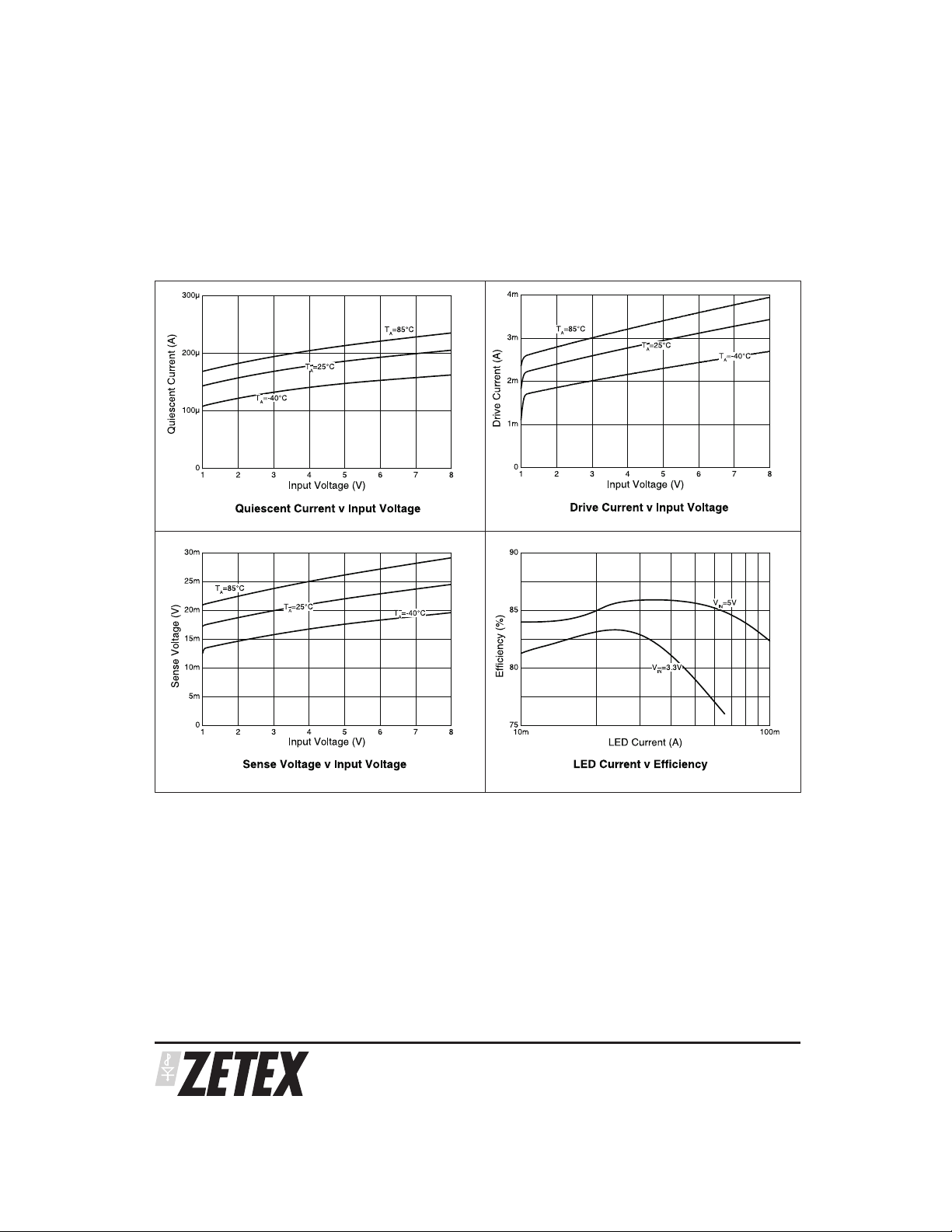
TYPICAL CHARACTERISTICS
SEMICONDUCTORS
ISSUE 2 - MARCH 2004
4
Page 5
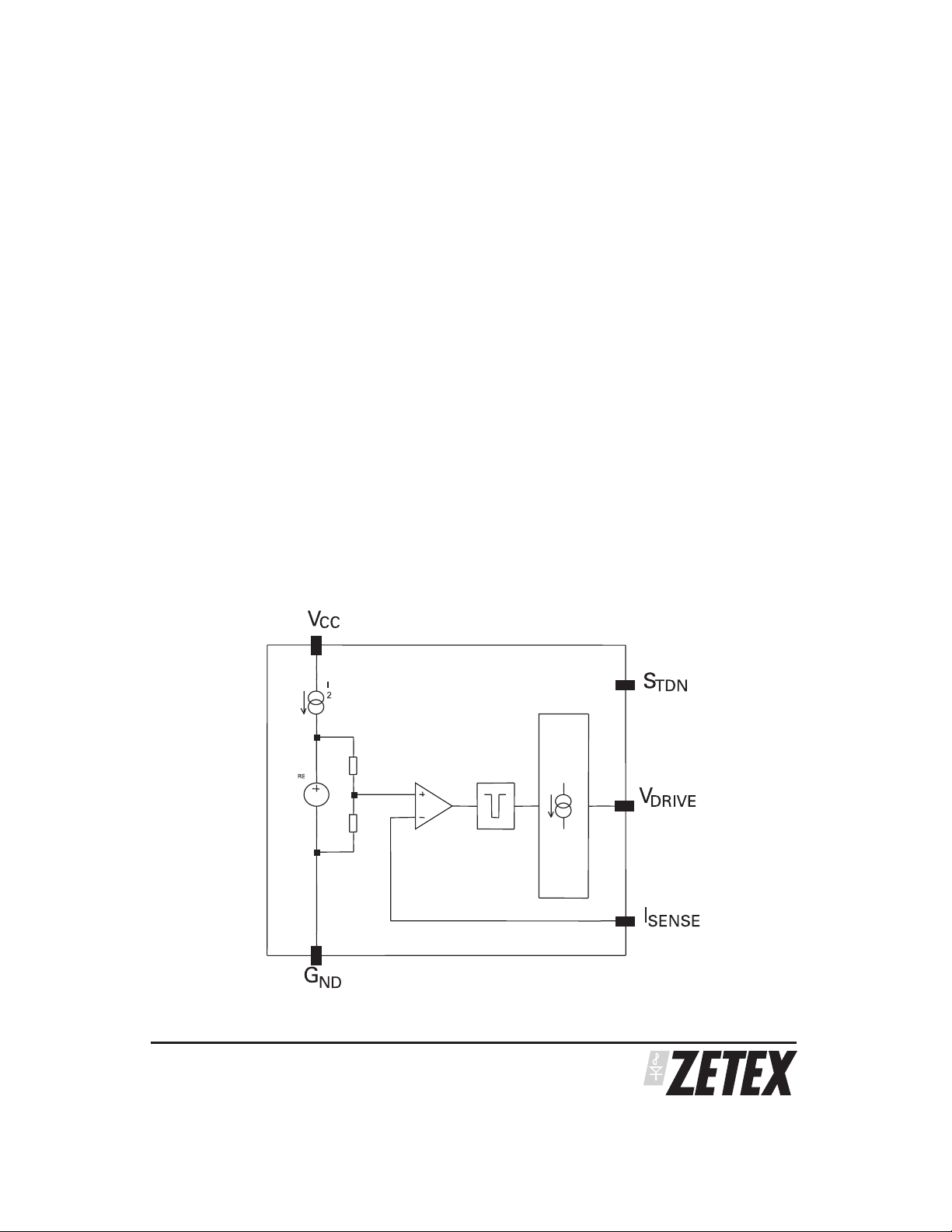
DEVICE DESCRIPTION
ZXSC310
The ZXSC310 is PFM, controller IC which, when
combinedwith a high performance external transistor,
enables the production of a high efficiency boost
converter for LED driving applications. A block
diagram is shown for the ZXSC310 below.
The on chip comparator forces the driver circuit and
therefore the external switching transistor off if the
voltage at I
circuit and divider set this threshold.
The voltage at I
resistor connected in series with the emitter of the
switching transistor. A monostable following the
outputofthecomparatorforcestheturn-offtimeofthe
output stage to be typically 1.7us. This ensures that
there is sufficient time to discharge the inductor coil
before the next on period.
exceeds 19mV. An internal reference
SENSE
is taken from a current sense
SENSE
With every on pulse the switching transistor is kept on
until the voltage across the current-sense resistor
exceeds the threshold of the I
length, and therefore the switching frequency, is
determinedby theprogrammed peak current,the input
voltageand the inputto output voltagedifferential. See
applications section for details.
The driver circuit supplies the external switching
transistor with a fixed drive current. To maximise
efficiency the external transistor switched quickly,
typically being forced off within 30ns.
Drive
input. The on-pulse
SENSE
ZXSC310 Block Diagram
ISSUE 2 - MARCH 2004
R1
V
R2
5
I
SEMICONDUCTORS
Page 6

ZXSC310
REFERENCE DESIGNS
Three typical LED driving applications are shown.
Firstly a typical LCD backlight circuit, then maximum
brightness LED driving solution and lastly an
optimised battery life LED driving solution.
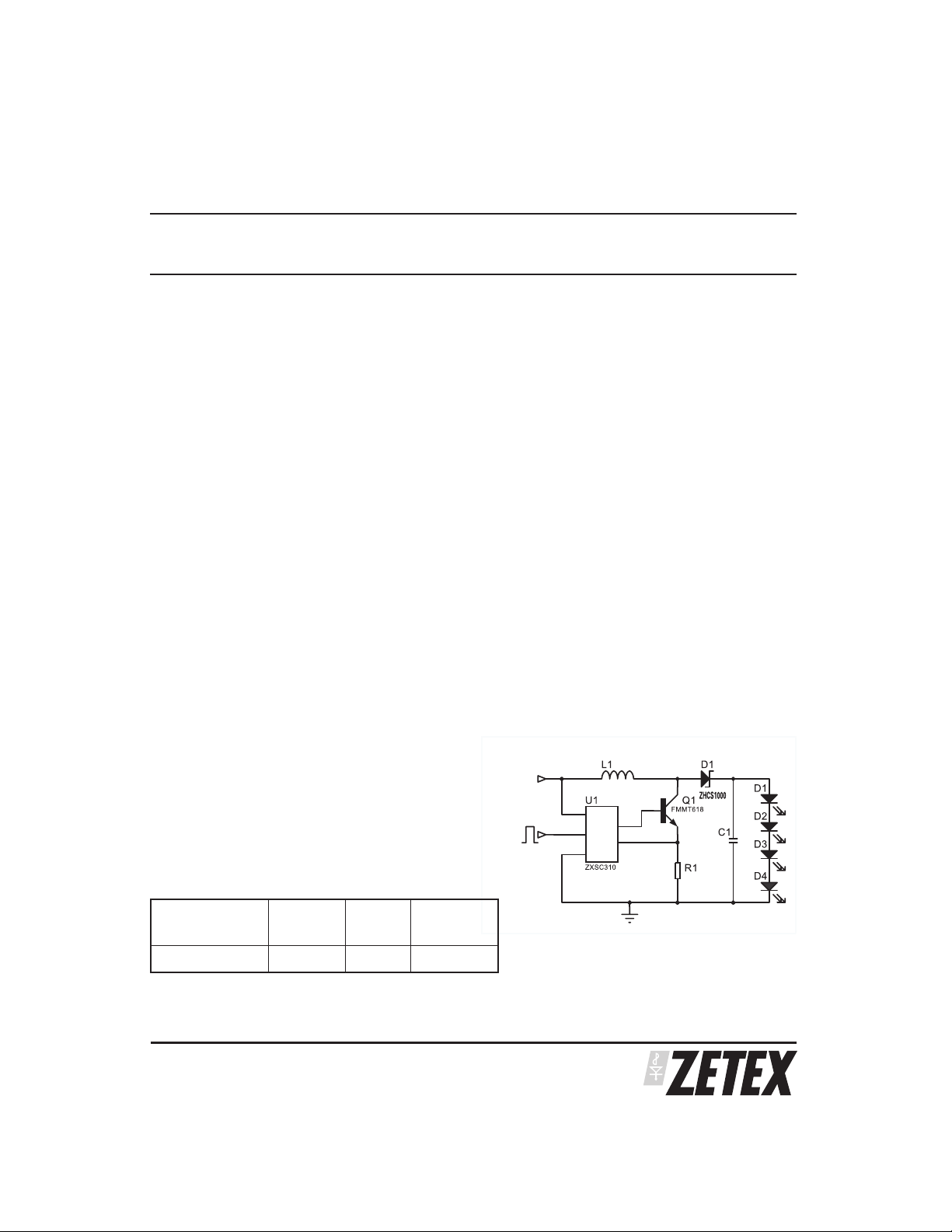
LCD backlight circuit
= 3.3V / 5V
This application shows the ZXSC310 in a typical LCD
backlight application for Digital Still Cameras and
PDA’s.The input voltageforthese backlight circuits are
usually fixed from the main system power, typically
3.3V or 5V. The LED’s are connected serially so that the
light is distributed uniformly in each LED. The current
provided to the LED’s can either be pulsed or DC. The
DC current is programmable via a sense resistor,
R
, and is set to an optimum LED current of 20mA
SENSE
for the reference designs. DC current is achieved by
adding a Schottky rectifying diode and an output
capacitor, as shown in the reference design below.
(Notes)
Materials list
Ref Value Part Number Manufacture Comments
U1 N/A ZXSC310E5 Zetex Plc Single cell converter, SOT23-5
Q1 N/A FMMT618 Zetex Plc Low V
D1 N/A ZHCS1000 Zetex Plc 1A Schottky diode, SOT23
C1 2.2F Generic Various 0805 Size
6
R1
7
R1
8
L1
6
Used for 3.3V input, I
7
Used for 5V input, I
8
See Application section.
SEMICONDUCTORS
150m⍀ Generic Various 1206 Size
250m⍀
68µH Surface mount inductor
set to 20mA ⫾10%.
LED
to 20mA ⫾10%.
LED
Generic Various 1206 Size
6
) NPN, SOT23
CE(sat
ISSUE 2 - MARCH 2004
Page 7

ZXSC310
Maximum brightness solution
This circuit provides a continuous current output to the
LED by rectifying and buffering the DC-DC output. This
ensures maximum LED brightness.
(Notes)
Materials list
Ref Value Part Number Manufacturer Comments
U1 N/A ZXSC310E5 Zetex Plc Single cell converter, SOT23-5
Q1 N/A FMMT617 Zetex Plc Low
D1 1A ZHCS1000 Zetex Plc 1A Shottky diode, SOT23
R1 100m⍀ Generic Various 0805 Size
C1 2.2 F
L1 100µH
8
See Application section.
ISSUE 2 - MARCH 2004
8
Generic Various Low ESR ceramic capacitor
Surface mount inductor
7
NPN, SOT23
VCE(sat)
SEMICONDUCTORS
Page 8

ZXSC310
Maximum battery life solution
To ensure optimum efficiency, and therefore
maximum battery life, the LED is supplied with a
pulsed current. Maximum efficiency is ensured with
the removal of rectifier losses experienced in the
maximum brightness solution.
(Notes)
Materials list
Ref Value Part
U1 N/A ZXSC310E5 Zetex Plc Single cell converter, SOT23-5
Q1 N/A FMMT617 Zetex Plc Low V
R1 330m⍀ Generic Various 0805 Size
L1 100H
8
See Application section.
SEMICONDUCTORS
8
Number
Manufacturer Comments
NPN, SOT23
CE(SAT)
Surface mount inductor
ISSUE 2 - MARCH 2004
8
Page 9

APPLICATIONS INFORMATION
ZXSC310
The following section is a design guide for optimum
converter performance.
Switching transistor selection
The choice of switching transistor has a major impact
onthe converter efficiency. For optimumperformance,
a bipolar transistor with low V
required.
The Zetex FMMT618 is an ideal choice of transistor,
having a low saturation voltage. A data sheet for the
FMMT618 is available on Zetex web site or through
your local Zetex sales office. Outline information is
included in the characteristics section of this data
sheet.
0.4
0.
3
0.2
1
0.
0
0.
and high gain is
CE(SAT)
Schottky diode selection
For the maximum battery life solution a Schottky
rectifier diode is not required. As with the switching
transistor the Schottky rectifier diode has a major
impact on the converter efficiency. A Schottky diode
with a low forward voltage and fast recovery time
should be used for this application.
The diode should be selected so that the maximum
forward current is greater or equal to the maximum
peakcurrent in the inductor, and the maximumreverse
voltage is greater or equal to the output voltage.
The Zetex ZHCS1000 meets these needs. Datasheets
for the ZHCS Series are available on Zetex web site or
through your local Zetex sales office. Outline
information is included in the characteristics section of
this data sheet.
For the maximum brightness solution a pulsed current
is supplied to the LED and thus a Schottky rectifier
diode is required.
Inductor selection
The inductor value must be chosen to satisfy
performance, cost and size requirements of the overall
solution. For the LCD backlight reference design we
recommend an inductor value of 68uH with a core
saturation current rating greater than the converter
peak current value and low series resistance.
Inductor selection has a significant impact on the
converter performance. For applications where
efficiencyis critical,aninductor with aseries resistance
of 500m⍀ or less should be used.
A list of recommended inductors is shown in the table
below:
Part No. Manufacture L I
DO1608C-683 Coilcraft 68H 0.4A 0.86⍀
CR54-680 Sumida 68H 0.61A 0.46⍀
P1174.683 Pulse 68H 0.4A 0.37⍀
SFOP5845-R61680 Samwha 68H 0.61A 0.46⍀
SIS43-680 Delta 68 H 0.4 1.125⍀
PK
R
DC
ISSUE 2 - MARCH 2004
9
SEMICONDUCTORS
Page 10

ZXSC310
Peak current definition
The peak current rating is a design parameter whose
value is dependent upon the overall application. For
the high brightness reference designs, a peak current
of was chosen to ensure that the converter could
provide the required output power to the LED.
In general, the I
value must be chosen to ensure that
PK
the switching transistor, Q1, is in full saturation with
maximum output power conditions, assuming
worse-case input voltage and transistor gain under all
operating temperature extremes.
Input Voltage
(V)
3.3V 10 3 510 68 80
3.3V 10 4 330 68 81
3.3V 10 6 150 68 79
3.3V 20 3 220 68 84
3.3V 20 4 150 68 93
3.3V 20 6 77 68 79
3.3V 30 3 170 68 84
3.3V 30 4 100 68 84
3.3V 30 6 47 68 77
5V 10 3 750 68 83
5V 10 4 510 68 84
5V 10 6 330 68 79
5V 20 3 440 68 85
5V 20 4 250 68 85
5V 20 6 150 68 82
5V 30 3 330 68 86
5V 30 4 170 68 85
5V 30 6 100 68 83
LED current
(mA)
No. of LED’s R
Once I
is decided the value of R
PK
SENSE
can be
determined by:
ISENSE
V
R
SENSE
=
I
PK
A selection guide of sense resistor and inductor values
for given input voltages, output currents and number
of LED connected in series is provided in the table
below.
SENSE
(m )
Inductor
( H)
Efficiency
(%)
SEMICONDUCTORS
ISSUE 2 - MARCH 2004
10
Page 11

ZXSC310
Output Power Calculation
By making the above assumptions for inductance and
peak current the outputpowercan bedetermined by:
OFF
PVVI
OUT OUT IN AV
=−××
()
Note:V
drop.
=output voltage + Schottky rectifier voltage
OUT
Where
1.7us (internally set by ZXSC310)
T
≅
OFF
and
()
OFF OUT IN
TV V
T
ON
=
−
V
IN
and
PK MIN
II
+
I
AV
=
2
T
TT
+
ON OFF
Capacitor selection
For pulsed operation, as in the maximum battery life
solution,no capacitors are required at the output to the
LED. For rectified operation, as in the maximum
brightness solution, a small value ceramic capacitor is
required, typically 2.2uF.
Generallyan inputcapacitoris not required,but a small
ceramic capacitor may be added to aid EMC, typically
470nF to 1uF.
(notes)
Where
()
OUT IN OFF
VVT
II
MIN PK
=−
−×
L
Operating frequency can be derived by:
F
1
=
()
ON OFF
TT
+
ISSUE 2 - MARCH 2004
11
SEMICONDUCTORS
Page 12

ZXSC310
Shutdown Control
The ZXSC310 offers a shutdown mode that produces a
standby current of less than 5uA when in operation.
When the voltage at the S
ZXSC310 is enabled, hence the driver is in normal
operation. When the voltage at the S
lower the ZXSC310 is disabled, hence the driver is in
shutdown mode. If the S
ZXSC310 is also enabled.
pin is 0.7V or higher the
TDN
pin is 0.1V or
TDN
pin is open circuit the
TDN
Demonstration board
A demonstration board for the LCD backlighting
solution, is available upon request. These can be
obtained through your local Zetex office or through
Zetexwebpages. For all reference designs Gerber files
and bill of materials can be supplied.
Layout of LCD backlighting solution
Top Silk Drill File
Top Copper Bottom Copper
SEMICONDUCTORS
ISSUE 2 - MARCH 2004
12
Page 13

PINOUT DIAGRAM
ZXSC310
VCC
Gnd
STDN
1
5
2
3
4
Top View
PIN DESCRIPTIONS
Pin No. Name Description
1V
2G
3S
4I
5V
CC
nd
TDN
SENSE
DRIVE
Supply voltage, generally Alkaline, NiMH or NiCd single cell
Ground
Shutdown
Inductor current sense input. Internal threshold voltage set to 19mV.
Connect external sense resistor
Drive output for external switching transistor. Connect to base of
external switching transistor.
VDRIVE
ISENSE
ISSUE 2 - MARCH 2004
13
SEMICONDUCTORS
Page 14

ZXSC310
(NOTES)
SEMICONDUCTORS
ISSUE 2 - MARCH 2004
14
Page 15

(NOTES)
ZXSC310
ISSUE 2 - MARCH 2004
15
SEMICONDUCTORS
Page 16

ZXSC310
SOT23-5 PACKAGE DIMENSIONSSOT23-5 PACKAGE OUTLINE
DIM Millimeters Inches
MIN MAX MIN MAX
A 0.90 1.45 0.035 0.057
A1 0.00 0.15 0.00 0.006
A2 0.90 1.3 0.035 0.051
b 0.35 0.50 0.014 0.020
C 0.09 0.20 0.0035 0.008
D 2.80 3.00 0.110 0.118
E 2.60 3.00 0.102 0.118
E1 1.50 1.75 0.059 0.069
e 0.95 REF 0.037 REF
e1 1.90 REF 0.075 REF
L 0.10 0.60 0.004 0.024
a° 0 10 0 10
© Zetex plc 2004
Europe
Zetex GmbH
Streitfeldstraße 19
D-81673 München
Germany
Telefon: (49) 89 45 49 49 0
Fax: (49) 89 45 49 49 49
europe.sales@zetex.com
These offices are supported by agents and distributors in major countries world-wide.
Thispublicationis issued to provideoutline information only which(unless agreed by theCompany in writing) maynotbe used, applied orreproduced
for any purpose or form part of any order or contract or be regarded as a representation relating to the products or services concerned. The Company
reserves the right to alter without notice the specification, design, price or conditions of supply of any product or service.
For the latest product information, log on to www.zetex.com
Americas
Zetex Inc
700 Veterans Memorial Hwy
Hauppauge, NY 11788
USA
Telephone: (1) 631 360 2222
Fax: (1) 631 360 8222
usa.sales@zetex.com
Asia Pacific
Zetex (Asia) Ltd
3701-04 Metroplaza Tower 1
Hing Fong Road, Kwai Fong
Hong Kong
Telephone: (852) 26100 611
Fax: (852) 24250 494
asia.sales@zetex.com
Corporate Headquaters
Zetex plc
Fields New Road, Chadderton
Oldham, OL9 8NP
United Kingdom
Telephone (44) 161 622 4444
Fax: (44) 161 622 4446
hq@zetex.com
ISSUE 2 - MARCH 2004
SEMICONDUCTORS
16
SCZXSC310DS1
 Loading...