

Page 1
SINGLE OR MULTI CELL LED DRIVER SOLUTION
DESCRIPTION
The ZXSC300 is a single or multi cell LED driver
designed for applications where step-up voltage
conversion from very low input voltages is required.
Theseapplicationsmainlyoperatefromsingle1.5Vor
1.2V battery cells. The circuit generates constant
current pulses that are ideal for driving single or
multiple LED’s over a wide range of operating
voltages.
The ZXSC300 is a PFM controller IC that drives an
external Zetex switching transistor with a very low
saturation resistance. These transistors are the best
switching devices available for this type of switching
conversion enabling high efficiency conversion with
input voltages below 1 volt. The drive output of the
ZXSC controller generates a dynamic drive signal for
FEATURES
• 94% efficiency
• Minimum operating input voltage 0.8V
• Fixed output current
• Low saturation voltage switching transistor
•
SOT23-5 package
the switching transistor.
The circuit can start up under full load and operates
down to an input voltage of 0.8 volts. The solution
configurationensuresoptimumefficiencyovera wide
range of load currents, several circuit configurations
are possible depending on battery life versus
brightness considerations.
The ZXSC300 is offered in the SOT23-5 package
which, when combined with a SOT23 switching
transistor, generates a high efficiency small size
circuit solution. The IC and discrete combination
offers the ultimate cost vs performance solution for
single cell LED driving applications.
ZXSC300
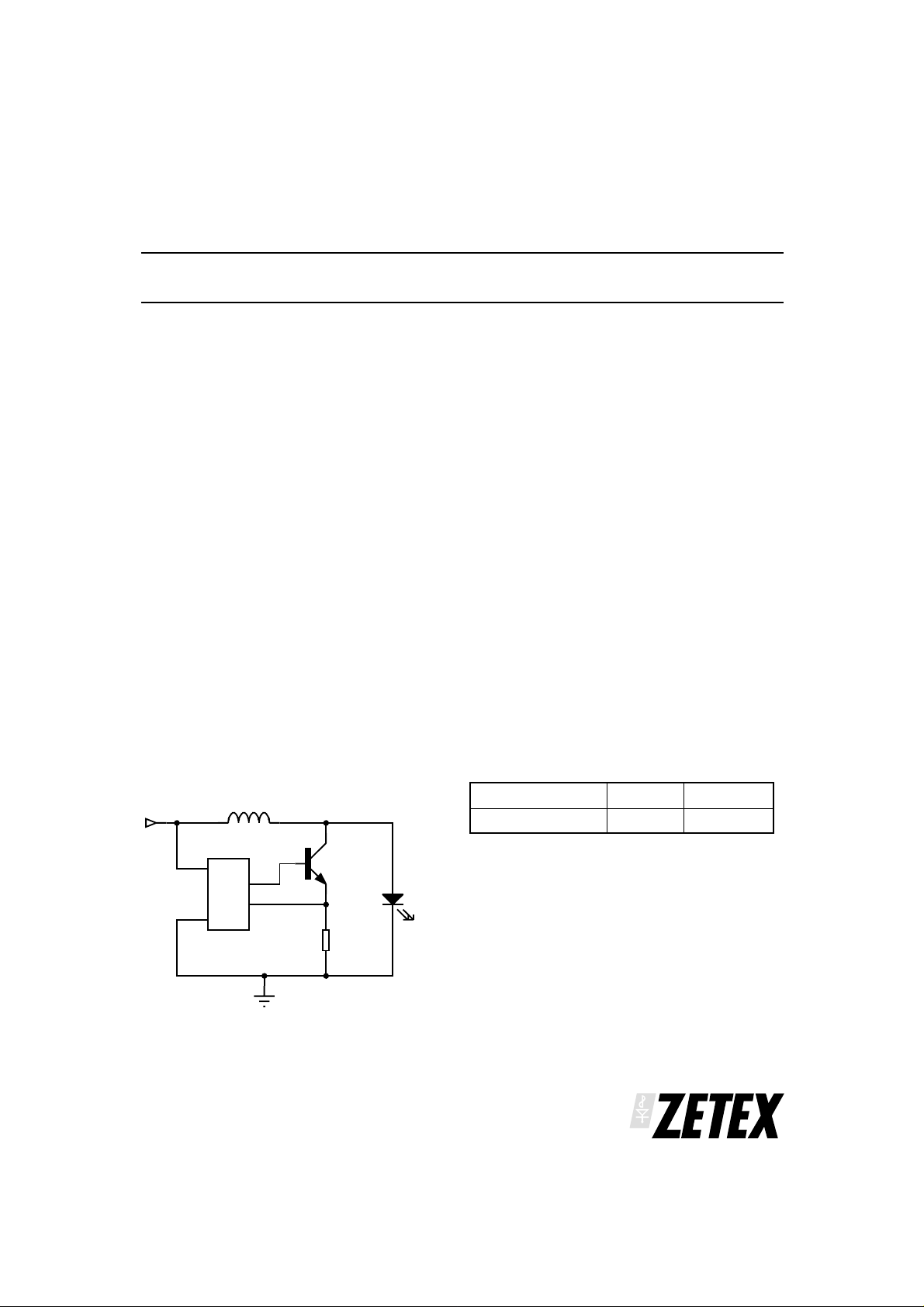
TYPICAL APPLICATION CIRCUIT
V
BATT
L1
100µH
U1
V
cc
V
drive
I
sense
Gnd
ZXSC300
ISSUE 1 - JUNE 2001
Q1
FMMT617
R1
0.33R
LED1
WHITE LED
ORDERING INFORMATION
DEVICE Package Partmarking
ZXSC300E5 SOT23-5 C300
1
Page 2
ZXSC300
ABSOLUTE MAXIMUM RATING
Supply Voltage -0.3 to 10V
Maximum Voltage Other Pins -0.3 to V
Power Dissipation 450mW
ELECTRICAL CHARACTERISTICS:
Test conditions unless otherwise stated: V
CC
+0.3V
Operating Temperature -40 to 85°C
Storage Temperature -55 to 125°C
=1.5V, T
CC
AMB
=25°C
Symbol Parameter Conditions Min Typ Max Units
η
V
CC
Efficiency
Recommended
supply voltage
1
0.8 8 V
94 %
range
V
CC(min)
I
Q
I
VDRIVE
I
CC
V
VDRIVE(high)
V
VDRIVE(low)
V
ISENSE
(threshold)
T
CVISENSE
I
ISENSE
ELECTRICAL CHARACTERISTICS: AC PARAMETERS
Minimum startup
and operating
voltage
Quiescent current
2
Base drive current V
Supply current
3
High level drive
voltage
Low level drive
voltage
Output current
reference voltage
I
SENSE
voltage temp co.
I
input current V
SENSE
2
I
DRIVE
I
DRIVE
T
AMB
DRIVE
V
DRIVE
V
ISENSE
V
ISENSE
ISENSE
=-600µA, V
=-600µA, V
3
=-10°C
DRIVE
DRIVE
=0.7V
=0.7V,
0.8
0.9
0.92 V
0.2 mA
= 0.7V, V
= 0.7V, V
= 0V, I
= 50mV, I
VDRIVE
= 0V 1.5 3.6 mA
ISENSE
=0V 2 4 mA
ISENSE
=-0.5mA VCC-0.3 V
= 5mA 0 0.2 V
VDRIVE
CC
14 19 24 mV
0.4 %/°C
= 0V 0 -30 -65 µA
2
TEST CONDITIONS (Unless otherwise stated) )
V
=1.5V, T
CC
= 0 to 70°C
AMB
V
Symbol Parameter Conditions Min Typ Max Units
T
DRV
F
OSC
1
Application dependent, see reference designs.
2
These parameters guaranteed by Design
3
Total supply current =IQ+ I
4
Operating frequency is application circuit dependent. See applications section.
Discharge Pulse Width 1.2 1.7 3.2 µs
Recommended operating
frequency
4
, see typical characteristics
VDRIVE
200 kHz
ISSUE 1 - JUNE 2001
2
Page 3
ZXSC300
FMMT617
For the circuits described in the applications section, ZetexFMMT617 is the recommended pass transistor. The
following indicates outline data for the transistor, more detailed information can be found in the Zetex surface
mount data book or at www.zetex.com
ELECTRICAL CHARACTERISTICS (at TA= 25°C unless otherwise stated).
PARAMETER SYMBOL MIN. TYP. MAX. UNIT CONDITIONS.
Collector-Emitter
Saturation Voltage
V
CE(sat)
8
70
150
Collector-Emitter
Breakdown Voltage
*Measured under pulsed conditions. Pulse width=300µs. Duty cycle ≤ 2%
V
(BR)CEO
15 18 V IC=10mA*
14
100
200
mV
mV
mV
I
=0.1A, IB=10mA*
C
I
=1A, IB=10mA*
C
I
=3A, IB=40mA*
C
ZHCS1000
For the circuits described in the applications section Zetex ZHCS1000 is the recommended Schottky diode. The
following indicates outline data for the diode, more detailed information is available at www.zetex.com
ELECTRICAL CHARACTERISTICS (at T
PARAMETER SYMBOL MIN. TYP. MAX. UNIT CONDITIONS.
Forward Voltage V
Reverse Current I
Reverse Recovery
Time
F
R
t
rr
= 25°C unless otherwise stated).
amb
400
500mVmV
50 100
µA
IF=500mA
I
VR=30V
12 ns Switched from IF= 500mA
to I
at I
=1A
F
= 500mA. Measured
R
=50mA
R
ISSUE 1 - JUNE 2001
3
3
Page 4
ZXSC300
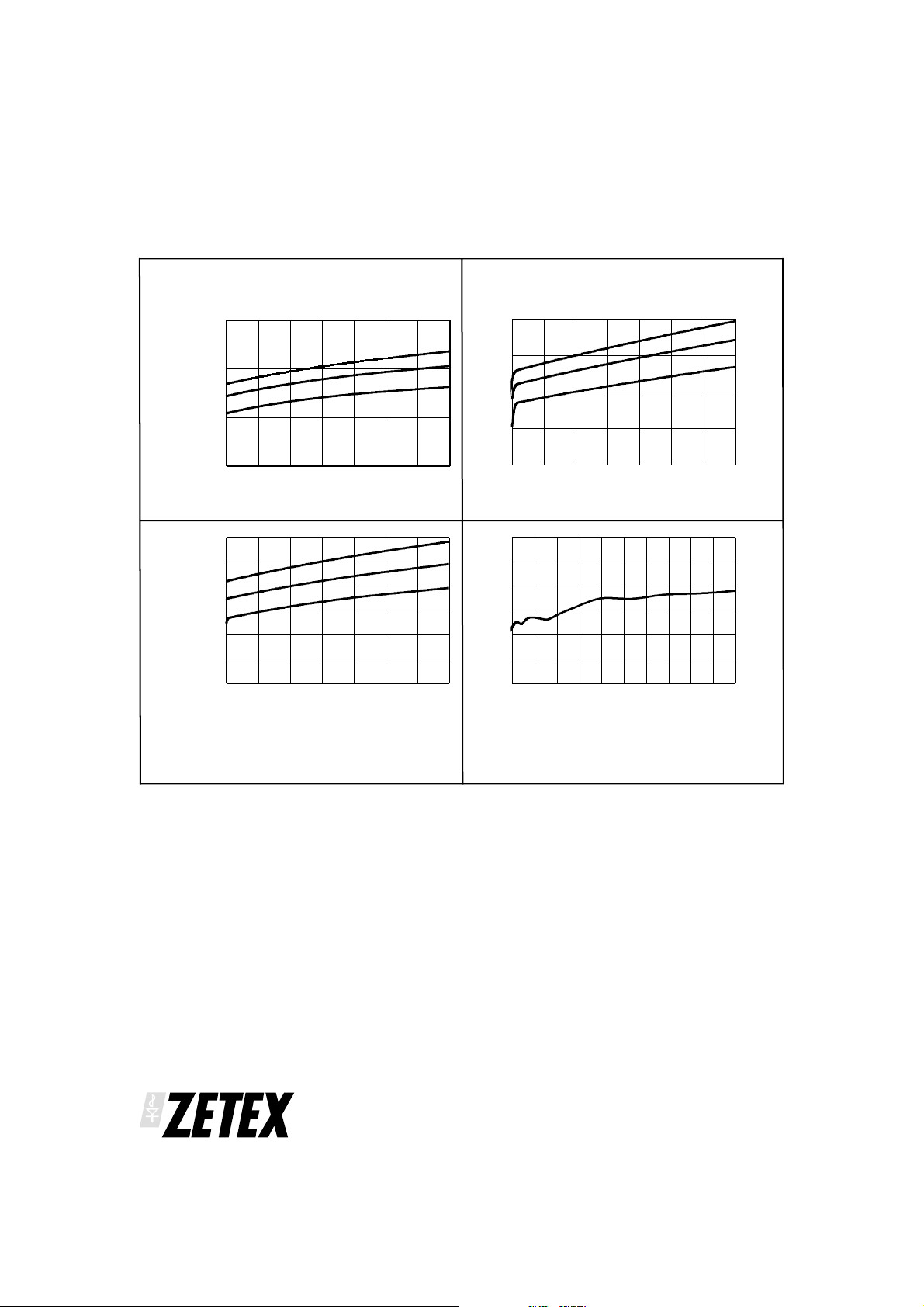
TYPICAL CHARACTERISTICS
300µ
200µ
100µ
Quiescent Current (A)
0
12345678
Input Voltage (V)
Quiescent Current v Input Voltage
30m
25m
20m
15m
10m
5m
Sense Voltage (V)
0
12345678
Input Voltage (V)
Sense Voltage v Input Voltage
4m
3m
2m
1m
Drive Current (A)
0
12345678
Input Voltage (V)
Drive Current v I nput Voltage
100
95
90
Efficiency (%)
85
1.0 1.5 2.0 2.5 3.0 3.5
Input Voltage (V)
Input Voltage v Efficiency
ISSUE 1 - JUNE 2001
4
Page 5

ZXSC300
DEVICE DESCRIPTION
The ZXSC300 is PFM, controller IC which, when
combined with a high performance external
transistor, enables the production of a high efficiency
boost converter for use in single cell LED driving
applications. A block diagram is shown for the
ZXSC300 in Figure 1.
Figure 1
ZXSC300 Block Diagram
The on chip comparator forces the driver circuit and
therefore the external switching transistor off if the
voltage at I
by an internal reference circuit and divider.
The Voltage at I
resistor connected in series with the emitter of the
switching transistor. A monostable following the
outputof thecomparatorforces theturn-offtime ofthe
output stage to be typically 1.7µs. This ensures that
there is sufficient time to discharge the inductor coil
before the next on period.
exceeds 19mV. This threshold is set
SENSE
is taken from a current sense
SENSE
Pin Descriptions
With every on pulse the switching transistor is kept on
until the voltage across the current-sense resistor
exceedsthe threshold oftheI
length, and therefore the switching frequency, is
determined by the programmed peak current, the
input voltage and the input to output voltage
differential. See applications section for details.
The Driver circuit supplies the external switching
transistor with a fixed drive current. To maximise
efficiency the external transistor switched quickly,
typically being forced off within 30ns.
input.The on-pulse
SENSE
Pin out Diagram
CC
ND
1
2
3
Top View
V
DRIVE
5
I
SENSE
4
V
G
Pin No. Name Description
1V
2 Gnd Ground
3 N/C Not connected
4I
5V
ISSUE 1 - JUNE 2001
CC
SENSE
DRIVE
Supply voltage, generally Alkaline, NiMH or NiCd single cell
Inductor current sense input. Internal threshold voltage set to 19mV.
Connect external sense resistor
Drive output for external switching transistor. Connect to base of
external switching transistor.
5
Page 6

ZXSC300
REFERENCE DESIGNS
Two typical LED driving applications are shown.
Firstly a maximum brightness solution and
secondly an optimised battery life solution.
Maximum brightness solution
This circuit provides a constant current output to
the LED by rectifying the switching pulses. This
ensures maximum LED brightness.
VBATT
L1
100µH
U1
V
cc
V
drive
I
sense
Gnd
ZXSC300
Q1
FMMT617
R1
0.1R
D1
ZHCS1000
C1
2.2µF
LED1
WHITE LED
Material List
Ref Value Part Number Manufacture Comments
U1 N/A ZXSC300E5 Zetex Plc Single cell converter, SOT23-5
Q1 N/A FMMT617 Zetex Plc Low V
D1 1A ZHCS1000 Zetex Plc 1A Shottky diode, SOT23
R1
C1
100mΩ
2.2µF
Generic Various 0805 Size
Generic Various Low ESR ceramic capacitor
L1 100µH DO1608P-104 Coilcraft Surface mount inductor
LED1 5600mcd NSPW500BS Nichia White LED
CE(sat)
NPN, SOT23
ISSUE 1 - JUNE 2001
6
Page 7

Maximum battery life solution
To ensure optimum efficiency, and therefore
maximum battery life, the LED is supplied with a
pulsed current. Maximum efficiency is ensured with
the removal of rectifier losses experienced in the
maximum brightness solution.
V
BATT
L1
100µH
U1
V
cc
V
drive
I
sense
Gnd
ZXSC300
Q1
FMMT617
R1
0.33R
LED1
WHITE LED
100
Single LED Load
95
90
Efficiency (%)
85
1.0 1.5 2.0 2.5 3.0 3.5
InputVoltage v Efficiency
ZXSC300
Input Voltage (V)
Materials list
Ref Value Part Number Manufacture Comments
U1 N/A ZXSC300E5 Zetex Plc Single cell converter, SOT23-5
Q1 N/A FMMT617 Zetex Plc Low V
R1
L1
330mΩ
100µH
Generic Various 0805 Size
DO1608P-104 Coilcraft Surface mount inductor
LED1 5600mcd NSPW500BS Nichia White LED
ISSUE 1 - JUNE 2001
7
CE(SAT)
NPN, SOT23
Page 8

ZXSC300
APPLICATIONS INFORMATION
The following section is a design guide for optimum
converter performance.
Switching transistor selection
The choice of switching transistor has a major impact
on the converter efficiency. For optimum
performance,a bipolar transistorwithlow V
high gain is required.
CE(SAT)
and
Schottky diode selection
For the maximum battery life solution a Schottky
rectifier diode is required. As with the switching
transistor the Schottky rectifier diode has a major
impact on the converter efficiency. A Schottky diode
with a low forward voltage and fast recovery time
should be used for this application.
The diode should be selected so that the maximum
forward current is greater or equal to the maximum
peakcurrent intheinductor, andthe maximumreverse
voltage is greater or equal to the output voltage.
The Zetex ZHCS1000 meets these needs. Datasheets
for the ZHCS Series are available on Zetex web site or
through your local Zetex sales office. Outline
informationis included inthecharacteristics section of
this data sheet.
Forthemaximum brightness solution a pulsedcurrent
is supplied to the LED therefore a Schottky rectifier
diode is not required.
Inductor selection
The inductor value must be chosen to satisfy
performance,costand size requirements of theoverall
solution. For the reference designs we recommend an
inductor value of 100uH with a core saturation current
rating greater than the converter peak current value
and low series resistance.
The Zetex FMMT617 is an ideal choice of transistor,
having a low saturation voltage. A data sheet for the
FMMT617 is available on Zetex web site or through
your local Zetex sales office. Outline information is
included in the characteristics section of this data
sheet.
Inductor selection has a significant impact on the
converter performance. For applications where
efficiency is critical, an inductor with a series
resistance of 500mΩ or less should be used.
Peak current definition
The peak current rating is a design parameter whose
value is dependent upon the overall application. For
the high brightness reference designs, a peak current
of was chosen to ensure that the converter could
provide the required output power to the LED.
In general, the I
the switching transistor, Q1, is in full saturation with
value must be chosen to ensure that
PK
maximum output power conditions, assuming
worse-case input voltage and transistor gain under all
operating temperature extremes.
Once I
determined by:
R
SENSE
where V
is decided the value of R
PK
V
ISENSE
=
I
PK
=19mV
ISENSE
SENSE
can be
ISSUE 1 - JUNE 2001
8
Page 9

ZXSC300
Output Power Calculation
By making the above assumptions for inductance and
peak current the output power can be determined by:
(V V x I I
P
=
OUT
Note: V
drop
OUT- IN PK MIN
= output voltage + Schottkyrectifier voltage
OUT
2
+)( )
T
x
()+
TT
ON OFF
OFF
where
T
≅ 1.7µs (internally set by ZXSC300)
OFF
and
TV V
T
=
ON
−()
OFF OUT IN
V
IN
and
II
=−
MIN PK
(V - V xT
OUT IN OFF
)
L
Operating frequency can be derived by:
F
1
=
TT
+
()
ON OFF
Layout of Maximum battery life solution
Capacitor selection
For pulsed operation, as in themaximum battery life
solution, no capacitors are required at the output to
the LED. For rectified operation, as in the maximum
brightness solution, a small value ceramic capacitor
is required, typically 2.2uF.
Generally an input capacitor is not required, but a
small ceramic capacitor may be added to aid EMC,
typically 470nF to 1uF.
Demonstration board
A demonstration board for the Maximum battery life
solution, is available upon request. These can be
obtained through your local Zetex office or through
Zetex web pages. For all reference designs Gerber
files and bill of materials can be supplied.
Top Copper
Drill Holes
Bottom Copper Silk Screen
ISSUE 1 - JUNE 2001
9
Page 10

ZXSC300
(Notes)
10
ISSUE 1 - JUNE 2001
Page 11

Supplier Listing
Zetex
AVX
Coilcraft
Nichia Corporation
ZXSC300
GERMANY ASIA USA UK
Zetex GmbH
Munich
(49) 894549490 (852) 2610 0611 (1) 631 543 7100 (44) 161 622 4444
http://www.zetex.com
http://www.avxcorp.com
http://www.coilcraft.com
Nichia Europe B.V.
Amsterdam
The Netherlands
(31) 20 5060900
http://www.nichia.co.jp
Zetex Asia
Hong Kong
AVX Asia
Singapore
(65) 258 2833
Nichia Corporation
Tokyo Sales Office
Tokyo, Japan
(81) 3 3456 3784
Zetex Inc
Long Island NY
AVX USA
(1) 843 448 9411
Coilcraft Inc
(1) 847 639 6400
Nichia America
Corporation
Head Office
(1) 717 285 2323
San Jose
(1) 408 573 0933
Zetex PLC
Chadderton,
Oldham
AVX UK
(44) 1252 770000
Coilcraft Europe
(44) 1236 730595
ISSUE 1 - JUNE 2001
11
Page 12

ZXSC300
ZXSC300
PACKAGE DIMENSIONS SOT23-5
DIM
Millimetres Inches
MIN MAX MIN MAX
A 0.90 1.45 0.035 0.057
A1 0.00 0.15 0.00 0.006
A2 0.90 1.3 0.035 0.051
b 0.35 0.50 0.014 0.020
C 0.09 0.20 0.0035 0.008
D 2.80 3.00 0.110 0.118
E 2.60 3.00 0.102 0.118
E1 1.50 1.75 0.059 0.069
e 0.95 REF 0.037 REF
e1 1.90 REF 0.075 REF
L 0.10 0.60 0.004 0.024
a° 010010
Zetex plc.
Fields New Road, Chadderton, Oldham, OL9-8NP, United Kingdom.
Telephone: (44)161 622 4422 (Sales), (44)161 622 4444 (General Enquiries)
Fax: (44)161 622 4420
Zetex GmbH Zetex Inc. Zetex (Asia) Ltd. These are supported by
Streitfeldstraße 19 47 Mall Drive, Unit 4 3701-04 Metroplaza, Tower 1 agents and distributors in
D-81673 München Commack NY 11725 Hing Fong Road, major countries world-wide
Germany USA Kwai Fong, Hong Kong © Zetex plc 2001
Telefon: (49) 89 45 49 49 0 Telephone: (631) 543-7100 Telephone:(852) 26100 611
Fax: (49) 89 45 49 49 49 Fax: (631) 864-7630 Fax: (852) 24250 494 www.zetex.com
This publication is issued to provide outline information only which (unless agreed by the Company in writing) may not be used, applied or
reproduced for any purpose or form part of any order or contract or be regarded as a representation relating to the products or services
concerned. The Company reserves the right to alter without notice the specification, design, price or conditions of supply of any product or
service.
Publication Ref. SCZXSC300DS
ISSUE 1 - JUNE 2001
12
 Loading...