

Page 1
200V P-CHANNEL ENHANCEMENT MODE MOSFET
SUMMARY
(BR)DSS
=-200V; R
V
DESCRIPTION
This 200V enhancement mode P-channel MOSFET provides users with a
competitive specification offering efficient power handling capability, high
impedance and is free from thermal runaway and thermally induced
secondary breakdown. Applications benefiting from this device include a
variety of Telecom and general high voltage circuits.
= 28 ; ID= -122mA
DS(ON)
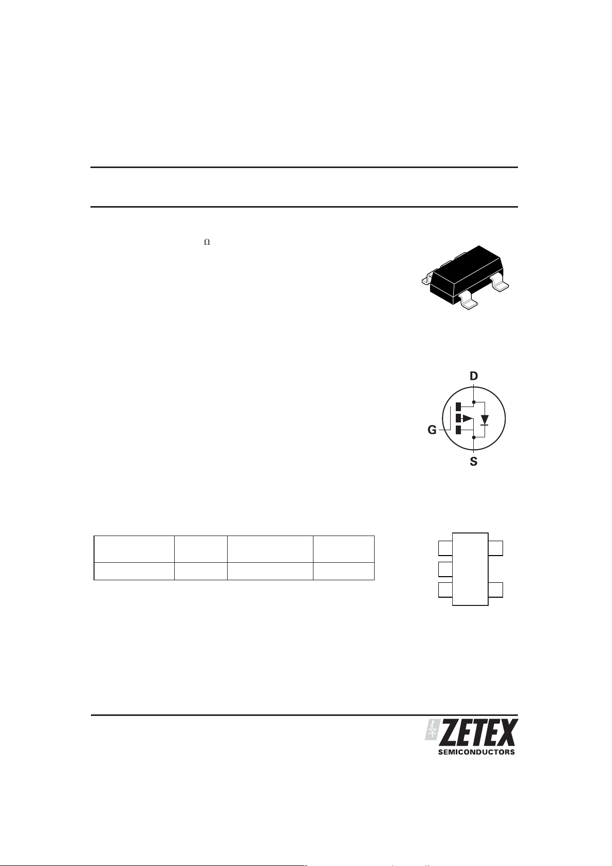
ZXMP2120E5
A 4 pin SOT223 version is also available (ZXMP2120G4).
FEATURES
High voltage
•
Low on-resistance
•
Fast switching speed
•
Low gate drive
•
•
Low threshold
•
SOT23-5 package variant engineered to increase spacing between
high voltage pins.
APPLICATIONS
•
Active clamping of primary side MOSFETs in 48 volt DC-DC converters
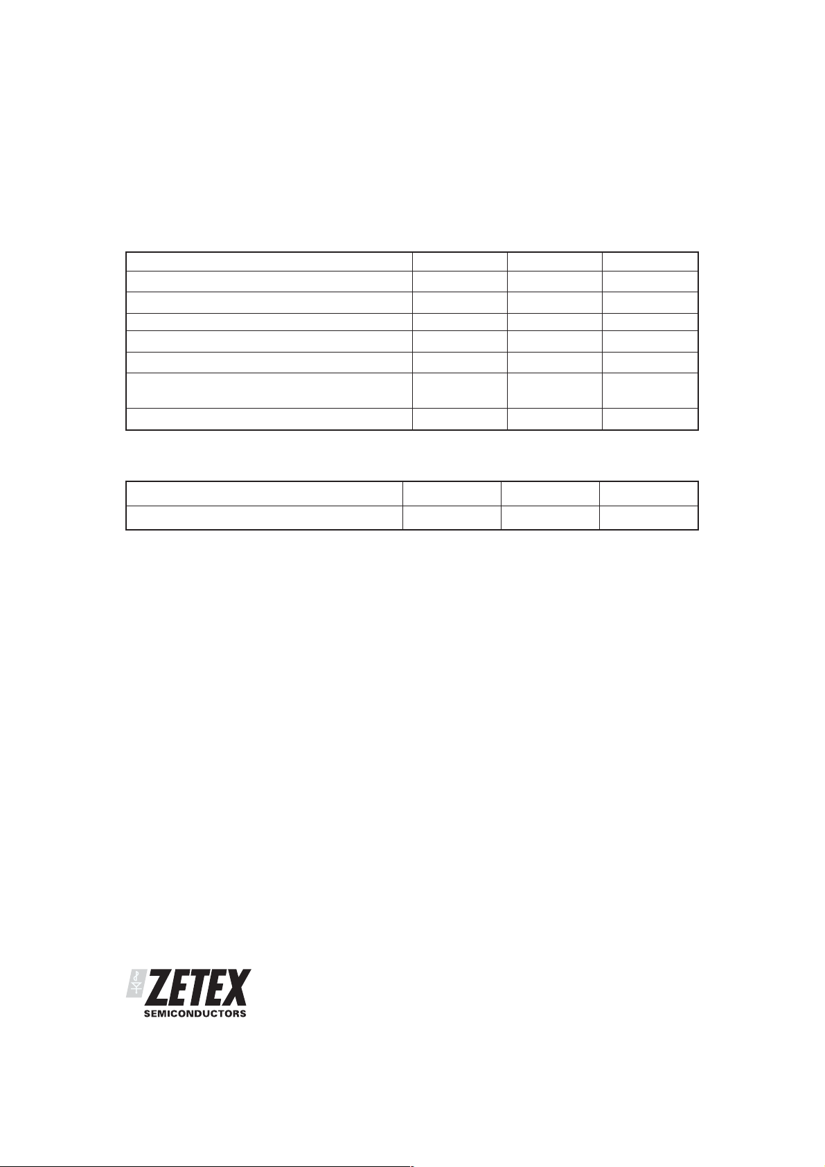
ORDERING INFORMATION
DEVICE REEL SIZE
ZXMP2120E5TA 7 8mm embossed 3,000 units
DEVICE MARKING
•
P120
(inches)
TAPE WIDTH (mm) QUANTITY
PER REEL
SOT23-5
N/C
D
N/C
PINOUT - TOP VIEW
S
G
ISSUE 2 - SEPTEMBER 2006
1
Page 2
ZXMP2120E5
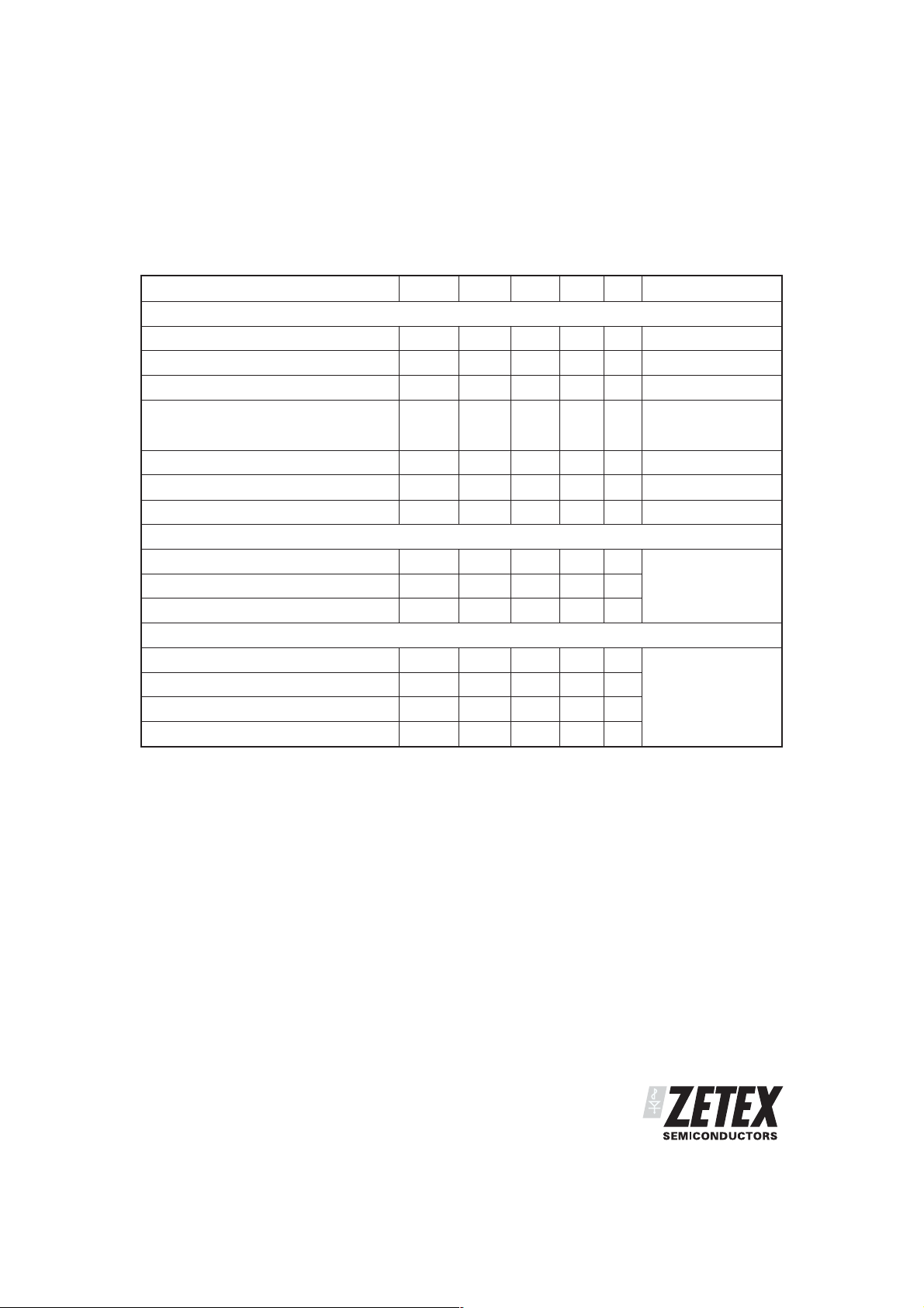
ABSOLUTE MAXIMUM RATINGS
PARAMETER SYMBOL LIMIT UNIT
V
(a)
I
I
I
P
DSS
GS
D
DM
SM
D
Drain-Source Voltage
Gate Source Voltage V
Continuous Drain Current (V
=10V; T
GS
amb
=25°C)
Pulsed Drain Current (c)
Pulsed Source Current (Body Diode)
Power Dissipation at T
amb
=25°C
(c)
(a)
Linear Derating Factor
Operating and Storage Temperature Range T
j:Tstg
THERMAL RESISTANCE
PARAMETER SYMBOL VALUE UNIT
Junction to Ambient
NOTES
(a) For a device surface mounted on 25mm x 25mm FR4 PCB with high coverage of single sided 1oz copper, in still air conditions
(b) For a device surface mounted on FR4 PCB measured at t⭐5 secs.
(c) Repetitive rating - pulse width limited by maximum junction temperature. Refer to Transient Thermal Impedance graph.
(a)
R
θJA
-200 V
±20
-122 mA
-0.7 A
-0.7 A
0.75
6
W
mW/°C
-55 to +150 °C
167 °C/W
V
ISSUE 2 - SEPTEMBER 2006
2
Page 3
ZXMP2120E5
ELECTRICAL CHARACTERISTICS (at T
= 25°C unless otherwise stated)
amb
PARAMETER SYMBOL MIN. TYP. MAX. UNIT CONDITIONS.
STATIC
Drain-Source Breakdown Voltage V
Gate-Source Threshold Voltage V
Gate-Body Leakage I
Zero Gate Voltage Drain Current I
On-State Drain Current
Static Drain-Source On-State Resistance
Forward Transconductance
(1)
(1)
(1)(2)
(BR)DSS
GS(th)
GSS
DSS
I
D(on)
R
DS(on)
g
fs
-200 V ID=-1mA, VGS=0V
-1.5 -3.5 V ID=-1mA, VDS=V
20 nA VGS= ⫾20V, VDS=0V
-10
-100AµA
VDS=-200 V, VGS=0
V
=-160 V, VGS=0V,
DS
T=125°C
(2)
-300 mA VDS=-25 V, VGS=-10V
28
VGS=-10V, ID=-150mA
Ω
50 mS VDS=-25V,ID=-150mA
DYNAMIC
Input Capacitance
Output Capacitance
Reverse Transfer Capacitance
(2)
(2)
(2)
C
iss
C
oss
C
rss
100 pF
25 pF
7pF
V
=-25 V, VGS=0V,
DS
f=1MHz
SWITCHING
Turn-On Delay Time
Rise Time
(2)(3)
Turn-Off Delay Time
Fall Time
NOTES:
(1) Measured under pulsed conditions. Width=300µs. Duty cycle ≤ 2%.
(2) Sample test.
(3) Switching times measured with 50Ω source impedance and <5ns rise time on a pulse generator.
(2)(3)
(2) (3)
(2) (3)
t
d(on)
t
r
t
d(off)
t
f
7ns
15 ns
12 ns
15 ns
V
=-25V, ID=-150mA
DD
GS
ISSUE 2 - SEPTEMBER 2006
3
Page 4

ZXMP2120E5
TYPICAL CHARACTERISTICS
ISSUE 2 - SEPTEMBER 2006
4
Page 5

CHARACTERISTICS
ZXMP2120E5
ISSUE 2 - SEPTEMBER 2006
5
Page 6

ZXMP2120E5
PACKAGE OUTLINE
PAD LAYOUT DETAILS
0.95
0.375
2.2
0.087
0.65
0.025
Controlling dimensions are in millimeters. Approximate conversions are given in inches
PACKAGE DIMENSIONS
DIM
Millimeters Inches
MIN. MAX. MIN. MAX.
A 0.90 1.45 0.0354 0.0570
A1 - 0.15 - 0.0059
A2 0.90 1.30 0.0354 0.0511
b 0.20 0.50 0.0078 0.0196
C 0.09 0.26 0.0035 0.0102
D 2.70 3.10 0.1062 0.1220
DIM
E 2.20 3.20 0.0866 0.1181
E1 1.30 1.80 0.0511 0.0708
e 0.95 REF 0.0374 REF
e1 1.90 REF 0.0748 REF
L 0.10 0.60 0.0039 0.0236
a 0° 30° 0° 30°
Millimeters Inches
MIN. MAX. MIN. MAX.
1.06
0.042
mm
inches
© Zetex Semiconductors plc 2006
Europe
Zetex GmbH
Kustermann-park
Balanstraße 59
D-81541 München
Germany
Telefon: (49) 89 45 49 49 0
Fax: (49) 89 45 49 49 49
europe.sales@zetex.com
These offices are supported by agents and distributors in major countries world-wide.
This publicationis issued toprovide outline informationonly which (unless agreed by the Company inwriting) may notbe used, appliedor reproduced
for any purposeor form part of any order or contract or be regarded as a representation relating to the products or services concerned. The Company
reserves the right to alter without notice the specification, design, price or conditions of supply of any product or service.
For the latest product information, log on to www.zetex.com
Americas
Zetex Inc
700 Veterans Memorial Hwy
Hauppauge, NY 11788
USA
Telephone: (1) 631 360 2222
Fax: (1) 631 360 8222
usa.sales@zetex.com
Asia Pacific
Zetex (Asia) Ltd
3701-04 Metroplaza Tower 1
Hing Fong Road, Kwai Fong
Hong Kong
Telephone: (852) 26100 611
Fax: (852) 24250 494
asia.sales@zetex.com
Corporate Headquarters
Zetex Semiconductors plc
Zetex Technology Park
Chadderton, Oldham, OL9 9LL
United Kingdom
Telephone (44) 161 622 4444
Fax: (44) 161 622 4446
hq@zetex.com
ISSUE 2 - SEPTEMBER 2006
6
Page 7

 Loading...