

Page 1
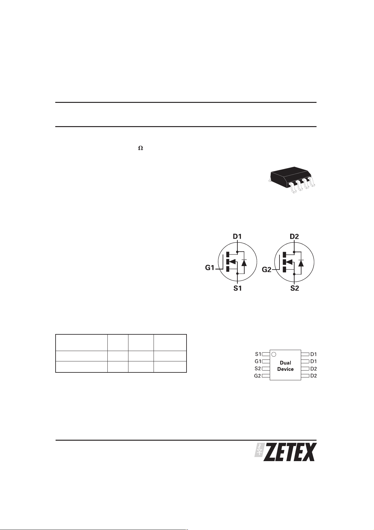
60V N-CHANNEL ENHANCEMENT MODE MOSFET
ZXMN6A11DN8
SUMMARY
V
(BR)DSS
= 60V; R
= 0.14 ID= 2.7A
DS(ON)
DESCRIPTION
This new generation of TRENCH MOSFETs from Zetex utilises a unique structure
that combines the benefits of low on-resistance with fast switching speed. This
makes them ideal for high efficiency, low voltage, power management applications.
FEATURES
Low on-resistance
•
Fast switching speed
•
Low threshold
•
Low gate drive
•
Low profile SO8 package
•
APPLICATIONS
•
DC - DC Converters
•
Power Management Functions
•
Disconnect switches
•
Motor control
SO8
ORDERING INFORMATION
DEVICE REEL
SIZE
ZXMN6A11DN8TA 7” 12mm 500 units
ZXMN6A11DN8TC 13” 12mm 2500 units
TAPE
WIDTH
QUANTITY
PER REEL
DEVICE MARKING
•
ZXMN
6A11D
ISSUE 1 - MARCH 2002
Top View
1
Page 2
ZXMN6A11DN8
ABSOLUTE MAXIMUM RATINGS
PARAMETER SYMBOL LIMIT UNIT
Drain-Source Voltage V
Gate Source Voltage V
Continuous Drain Current VGS=10V; TA=25°C(b)
VGS=10V; TA=70°C(b)
VGS=10V; TA=25°C(a)
Pulsed Drain Current (c) I
Continuous Source Current (Body Diode) (b) I
Pulsed Source Current (Body Diode)(c) I
Power Dissipation at TA=25°C (a)(d)
Linear Derating Factor
Power Dissipation at TA=25°C (a)(e)
Linear Derating Factor
Power Dissipation at TA=25°C (b)(d)
Linear Derating Factor
Operating and Storage Temperature Range Tj:T
THERMAL RESISTANCE
I
D
DM
S
SM
P
P
P
DSS
GS
D
D
D
stg
60 V
⫾20 V
2.7
2.2
2.1
8.3 A
3.2 A
8.3 A
1.25
10
1.8
14
2.1
17
-55 to +150 °C
mW
mW/°C
mW
mW/°C
mW
mW/°C
A
PARAMETER SYMBOL VALUE UNIT
Junction to Ambient (a)(d)
Junction to Ambient (a)(e)
Junction to Ambient (b)(d)
NOTES
(a) For a device surface mounted on 25mm x 25mm FR4 PCB with high coverage of single sided 1oz copper, in still air conditions
(b) For a device surface mounted on FR4 PCB measured at t⭐10 secs.
(c) Repetitive rating 25mm x 25mm FR4 PCB, D=0.05 pulse width=10µs - pulse width limited by maximum junction temperature.
(d) For device with one active die
(e) For device with two active die running at equal power.
R
R
R
θJA
θJA
θJA
100 °C/W
70 °C/W
60 °C/W
ISSUE 1 - MARCH 2002
2
Page 3
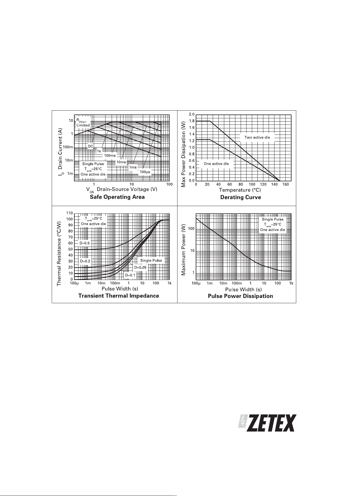
CHARACTERISTICS
ZXMN6A11DN8
ISSUE 1 - MARCH 2002
3
Page 4

ZXMN6A11DN8
ELECTRICAL CHARACTERISTICS (at TA = 25°C unless otherwise stated)
PARAMETER SYMBOL MIN. TYP. MAX. UNIT CONDITIONS.
STATIC
Drain-Source Breakdown Voltage V
Zero Gate Voltage Drain Current I
Gate-Body Leakage I
Gate-Source Threshold Voltage V
Static Drain-Source On-State
Resistance (1)
Forward Transconductance (3) g
DYNAMIC (3)
Input Capacitance C
Output Capacitance C
Reverse Transfer Capacitance C
SWITCHING(2) (3)
Turn-On Delay Time t
Rise Time t
Turn-Off Delay Time t
Fall Time t
Gate Charge Q
Total Gate Charge Q
Gate-Source Charge Q
Gate-Drain Charge Q
SOURCE-DRAIN DIODE
Diode Forward Voltage (1) V
Reverse Recovery Time (3) t
Reverse Recovery Charge (3) Q
NOTES
(1) Measured under pulsed conditions. Width≤300µs. Duty cycle ≤ 2% .
(2) Switching characteristics are independent of operating junction temperature.
(3) For design aid only, not subject to production testing.
(BR)DSS
DSS
GSS
GS(th)
R
DS(on)
fs
iss
oss
rss
d(on)
r
d(off)
f
g
g
gs
gd
SD
rr
rr
60 V
1 AVDS=60V, VGS=0V
100 nA VGS=⫾20V, VDS=0V
1.0 V ID=250A, VDS=V
0.14
0.25
4.9 S VDS=15V,ID=2.5A
330 pF
35.0 pF
17.0 pF
1.95 ns
3.5 ns
8.2 ns
4.6 ns
3.0 nC VDS=15V, VGS=5V,
5.7 nC VDS=15V,VGS=10V,
1.25 nC
0.86 nC
0.85 0.95 V TJ=25°C, IS=2.8A,
21.5 ns TJ=25°C, IF=2.5A,
20.5 nC
ID=250µA, VGS=0V
VGS=10V, ID=4.4A
⍀
VGS=4.5V, ID=3.8A
⍀
VDS=40V,VGS=0V,
f=1MHz
VDD=15V, ID=2.5A
RG=6.0⍀,VGS=10V
(refer to test circuit)
ID=2.5A
=2.5A
I
D
(refer to test circuit)
VGS=0V
di/dt= 100A/µs
GS
ISSUE 1 - MARCH 2002
4
Page 5

TYPICAL CHARACTERISTICS
ZXMN6A11DN8
ISSUE 1 - MARCH 2002
5
Page 6

ZXMN6A11DN8
TYPICAL CHARACTERISTICS
ISSUE 1 - MARCH 2002
6
Page 7

ZXMN6A11DN8
PACKAGE DIMENSIONSPACKAGE OUTLINE
DIM
INCHES
MIN MAX
A 0.053 0.069
A1 0.004 0.010
D 0.189 0.197
H 0.228 0.244
E 0.150 0.157
L 0.016 0.050
e 0.050 BSC
b 0.013 0.020
c 0.008 0.010
⍜ 0⬚ 8⬚
h 0.010 0.020
© Zetex plc 2002
Zetex plc
Fields New Road
Chadderton
Oldham, OL9 8NP
United Kingdom
Telephone (44) 161 622 4422
Fax: (44) 161 622 4420
These offices are supported by agents and distributors in major countries world-wide.
This publicationis issued toprovide outline informationonly which (unlessagreed by theCompany in writing)may not beused, applied orreproduced
for any purposeorformpartofanyorderorcontract or be regarded as arepresentationrelatingtotheproductsorservicesconcerned. The Company
reserves the right to alter without notice the specification, design, price or conditions of supply of any product or service.
For the latest product information, log on to
Zetex GmbH
Streitfeldstraße 19
D-81673 München
Germany
Telefon: (49) 89 45 49 49 0
Fax: (49) 89 45 49 49 49
www.zetex.com
Zetex Inc
700 Veterans Memorial Hwy
Hauppauge, NY11788
USA
Telephone: (631) 360 2222
Fax: (631) 360 8222
Zetex (Asia) Ltd
3701-04 Metroplaza, Tower 1
Hing Fong Road
Kwai Fong
Hong Kong
Telephone: (852) 26100 611
Fax: (852) 24250 494
ISSUE 1 - MARCH 2002
7
 Loading...