

Page 1
40V N-CHANNEL ENHANCEMENT MODE MOSFET
SUMMARY
V
(BR)DSS
DESCRIPTION
This new generation of TRENCH MOSFETs from Zetex utilizes a unique structure
that combines the benefits of low on-resistance with fast switching speed. This
makesthemidealforhighefficiency,lowvoltage,powermanagementapplications.
= 40V; R
= 0.05 ID= 7A
DS(ON)
ZXMN4A06G
FEATURES
Low on-resistance
•
Fast switching speed
•
Low threshold
•
Low gate drive
•
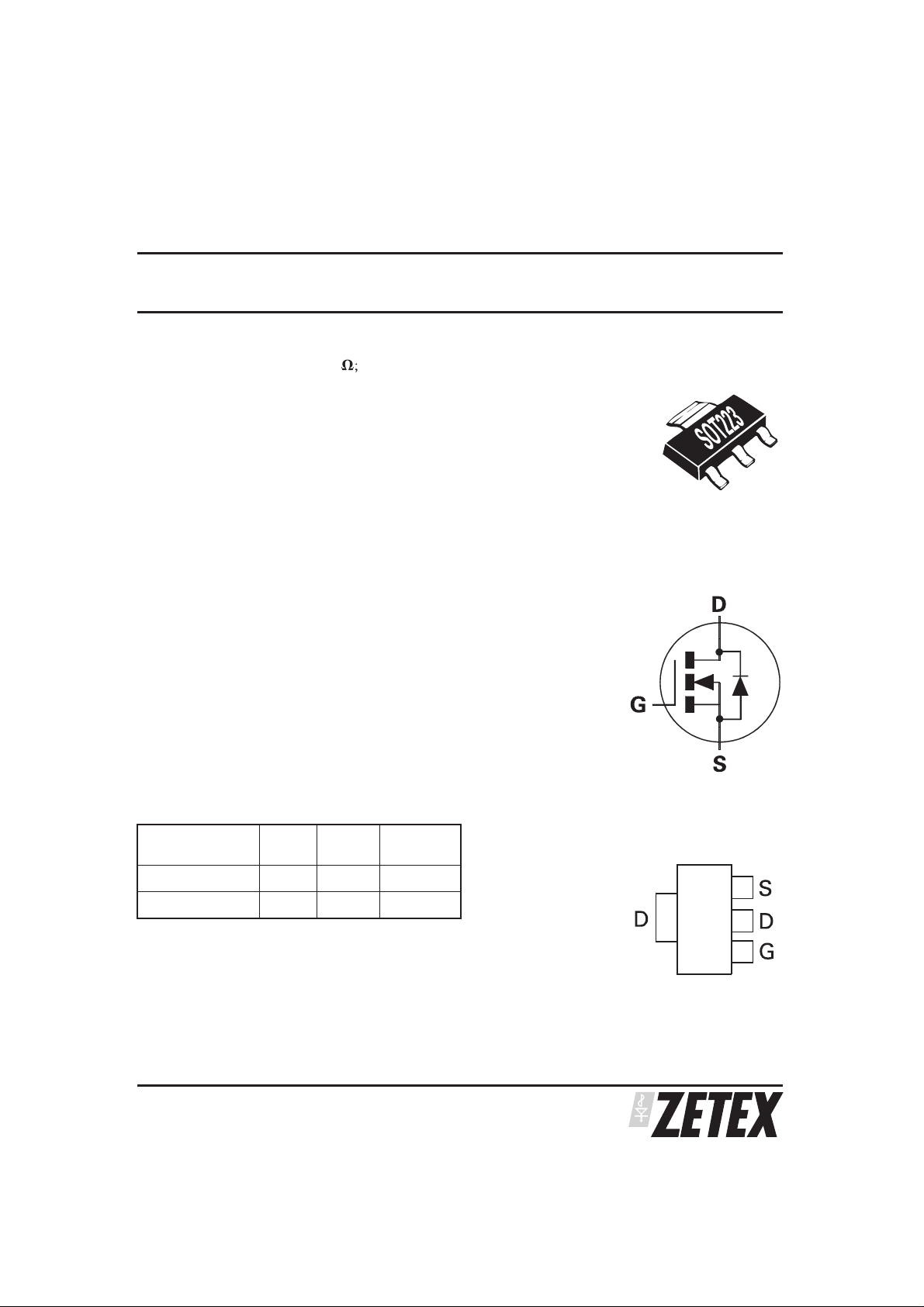
SOT223 package
•
APPLICATIONS
•
DC - DC Converters
•
Audio Output Stages
•
Relay and Solenoid driving
•
Motor control
ORDERING INFORMATION
DEVICE REEL
SIZE
ZXMN4A06GTA 7” 12mm 1000 units
ZXMN4A06GTC 13” 12mm 4000 units
TAPE
WIDTH
QUANTITY
PER REEL
DEVICE MARKING
•
ZXMN
4A06
SOT223
Top View
ISSUE 1 - MAY 2002
1
Page 2
ZXMN4A06G
ABSOLUTE MAXIMUM RATINGS
PARAMETER SYMBOL LIMIT UNIT
Drain-Source Voltage V
Gate-Source Voltage V
Continuous Drain Current V
=10V; TA=25°C(b)
GS
V
=10V; TA=70°C(b)
GS
V
=10V; TA=25°C(a)
GS
Pulsed Drain Current (c) I
Continuous Source Current (Body Diode) (b) I
Pulsed Source Current (Body Diode)(c) I
Power Dissipation at T
Linear Derating Factor
Power Dissipation at T
Linear Derating Factor
=25°C (a)
A
=25°C (b)
A
Operating and Storage Temperature Range T
THERMAL RESISTANCE
I
D
DM
S
SM
P
P
DSS
GS
D
D
j:Tstg
40 V
20 V
7.0
5.6
5.0
22 A
5.4 A
22 A
2.0
16
mW/°C
3.9
31
mW/°C
-55 to +150 °C
A
W
W
PARAMETER SYMBOL VALUE UNIT
Junction to Ambient (a) R
Junction to Ambient (b) R
NOTES
(a) For a device surface mounted on 25mm x 25mm FR4 PCB with high coverage of single sided 1oz copper, in still air conditions
(b) For a device surface mounted on FR4 PCB measured at t⭐5 secs.
(c) Repetitive rating 25mm x 25mm FRA PCB, D=0.05 pulse width = 10s - pulse width limited by maximum junction temperature.
θJA
θJA
62.5 °C/W
32.2 °C/W
ISSUE 1 - MAY 2002
2
Page 3
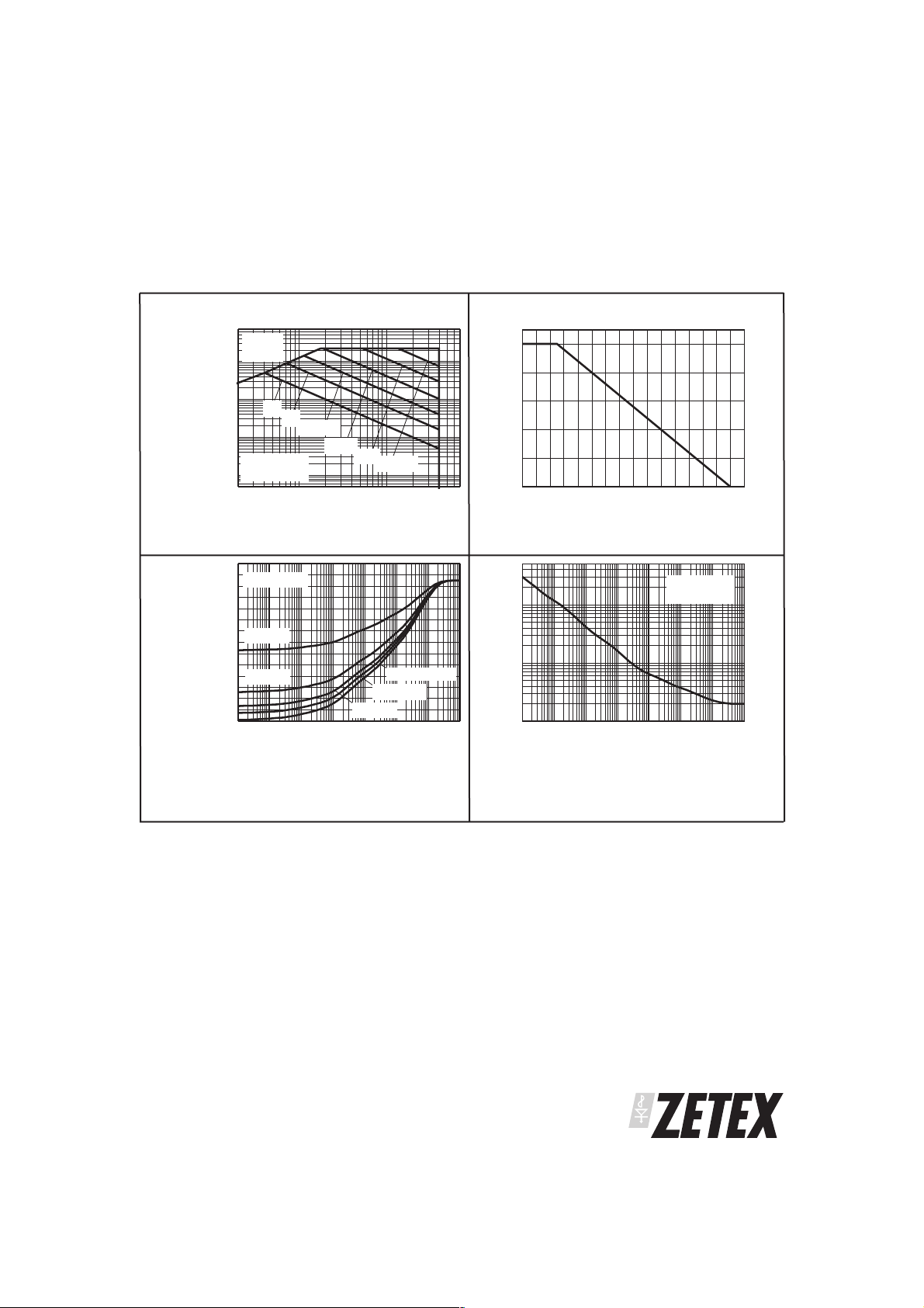
CHARACTERISTICS
ZXMN4A06G
R
DS(on)
Limi ted
10
1
DC
1s
100m
Single Pulse
Drain Current (A)
T
amb
10m
D
I
VDSDrain-Source Voltage (V)
100ms
10ms
1ms
= 25° C
110
100µs
Safe Operating Area
70
T
=25°C
amb
60
50
40
D= 0.5
30
20
D= 0.2
10
0
100µ 1m 10m100m 1 10 100 1k
Thermal Resistance (° C/W)
Transient Thermal Impedance
Pulse Width (s)
Single Pulse
D= 0.05
D= 0.1
2.0
1.6
1.2
0.8
0.4
0.0
0 20 40 60 80 100 120 140 160
Max Power Dissipation (W)
100
10
Maximum Power (W)
1
100µ 1m 10m100m 1 10 100 1k
Temperature (° C)
Derating Curve
Single Pulse
T
=25°C
amb
Pulse Width (s)
Pulse Power Dissipation
ISSUE 1 - MAY 2002
3
Page 4

ZXMN4A06G
ELECTRICAL CHARACTERISTICS (at TA = 25°C unless otherwise stated)
PARAMETER SYMBOL MIN. TYP. MAX. UNIT CONDITIONS.
STATIC
Drain-Source Breakdown Voltage V
Zero Gate Voltage Drain Current I
Gate-Body Leakage I
Gate-Source Threshold Voltage V
Static Drain-Source On-State
Resistance (1)
Forward Transconductance (3) g
DYNAMIC (3)
Input Capacitance C
Output Capacitance C
Reverse Transfer Capacitance C
SWITCHING(2) (3)
Turn-On Delay Time t
Rise Time t
Turn-Off Delay Time t
Fall Time t
Total Gate Charge Q
Gate-Source Charge Q
Gate-Drain Charge Q
SOURCE-DRAIN DIODE
Diode Forward Voltage (1) V
Reverse Recovery Time (3) t
Reverse Recovery Charge (3) Q
(BR)DSS
DSS
GSS
GS(th)
R
DS(on)
fs
iss
oss
rss
d(on)
r
d(off)
f
g
gs
gd
SD
rr
rr
40 V ID=250A, VGS=0V
1 AVDS=40V, VGS=0V
100 nA
V
=±20V, VDS=0V
GS
1.0 V ID=250A, VDS=V
0.050
0.075
VGS=10V, ID=4.5A
⍀
V
⍀
=4.5V, ID=3.2A
GS
8.7 S VDS=15V,ID=2.5A
770 pF
V
=40V,VGS=0V,
92 pF
DS
f=1MHz
61 pF
2.55 ns
V
4.45 ns
28.61 ns
=30V, ID=2.5A
DD
R
=6.0⍀,VGS=10V
G
(refer to test circuit)
7.35 ns
18.2 nC
2.1 nC
4.5 nC
=30V,VGS=10V,
V
DS
I
=2.5A
D
(refer to test circuit)
0.8 0.95 V TJ=25°C, IS=2.5A,
V
=0V
GS
19.86 ns TJ=25°C, IF=2.5A,
16.36 nC
di/dt= 100A/µs
GS
NOTES
(1) Measured under pulsed conditions. Width≤300µs. Duty cycle ≤ 2% .
(2) Switching characteristics are independent of operating junction temperature.
(3) For design aid only, not subject to production testing.
4
ISSUE 1 - MAY 2002
Page 5

TYPICAL CHARACTERISTICS
ZXMN4A06G
T= 25°C
10
1
Drain Current (A)
0.1
D
I
0.1 1 10
VDSDrain-Source Voltage (V)
10V
4V
3.5V
3V
2.5V
V
GS
2V
Output Characteristics
10
T = 150° C
T = 25° C
1
Drain Current (A)
D
I
VDS=10V
1234
VGSGate-Source Voltage (V)
Typical Transfer Characteristics
1.5V
10
2V
V
GS
1
T = 25° C
2.5V
3V
3.5V
T = 150° C
10V
10
1
Drain Current (A)
0.1
D
I
0.1 1 10
VDSDrain-Source Voltage (V)
4V
3.5V
3V
2.5V
2V
V
1.5V
GS
Output Characteristics
1.8
1.6
GS(th)
1.4
and V
1.2
DS(on)
1.0
0.8
0.6
Normalised R
0.4
-50 0 50 100 150
VGS= 10V
I
=4.5A
D
VGS=V
DS
ID=250uA
R
V
DS(on)
GS(th)
Tj Junction Temperature (° C)
Normalised Curves v Tem perature
10
1
T = 150° C
T = 25° C
0.1
Drain-Source On-Resistance (Ω)
DS(on)
R
On-Resistance v Drain Current
ISSUE 1 - MAY 2002
110
IDDrain Current (A)
4V
10V
Reverse Drain Current (A)
0.1
SD
I
0.2 0.4 0.6 0.8 1.0 1.2 1.4
V
Source-Drain Voltage (V)
SD
Source-Drain Diode Forward Voltage
5
Page 6

ZXMN4A06G
TYPICAL CHARACTERISTICS
ISSUE 1 - MAY 2002
6
Page 7

ZXMN4A06G
PACKAGE OUTLINE
PACKAGE DIMENSIONS
MILLIMETRES
DIM
MIN MAX MIN MAX
A ᎏ 1.80 D 6.30 6.70
A1 0.02 0.10 e 2.30 BASIC
A2 1.55 1.65 e1 4.60 BASIC
b 0.66 0.84 E 6.70 7.30
b2 2.90 3.10 E1 3.30 3.70
C 0.23 0.33 L 0.90 ᎏ
MILLIMETRES
DIM
PAD LAYOUT DETAILS
4.6
2.3
6.8
3.8 min
2.0 min
(3x)
1.5 min
(3x)
2.0 min
© Zetex plc 2002
Zetex plc
Fields New Road
Chadderton
Oldham, OL9 8NP
United Kingdom
Telephone (44) 161 622 4422
Fax: (44) 161 622 4420
These offices are supported by agents and distributors in major countries world-wide.
Thispublication is issued to provide outline information only which (unless agreedby the Companyin writing) maynot be used,applied or reproduced
for any purpose or form part of any order or contract or be regarded as a representation relating to the products or services concerned. The Company
reserves the right to alter without notice the specification, design, price or conditions of supply of any product or service.
For the latest product information, log on to
Zetex GmbH
Streitfeldstraße 19
D-81673 München
Germany
Telefon: (49) 89 45 49 49 0
Fax: (49) 89 45 49 49 49
www.zetex.com
Zetex Inc
700 Veterans Memorial Hwy
Hauppauge, NY11788
USA
Telephone: (631) 360 2222
Fax: (631) 360 8222
Zetex (Asia) Ltd
3701-04 Metroplaza, Tower 1
Hing Fong Road
Kwai Fong
Hong Kong
Telephone: (852) 26100 611
Fax: (852) 24250 494
ISSUE 1 - MAY 2002
7
 Loading...