

Page 1
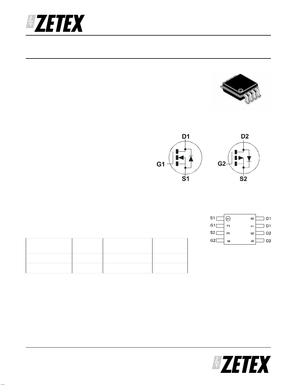
ZXMD63C02X
20V DUAL N AND P-CHANNEL ENHANCEMENT MODE MOSFET
SUMMARY
N-CHANNEL: V
P-CHANNEL: V
DESCRIPTION
This new generation of high density MOSFETs from Zetex utilises a unique
structure that combines the benefits of low on-resistance with fast switching
speed. This makes them ideal for high efficiency, low voltage, power
management applications.
FEATURES
• Low on-resistance
• Fast switching speed
• Low threshold
• Low gate drive
• Low profile SOIC package
APPLICATIONS
• DC - DC Converters
• Power Management Functions
• Disconnect switches
• Motor control
ORDERING INFORMATION
DEVICE REEL SIZE
ZXMD63C02XTA 7 12mm embossed 1000 units
ZXMD63C02XTC 13 12mm embossed 4000 units
(BR)DSS
(BR)DSS
(inches)
=20V; R
=-20V; R
DS(ON)
DS(ON)
TAPE WIDTH (mm) QUANTITY
=0.13V; ID=2.4A
=0.27V; ID=-1.7A
N-CHANNEL
PER REEL
MSOP8
P-CHANNEL
Top View
DEVICE MARKING
• ZXM63C02
PROVISIONAL ISSUE A - JUNE 1999
1
Page 2
ZXMD63C02X
ABSOLUTE MAXIMUM RATINGS.
PARAMETER SYMBOL N-CHANNEL P-CHANNEL UNIT
Drain-Source Voltage V
Gate- Source Voltage V
Continuous Drain Current (V
(V
=4.5V; TA=25°C)(b)(d)
GS
=4.5V; TA=70°C)(b)(d)
GS
Pulsed Drain Current (c)(d) I
Continuous Source Current (Body Diode)(b)(d) I
Pulsed Source Current (Body Diode)(c)(d) I
Power Dissipation at T
Linear Derating Factor
Power Dissipation at T
Linear Derating Factor
Power Dissipation at T
Linear Derating Factor
=25°C (a)(d)
A
=25°C (a)(e)
A
=25°C (b)(d)
A
Operating and Storage Temperature Range T
I
D
DM
S
SM
P
D
P
D
P
D
j:Tstg
DSS
GS
THERMAL RESISTANCE
PARAMETER SYMBOL VALUE UNIT
Junction to Ambient (a)(d) R
Junction to Ambient (b)(d) R
Junction to Ambient (a)(e) R
θJA
θJA
θJA
20 -20 V
± 12
2.4
1.9
-1.7
-1.35
19 -9.6 A
-1.5 -1.4 A
19 -9.6 A
0.87
6.9
mW/°C
1.04
8.3
mW/°C
1.25
10
mW/°C
-55 to +150 °C
143 °C/W
100 °C/W
120 °C/W
V
A
W
W
W
NOTES
(a) For a device surface mounted on 25mm x 25mm FR4 PCB with high coverage of single sided 1oz copper,
in still air conditions
(b) For a device surface mounted on FR4 PCB measured at t<10 secs.
(c) Repetitive rating - pulse width limited by maximum junction temperature. Refer to Transient Thermal
Impedance graph.
(d) For device with one active die.
(e) For device with two active die running at equal power.
PROVISIONAL ISSUE A - JUNE 1999
2
Page 3
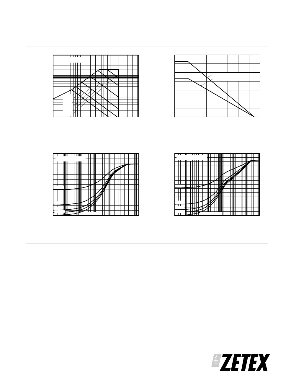
N-CHANNEL CHARACTERISTICS
ZXMD63C02X
100
Refer N ote (a)
10
1
- Drain Current (A)
D
I
0.1
DC
1s
100ms
10ms
1ms
100us
0.1 10 100
1
VDS - Drain-Source Voltage (V)
Safe Operating Area
120
100
80
60
40
20
Thermal Resistance (°C/W)
0.0001 0.1 100
Refer Note (b)
D=0.5
D=0.2
D=0.1
D=0.05
0
Single Pu lse
0.01 100.001 1
Pulse Width (s)
Transient Thermal Impedance
1.4
1.2
1.0
0.8
Refer Note (b)
Refer Note (a)
0.6
0.4
0.2
0
Max Power Dissipation (Watts)
080160
60 14020 40 100 120
T - Temperature (°)
Derating Curve
160
140
120
100
80
60
40
20
Thermal Resistance (°C/W)
0
0.0001 10000.001 0.01 0.1 1 10
D=0.5
D=0.2
D=0.1
D=0.05
Refer N ote (a)
Pulse Width (s)
Single Pulse
100
Transient Thermal Impedance
PROVISIONAL ISSUE A - JUNE 1999
3
Page 4
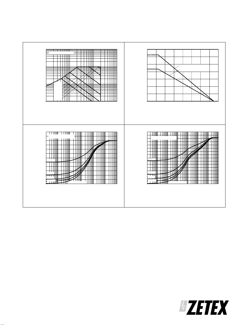
ZXMD63C02X
P-CHANNEL CHARACTERISTICS
100
Refer Note (a)
10
1
ID - Drain Current (A)
0.1
DC
1s
100ms
10ms
1ms
100µs
0.1 10 100
VDS - Drain-Source Voltage (V)
1
Safe Operating Area
120
100
80
60
40
20
Thermal Resistance (°C/W)
0
0.0001 0.1 100
D=0.5
D=0.2
D=0.1
D=0.05
Refer No te (b)
Single Pulse
0.01 100.001 1
Pulse Width (s)
Transient Thermal Impedance
1.4
1.2
1.0
0.8
Refer Note (b)
Refer Note (a)
0.6
0.4
0.2
0
Max Power Dissipation (Watts)
080160
60 14020 40 100 120
T - Temperature (°)
Derating Curve
160
D=0.5
D=0.2
D=0.1
D=0.05
Refer Note (a)
Single Pulse
Pulse Width (s)
100
140
120
100
80
60
40
20
Thermal Resistance (°C/W)
0
0.0001 10000.001 0.01 0.1 1 10
Transient Thermal Impedance
PROVISIONAL ISSUE A - JUNE 1999
4
Page 5

ZXMD63C02X
N-CHANNEL
ELECTRICAL CHARACTERISTICS (at T
PARAMETER SYMBOL MIN. TYP. MAX. UNIT CONDITIONS.
STATIC
Drain-Source Breakdown Voltage V
Zero Gate Voltage Drain Current I
Gate-Body Leakage I
Gate-Source Threshold Voltage V
Static Drain-Source On-State Resistance
(1)
Forward Transconductance (3) g
DYNAMIC (3)
Input Capacitance C
Output Capacitance C
Reverse Transfer Capacitance C
SWITCHING(2) (3)
Turn-On Delay Time t
Rise Time t
Turn-Off Delay Time t
Fall Time t
Total Gate Charge Q
Gate-Source Charge Q
Gate Drain Charge Q
(BR)DSS
DSS
GSS
GS(th)
R
DS(on)
fs
iss
oss
rss
d(on)
r
d(off)
f
g
gs
gd
= 25°C unless otherwise stated).
amb
20 V
1
100 nA
0.7 V
0.130
0.150
µA
Ω
Ω
=250µA, VGS=0V
I
D
VDS=20V, VGS=0V
=± 12V, VDS=0V
V
GS
=250µA, VDS= V
I
D
VGS=4.5V, ID=1.7A
=2.7V, ID=0.85A
V
GS
2.6 S VDS=10V,ID=0.85A
350 pF
=15 V, VGS=0V,
V
120 pF
DS
f=1MHz
50 pF
3.4 ns
8.1 ns
13.5 ns
9.1 ns
V
=10V, ID=1.7A
DD
R
=6.0Ω, RD=5.7Ω
G
(Refer to test
circuit)
6nC
=16V,VGS=4.5V,
V
0.65 nC
2.5 nC
DS
=1.7A
I
D
(Refer to test
circuit)
GS
SOURCE-DRAIN DIODE
Diode Forward Voltage (1) V
Reverse Recovery Time (3) t
Reverse Recovery Charge(3) Q
SD
rr
rr
15.0 ns Tj=25°C, IF=1.7A,
5.9 nC
(1) Measured under pulsed conditions. Width=300µs. Duty cycle ≤2% .
(2) Switching characteristics are independent of operating junction temperature.
(3) For design aid only, not subject to production testing.
PROVISIONAL ISSUE A - JUNE 1999
5
0.95 V Tj=25°C, IS=1.7A,
=0V
V
GS
di/dt= 100A/µs
Page 6

ZXMD63C02X
N-CHANNEL TYPICAL CHARACTERISTICS
100
+25°C
3.5V4V4.5V5V
VGS
10
1
- Drain Current (A)
D
I
0.1
0.1 100
110
3V
2.5V
2V
VDS - Drain-Source Voltage (V)
Output Characteristics
100
VDS=10 V
10
T=150°C
T=25°C
1
- Drain Current (A)
D
I
0.1
1.5 323.5
12.54
VGS - Gate-Source Voltage (V)
Typical Transfer Characteristics
100
+150°C
10
1
- Drain Current (A)
D
I
0.1
0.1 10 100
1
3.5V4V5V4.5V
VDS - Drain-Source Voltage (V)
Output Characteristics
1.8
1.6
GS(th)
1.4
1.2
and V
1.0
DS(on)
0.8
0.6
0.4
0.2
Normalised R
Tj - Junction Temperature (°C)
RDS(on)
VGS(th)
Normalised RDS(on) and VGS(th)
v Temperature
VGS
3V
2.5V
2V
VGS=4. 5V
VGS=VDS
ID=250u A
1500-50 100
ID=1.7A
20050-100
10
1
VGS=3V
VGS=5V
0.1
0.01
0.1 10 100 0.2 0.8 1.4
- Drain-Source On-Resistance (Ω)
1
ID - Drain Current (A)
On-Resistance v Drain Current
DS(on)
R
PROVISIONAL ISSUE A - JUNE 1999
100
10
1
T=150°C
- Reverse Drain Current (A)
SD
I
0.1
0.4 1.00.6 1.2
T=25°C
VSD - Source-Drain Voltage (V)
Source-Drain Diode Forward Voltage
6
Page 7

N-CHANNEL CHARACTERISTICS
ZXMD63C02X
800
700
600
500
400
300
200
C - Capacitance (pF)
100
0
0.1 10 100 0 3 6
1
Ciss
Coss
Crss
Vgs=0V
f=1Mhz
VDS- Drain Source Voltage (V)
Capacitance v Drain-Source Voltage
5
ID=1.7A
4
VDS=16V
- Gate-Source Voltage (V)
GS
V
3
2
1
0
12 45
Q -Charge (nC)
Gate-Source Voltage v Gate Charge
Basic Gate Charge Waveform
Switching Time Waveforms
PROVISIONAL ISSUE A - JUNE 1999
Gate Charge Test Circuit
Switching Time Test Circuit
7
Page 8

ZXMD63C02X
P-CHANNEL
ELECTRICAL CHARACTERISTICS (at T
PARAMETER SYMBOL MIN. TYP. MAX. UNIT CONDITIONS.
STATIC
Drain-Source Breakdown Voltage V
Zero Gate Voltage Drain Current I
Gate-Body Leakage I
Gate-Source Threshold Voltage V
Static Drain-Source On-State Resistance
(1)
Forward Transconductance (3) g
DYNAMIC (3)
Input Capacitance C
Output Capacitance C
Reverse Transfer Capacitance C
SWITCHING(2) (3)
Turn-On Delay Time t
Rise Time t
Turn-Off Delay Time t
Fall Time t
Total Gate Charge Q
Gate-Source Charge Q
Gate Drain Charge Q
(BR)DSS
DSS
GSS
GS(th)
R
DS(on)
fs
iss
oss
rss
d(on)
r
d(off)
f
g
gs
gd
= 25°C unless otherwise stated).
amb
-20 V
-1
±100
-0.7 V
0.27
0.40
µA
nA
Ω
Ω
=-250µA, VGS=0V
I
D
VDS=-20V, VGS=0V
VGS=± 12V, VDS=0V
=-250µA, VDS=
I
D
V
GS
VGS=-4.5V, ID=-1.2A
=-2.7V, ID=-0.6A
V
GS
1.3 S VDS=-10V,ID=-0.6A
290 pF
=-15 V, VGS=0V,
V
120 pF
DS
f=1MHz
50 pF
3.4 ns
9.6 ns
16.4 ns
20.4 ns
V
=-10V, ID=-1.2A
DD
R
=6.0Ω, RD=8.3Ω
G
(Refer to test
circuit)
5.25 nC
=-16V,VGS=-4.5V,
V
1.0 nC
2.25 nC
DS
=-1.2A
I
D
(Refer to test
circuit)
SOURCE-DRAIN DIODE
Diode Forward Voltage (1) V
Reverse Recovery Time (3) t
Reverse Recovery Charge(3) Q
SD
rr
rr
21.7 ns Tj=25°C, IF=-1.2A,
9.6 nC
(1) Measured under pulsed conditions. Width=300µs. Duty cycle ≤2% .
(2) Switching characteristics are independent of operating junction temperature.
(3) For design aid only, not subject to production testing.
PROVISIONAL ISSUE A - JUNE 1999
8
-0.95 V Tj=25°C, IS=-1.2A,
=0V
V
GS
di/dt= 100A/µs
Page 9

P-CHANNEL CHARACTERISTICS
ZXMD63C02X
10
1
- Drain Current (A)
D
-I
0.1
0.1 100
+25 C
5V
4.5V
4V
110
3.5V
3V
2.5V
-VGS
2V
-VDS- Drain-Source Voltage (V)
Output Characteristics
10
VDS=-10V
T=150 C
T=25 C
1
- Drain Current (A)
D
-I
0.1
1.5 323.5
12.54
-VGS - Gate-Source Voltage (V)
Typical Transfer Characteristics
10
+150°C
1
- Drain Current (A)
D
-I
0.1
0.1 10 100
4.5V
5V
4V
1
3.5V
3V
2.5V
-VGS
2V
-VDS- Drain-Source Voltage (V)
Output Characteristics
1.6
GS(th)
1.4
1.2
and V
1.0
DS(on)
0.8
0.6
0.4
4.5
Normalised R
RDS(on)
VGS(th)
VGS=-4.5V
ID=-1.2A
VGS=VDS
ID=-250uA
1500-50 100
20050-100
Tj - Junction Temperature (°C)
Normalised RDS(on) and VGS(th)
v Temperature
10
1
0.1
0.1 10 0.2 0.8 1.4
- Drain-Source On-Resistance (Ω)
-ID - Drain Current (A)
1
On-Resistance v Drain Current
DS(on)
R
PROVISIONAL ISSUE A - JUNE 1999
VGS=-3V
VGS=-5V
10
1
T=150°C
0.1
T=25°C
- Reverse Drain Current (A)
SD
0.01
-I
0.4 1.00.6 1.2
-VSD - Source-Drain Voltage (V)
Source-Drain Diode Forward Voltage
9
Page 10

TYPICAL CHARACTERISTICS
ZXMD63C02X
P-CHANNEL TYPICAL CHARACTERISTICS
700
600
500
400
300
200
C - Capacitance (pF)
100
0
0.1 10 100 0 4 4.5
-VDS- Drain Source Voltage (V)
1
Ciss
Coss
Crss
Vgs=0V
f=1Mhz
Capacitance v Drain-Source Voltage
5
ID=-1.2A
4.5
4
3.5
3
2.5
2
1.5
1
0.5
0
VGS - Gate-Source Voltage (V)
0.5
1231.5
VDS=-16V
Q -Charge (nC)
Gate-Source Voltage v Gate Charge
3.52.5
Basic Gate Charge Waveform
Switching Time Waveforms Switching Time Test Circuit
PROVISIONAL ISSUE A - JUNE 1999
Gate Charge Test Circuit
10
Page 11

ZXMD63C02X
PACKAGE DIMENSIONS
D
5678
E
234
1
e X 6
A1
A
B
Conforms to JEDEC MO-187 Iss A
PAD LAYOUT DETAILS
H
C
DIM Millimetres Inches
MIN MAX MIN MAX
A 1.10 0.043
A1 0.05 0.15 0.002 0.006
B 0.25 0.40 0.010 0.016
C 0.13 0.23 0.005 0.009
D 2.90 3.10 0.114 0.122
θ°
e 0.65 BSC 0.0256 BSC
L
E 2.90 3.10 0.114 0.122
H 4.90 BSC 0.193 BSC
L 0.40 0.70 0.016 0.028
q° 0° 6° 0° 6°
Zetex plc.
Fields New Road, Chadderton, Oldha m, OL9 -8NP, Unit ed Kin gdom .
Telephone: (44)161 622 4422 (Sales), (44)161 622 4444 (General Enquiries)
Fax: (44)161 622 4420
Zetex GmbH Zetex Inc. Zetex (Asia) Ltd. These are supported by
Streitfeldstraße 19 47 Mall Drive, Unit 4 3510 Metroplaza, Tower 2 agents and distributors in
D-81673 München Commack NY 11725 Hing Fong Road, major countries world-wide
Germany USA Kwai Fong, Hong Kong Zetex plc 1999
Telefon: (49) 89 45 49 49 0 Telephone: (516) 543-7100 Telephone:(852) 26100 611
Fax: (49) 89 45 49 49 49 Fax: (516) 864-7630 Fax: (852) 24250 494 Internet:http://www.zetex.com
This publication is issued to provide outline information only which (unless agreed by the Company in writing) may not be used, applied or reproduced for any
purpose or form part of any order or contract or be regarded as a representation relating to the products or services concerned. The Company reserves the
right to alter without notice the specification, design, price or conditions of supply of any product or service.
PROVISIONAL ISSUE A - JUNE 1999
12
 Loading...