

Page 1
ZXGD3003E6
5A(peak) gate driver in SOT23-6
General description
The ZXGD3003E6 is a high-speed non-inverting single MOSFET gate driver capable of driving up to 5A
into a MOSFET or IGBT gate capacitive load from supply voltages up to 40V. With typical propagation
delay times down to 2ns and rise/fall times down to 9ns this device ensures rapid switching of the power
MOSFET or IGBT to minimize power losses and distortion in high current fast switching applications.
The ZXGD3003E6 is inherently rugged to latch-up and shoot-through, and its wide supply voltage range
allows full enhancement to minimize on-losses of the power MOSFET or IGBT.
Its low input voltage requirement and high current gain allows high current driving from low voltage
controller ICs, and the optimized pin-out SOT23-6 package with separate source and sink pins eases
board layout, enabling reduced parasitic inductance and independent control of rise and fall slew rates.
Features
• 40V operating voltage range
• 5 amps peak output current
• Fast switching emitter-follower configuration
• 2ns propagation delay time
• 19ns rise/fall time, 1000pF load
• Low input current requirement
• 1.6A(source)/1.4A(sink) output current from 10mA input
• SOT23-6 package
• Separate source and sink outputs for independent control of rise and fall time
• Optimized pin-out to ease board layout and minimize trace inductance
• No Latch Up
• No shoot through
• Near - Zero quiescent and output leakage current
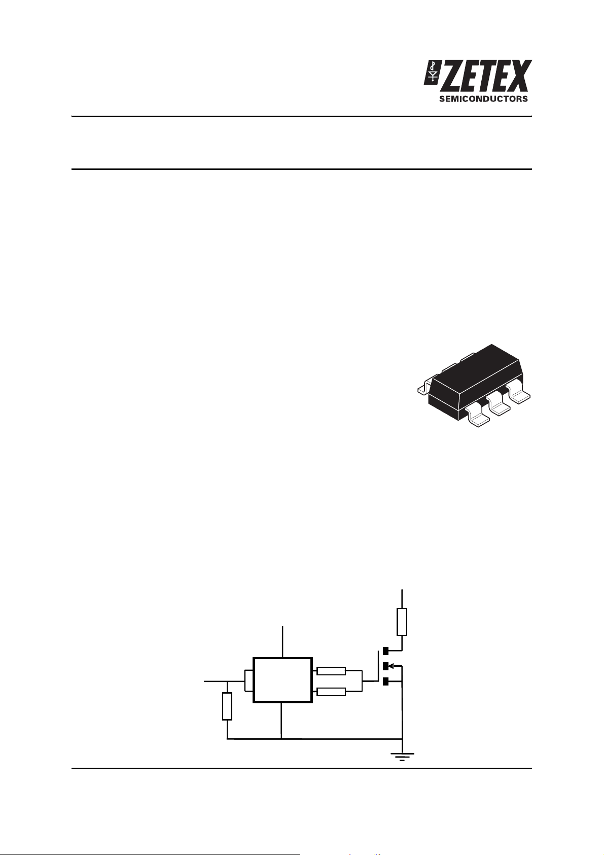
Typical application circuit
V
S
V
CC
V
CC
IN
1
Input
IN
2
ZXGD3003
GND
Issue 2 - October 2007 1 www.zetex.com
© Zetex Semiconductors plc 2007
SOURCE
SINK
Page 2
Applications
Power MOSFET and IGBT Gate Driving in
• Synchronous switch-mode power supplies
• Secondary side synchronous rectification
• Plasma Display Panel power modules
• 1, 2 and 3-phase motor control circuits
• Audio switching amplifier power output stages
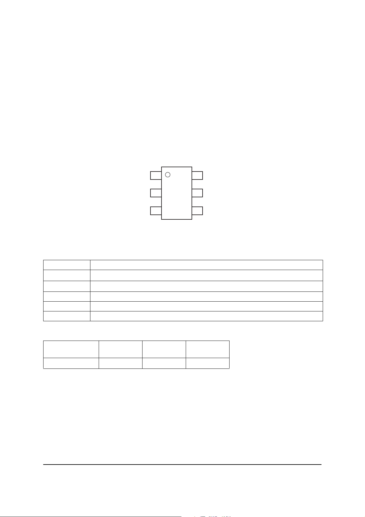
Pin configuration
ZXGD3003E6
V
CC
IN
1
GND
Pin description
Pin Name Pin Function
V
IN
CC
/ IN
1
2
Driver supply
Driver input pins. These are normally connected together by circuit tracks.
GND Ground
SOURCE Source current output.
SINK Sink current output.
Ordering information
Device Reel size
(inches)
Tape width
SOT236
Top view
(mm)
SOURCE
IN
2
SINK
Quantity per
reel
ZXGD3003E6TA 7 8 embossed 3000
Device marking
3003
Issue 2 - October 2007 2 www.zetex.com
© Zetex Semiconductors plc 2007
Page 3
ZXGD3003E6
Absolute maximum ratings
Parameter Symbol Limit Unit
Supply voltage V
Input voltage V
(c)
(c)
IN1
IN1
+ I
+ I
IN2
=10mA
IN2
=25°C
A
=10mA
(a)
(a)(b)
(a)
Peak sink current
Source current @ I
Sink current @ I
Input current
Power dissipation at T
CC
IN
I
(sink)PK
I
(source)
I
(sink)
I
IN1, IIN2
P
D
Linear derating factor 8.8 mW/°C
Operating and storage temperature range T
, T
j
stg
Thermal resistance
Parameter Symbol Value Unit
Junction to ambient
(a)(b)
R
⍜JC
40 V
40 V
5A
1.6 A
1.4 A
1A
1.1 W
-55 to +150
°C
113 °C/W
NOTES:
(a) For a device surface mounted on 25mm x 25mm x 0.6mm FR4 PCB with high coverage of single sided 1oz copper,
in still air conditions.
(b) For device with two active dice running at equal power.
(c) Pulse width <=300us limit repetition rate to comply with maximum junction temperature.
Issue 2 - October 2007 3 www.zetex.com
© Zetex Semiconductors plc 2007
Page 4

ZXGD3003E6
Electrical characteristics (at Tamb = 25°C unless otherwise stated).
Parameter Symbol Min. Typ. Max. Unit Conditions
Output voltage, high V
Output voltage, low V
Source output leakage
current
Sink output leakage
current
Quiescent current I
Source output current I
Sink output current I
Source output current I
Sink output current I
Gate driver
switching times
Gate driver
switching times
OH
OL
I
L(source)
I
L(sink)
Q
(source)
(sink)
(source)PK
(sink)PK
t
d(rise)
t
r
t
d(fall)
t
f
t
d(rise)
t
r
t
d(fall)
t
f
VCC – 0.4 V I
0.4 V I
source
= 1A
sink
= 1A
1 AVCC = 40V,
V
IN1 = VIN2
1 AVCC = 40V,
V
IN1 = VIN2
20 nA VCC = 32V,
V
IN1 = VIN2
11.6 AI
11.4 AI
5AI
5AI
1.8
8.9
1.7
8.9
4
77
4
85
ns
ns
ns
ns
ns
ns
ns
ns
IN1+IIN2
IN1+IIN2
IN1+IIN2
IN1+IIN2
C
=1nF, RL=1⍀,
L
V
=12V, VIN=10V,
CC
=25⍀
R
S
C
=1nF, RL=1⍀,
L
V
=12V, VIN=10V,
CC
=1k⍀
R
S
= 10mA
= 10mA
= 500mA
= 500mA
= 0V
= V
= 0V
CC
Switching time test circuits Timing diagram
Issue 2 - October 2007 4 www.zetex.com
© Zetex Semiconductors plc 2007
Page 5

Typical gate driver characteristics
ZXGD3003E6
Issue 2 - October 2007 5 www.zetex.com
© Zetex Semiconductors plc 2007
Page 6

ZXGD3003E6
Issue 2 - October 2007 6 www.zetex.com
© Zetex Semiconductors plc 2007
Page 7

SOT23-6 Package outline
ZXGD3003E6
0.95
0.037
1.06
0.042
2.2
0.087
0.65
0.026
DIM Millimeters Inches
Min. Max. Min. Max.
A 0.90 1.45 0.0354 0.0570
A1 0.00 0.15 0.00 0.0059
A2 0.90 1.30 0.0354 0.0511
b 0.35 0.50 0.0078 0.0196
C 0.09 0.26 0.0035 0.0102
D 2.70 3.10 0.1062 0.1220
E 2.20 3.20 0.0866 0.1181
E1 1.30 1.80 0.0511 0.0708
L 0.10 0.60 0.0039 0.0236
e 0.95 REF 0.0374 REF
e1 1.90 REF 0.0748 REF
L 0° 30° 0° 30°
Note: Controlling dimensions are in millimeters. Approximate dimensions are provided in inches
mm
inches
Issue 2 - October 2007 7 www.zetex.com
© Zetex Semiconductors plc 2007
Page 8

ZXGD3003E6
Definitions
Product change
Zetex Semiconductors reserves the right to alter, without notice, specifications, design, price or conditions of supply of any product or
service. Customers are solely responsible for obtaining the latest relevant information before placing orders.
Applications disclaimer
The circuits in this design/application note are offered as design ideas. It is the responsibility of the user to ensure that the circuit is fit for
the user’s application and meets with the user’s requirements. No representation or warranty is given and no liability whatsoever is
assumed by Zetex with respect to the accuracy or use of such information, or infringement of patents or other intellectual property rights
arising from such use or otherwise. Zetex does not assume any legal responsibility or will not be held legally liable (whether in contract,
tort (including negligence), breach of statutory duty, restriction or otherwise) for any damages, loss of profit, business, contract,
opportunity or consequential loss in the use of these circuit applications, under any circumstances.
Life support
Zetex products are specifically not authorized for use as critical components in life support devices or systems without the express written
approval of the Chief Executive Officer of Zetex Semiconductors plc. As used herein:
A. Life support devices or systems are devices or systems which:
1. are intended to implant into the body
or
2. support or sustain life and whose failure to perform when properly used in accordance with instructions for use provided in the
labeling can be reasonably expected to result in significant injury to the user.
B. A critical component is any component in a life support device or system whose failure to perform can be reasonably expected to
cause the failure of the life support device or to affect its safety or effectiveness.
Reproduction
The product specifications contained in this publication are issued to provide outline information only which (unless agreed by the
company in writing) may not be used, applied or reproduced for any purpose or form part of any order or contract or be regarded as a
representation relating to the products or services concerned.
Terms and Conditions
All products are sold subjects to Zetex’ terms and conditions of sale, and this disclaimer (save in the event of a conflict between the two
when the terms of the contract shall prevail) according to region, supplied at the time of order acknowledgement.
For the latest information on technology, delivery terms and conditions and prices, please contact your nearest Zetex sales office.
Quality of product
Zetex is an ISO 9001 and TS16949 certified semiconductor manufacturer.
To ensure quality of service and products we strongly advise the purchase of parts directly from Zetex Semiconductors or one of our
regionally authorized distributors. For a complete listing of authorized distributors please visit: www.zetex.com/salesnetwork
Zetex Semiconductors does not warrant or accept any liability whatsoever in respect of any parts purchased through unauthorized sales channels.
ESD (Electrostatic discharge)
Semiconductor devices are susceptible to damage by ESD. Suitable precautions should be taken when handling and transporting devices.
The possible damage to devices depends on the circumstances of the handling and transporting, and the nature of the device. The extent
of damage can vary from immediate functional or parametric malfunction to degradation of function or performance in use over time.
Devices suspected of being affected should be replaced.
Green compliance
Zetex Semiconductors is committed to environmental excellence in all aspects of its operations which includes meeting or exceeding regulatory requirements with respect to the use of hazardous substances. Numerous successful programs have been implemented to reduce
the use of hazardous substances and/or emissions.
All Zetex components are compliant with the RoHS directive, and through this it is supporting its customers in their compliance with
WEEE and ELV directives.
Product status key:
“Preview” Future device intended for production at some point. Samples may be available
“Active” Product status recommended for new designs
“Last time buy (LTB)” Device will be discontinued and last time buy period and delivery is in effect
“Not recommended for new designs”
“Obsolete” Production has been discontinued
Datasheet status key:
“Draft version” This term denotes a very early datasheet version and contains highly provisional information, which
“Provisional version” This term denotes a pre-release datasheet. It provides a clear indication of anticipated performance.
“Issue” This term denotes an issued datasheet containing finalized specifications. However, changes to
Zetex sales offices
Europe
Zetex GmbH
Kustermann-park
Balanstraße 59
D-81541 München
Germany
Telefon: (49) 89 45 49 49 0
Fax: (49) 89 45 49 49 49
europe.sales@zetex.com
© 2007 Published by Zetex Semiconductors plc
Device is still in production to support existing designs and production
may change in any manner without notice.
However, changes to the test conditions and specifications may occur, at any time and without notice.
specifications may occur, at any time and without notice.
Americas
Zetex Inc
700 Veterans Memorial Highway
Hauppauge, NY 11788
USA
Telephone: (1) 631 360 2222
Fax: (1) 631 360 8222
usa.sales@zetex.com
Asia Pacific
Zetex (Asia Ltd)
3701-04 Metroplaza Tower 1
Hing Fong Road, Kwai Fong
Hong Kong
Telephone: (852) 26100 611
Fax: (852) 24250 494
asia.sales@zetex.com
Corporate Headquarters
Zetex Semiconductors plc
Zetex Technology Park, Chadderton
Oldham, OL9 9LL
United Kingdom
Telephone: (44) 161 622 4444
Fax: (44) 161 622 4446
hq@zetex.com
Issue 2 - October 2007 8 www.zetex.com
© Zetex Semiconductors plc 2007
 Loading...