

Page 1
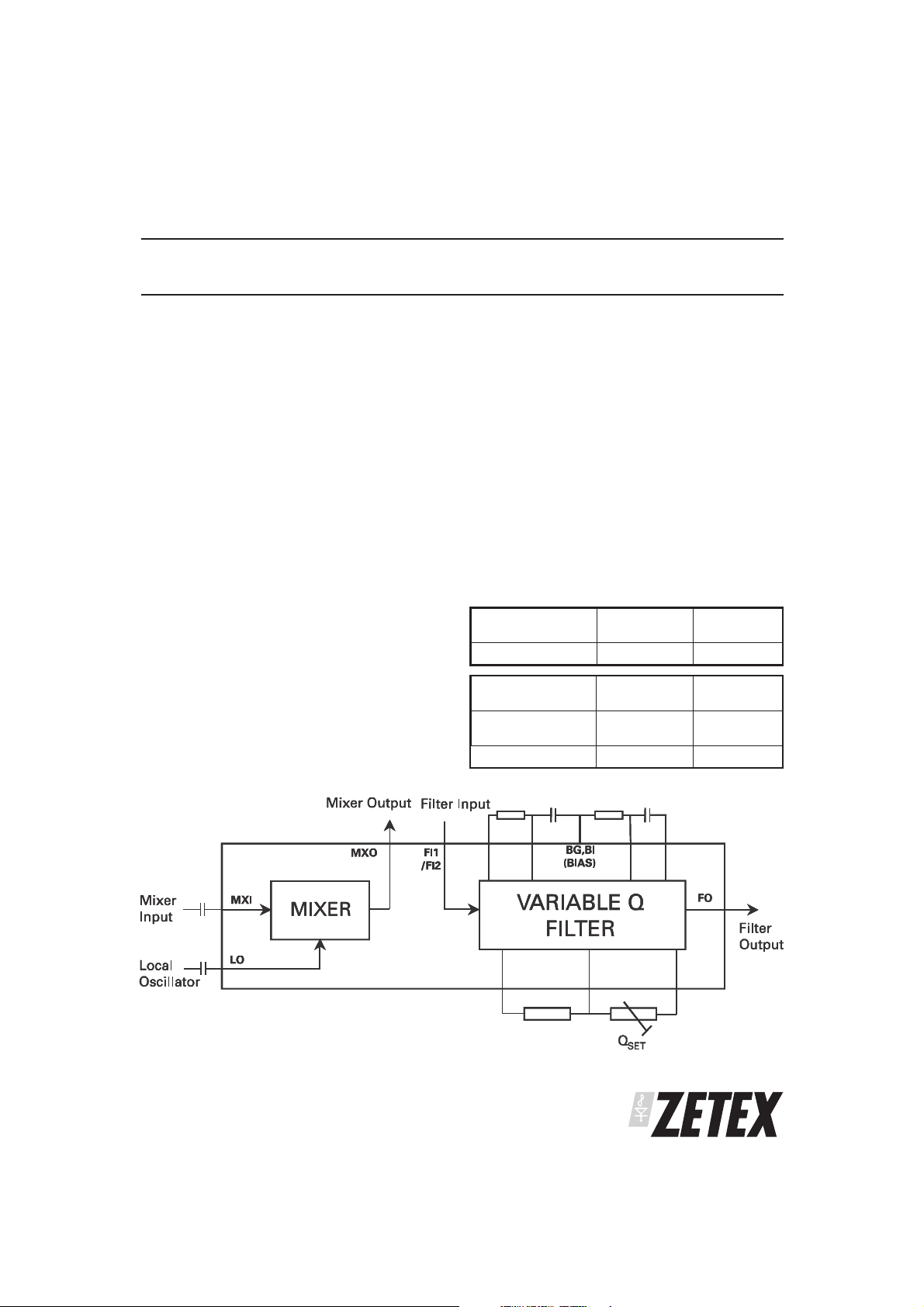
VARIABLE Q FILTER
ZXF36L01
DESCRIPTION
The ZXF36L01 is a versatile analog high Q bandpass
filter. The device contains two sections:
1 Variable Q bandpass filter.
2 Mixer block.
The basic filter section requires 2 resistors and 2
capacitors to set the centre frequency. The filter
operates up to a frequency of 150kHz. Two external
resistors control filter Q Factor. The Q can be varied up
to 50.
The mixer is includedto extend thefrequency range up
to 700kHz and to permit the centre frequency to be
tuned. The local oscillator can be any waveform,
making microprocessor control convenient.
SYSTEM DIAGRAM
APPLICATIONS
Many filter applications including: -
Audio bandpass and notch
•
Micro controlled frequency
•
Adaptive filtering
•
Sonar and Ultrasonic Systems
•
Instrumentation
•
FEATURES AND BENEFITS
Centre Frequency up to 700kHz
•
Tuneable centre frequency
•
Variable Q
•
Low power
•
• Standby mode for improved battery life
ORDERING INFORMATION
PART NUMBER PACKAGE PART
ZXF36L01W24 SO24W ZXF36L01
PART NUMBER CONTAINER INCREMENT
ZXF36L01W24TC Reel 13”
330mm
ZXF36L01W24 Tube 31
MARK
1000
ISSUE 3 - JANUARY 2002
1
Page 2
ZXF36L01
ABSOLUTE MAXIMUM RATINGS
Voltage on any pin 7.0V (relative to Vss)
Operating temperature range 0 to 70°C (de-rated for -40 to 85ºC)
Storage temperature -55 to 125°C
ELECTRICAL CHARACTERISTICS
Test Coνditions: Temperature =25°C, V
GENERAL CHARACTERISTICS
Parameter Conditions Min. Typical Max. Units
Operating current PD=V
Shutdown current PD
IIH (PD)
IIL (PD)
FILTER CHARACTERISTICS
Max. operating frequency 150 kHz
Q usable range 0.5 50
Centre frequency temperature
coefficient
Average Q temperature
coefficient
Voltage noise 1 – 100 kHz 20
Input impedance 30 50
Max. output swing
Output sink current 150
Output source current 150
MIXER CHARACTERISTICS
Max. operating frequency 700 kHz
Maximum signal input 300 mV pk-pk
Maximum Local Oscillator input 100 mV pk-pk
Minimum Local Oscillator input 5 mV pk-pk
Local Oscillator input Impedance 60
=V
VIH =5V (WRT VSS)1.0µA
VIL =0V (WRT VSS) -1.0 µA
Q=30, fo = 1kHz
Note 1
Q=30, fo = 1kHz
Note 2
Output load ≥10 kΩ
= 5.00V, VSS= 0.00V
DD
DD
SS
2.2 3.4 4.5 mA
160 300 µA
10 ppm/°C
0.1 % /°C
nV/√ Hz
kΩ
1.6 V pk-pk
µA
µA
Ω
NOTE 1
Centre frequency temperature coefficient is dominated by the external R & C components. On chip drift is
negligable.
Note 2
Average Q temperature coefficient is dominated by the external R components.
ISSUE 3 - JANUARY 2002
2
Page 3
ZXF36L01
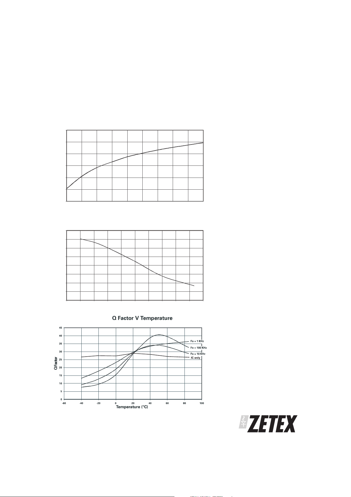
TYPICAL ELECTRICAL CHARACTERISTICS
Test Coνditions:V
TypicalGainatFoVQFactor
50
45
40
35
Gai n (d B)
30
25
20
10 20 30 40 50 60 70 80 90 100
Q Factor
(Fo = 140 KHz)
= 5.00V, VSS= 0.00V
DD
Q Factor V Frequency
32
30
28
26
24
QFactor
22
20
18
16
0 20 40 60 80 100 120 140 160 180 200
Frequency (kHz)
Gain at fo describes the peak gain of
the notch pass filter. This gain is
defined by the value of Q Factor.
The curve shows Q Factor over
frequency for a fixed loop gain
(Rf/Ri).
ISSUE 3 - JANUARY 2002
Components used: 1/8 watt metal
film resistors (+/- 50 ppm). Ceramic
capacitors (+/- 50 ppm).
3
Page 4
ZXF36L01
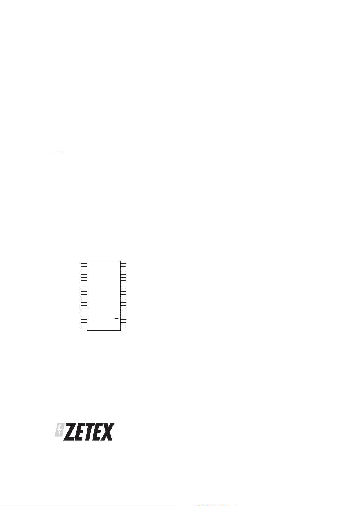
DESCRIPTION OF PIN FUNCTIONS
V
DD
V
SS
BG Bias Generator output. To be decoupled with a 100nF capacitor to V
BI Bias inputs for internal circuitry, both to be connected to BG.
PD
FI1,Fl2 Filter input, FI1 or FI2 depending on filter configuration.
FO Filter output for all configurations.
LO Local Oscillator signal input.
MXI Mixer signal input.
MXO Mixer signal output.
C1, RC1 Phase advance network nodes. Values R and C set centre frequency, fo.
R2, RC2 Phase retard network nodes. Values R and C set centre frequency, fo.
GP1,2,3 Loop gain programming nodes.
CONNECTION DIAGRAM
Positive supply connection (5 volts). Both pins to be connected.
To be decoupled with a 100nF capacitor to V
SS
.
Negative supply connection; system ground (0 volts). Both pins to be connected.
SS
(or external supply referenced to V
Active low. This feature can be used to reduce power consumption for applications that
have a standby mode.
SS
)
.
V
1
SS
FI1
C1
RC1
R2
BI
MXO
RC2
GP1
GP2
GP3
V
SS
V
FI2
MXI
BG
N/C
N/C
N/C
V
DD
FO
LO
BI
PD
DD
ISSUE 3 - JANUARY 2002
4
Page 5

FILTER CONFIGURATIONS AND RESPONSES
q
q
Notch Filter
V
FI2
MXI
BG
N/C
N/C
N/C
V
DD
FO
LO
BI
PD
DD
R=10kΩ
C=100nF
Rf=19.5kΩ
Ri=10kΩ
V
124
SS
FI1
C
R
C
C1
RC1
R2
R
BI
MXO
RC2
GP1
Ri
GP2
GP3
Rf
V
SS
Filter AC Performance
Notch Filter Gain Response
5
0
-5
-10
-15
Gain (dB)
-20
-25
-30
-35
10 100 1000 10000
Fre
uency (Hz)
5V
100nF
5V
100nF
ZXF36L01
100nF
Input Signal
Output Signal
1
f
o
=
2π
RC
f
∝
(/)
QRR
Where R, Ri and Rf ≥10kΩ and C ≥ 50 pF
See “Designing for a Value of Q” for more
details.
i
Notch Filter Phase Response
270
240
210
180
150
Phase ( Degrees)
120
90
10 100 1000 10000
ISSUE 3 - JANUARY 2002
Fre
Typical responses for the circuit with
component values shown in circuit diagram.
uency (Hz)
5
Page 6

ZXF36L01
q
FILTER CONFIGURATIONS AND RESPONSES (continued)
5V
Input Signal
100nF
C
R
R
C
R=10kΩ
C=100nF
Ri
Rf
Rf=19.5kΩ
Ri=10kΩ
Filter AC Performance
Notch Pass Filter Gain Response
Notch Pass Filter Gain Response
30
30
25
25
20
20
15
15
10
10
Gain (dB)
Gain (dB)
5
5
0
0
-5
-5
10 100 1000 10000
10 100 1000 10000
Frequency (H z)
Frequency (H z)
124
V
SS
FI1
C1
RC1
R2
BI
MXO
RC2
GP1
GP2
GP3
V
SS
V
FI2
MXI
LO
BG
N/C
N/C
N/C
V
DD
FO
PD
Output Signal
BI
100nF
5V
DD
100nF
f
o
=
QRR
Where R, Ri and Rf ≥10kΩ and C ≥ 50 pF
See “Designing for a Value of Q” for more
details.
1
2π
RC
fi
∝
(/)
Notch Pass Filter Phase Response
-90
-120
-150
-180
-210
Phase (Degrees )
-240
-270
10 100 1000 10000
Fre
uency (Hz)
Typical responses for the circuit with
component values shown in circuit diagram.
ISSUE 3 - JANUARY 2002
6
Page 7

FILTER CONFIGURATIONS AND RESPONSES (continued)
Notch Filter (with attenuating skirts)
5V
V
FI2
MXI
LO
N/C
N/C
N/C
V
FO
BG
DD
BI
PD
DD
5V
R=10kΩ
C=100nF
Input Signal
100nF
124
V
SS
C
R
C
FI1
C1
RC1
R2
R
BI
MXO
RC2
GP1
Ri
GP2
GP3
Rf
V
SS
Rf=19.5kΩ
Ri=10kΩ
Filter AC Performance
Notch Pass Filter 2 Gain Response
30
20
10
0
Gain (dB)
-10
-20
-30
1 10 100 1000 10000
Frequency (Hz)
Notch Pass Filter 2 Phase Response
120
90
60
30
0
-30
Phas e (Degrees)
-60
-90
-120
1 10 100 1000 10000
Frequency (Hz)
f
o
=
QRR
Where R, Ri and Rf ≥10kΩ and C ≥ 50 pF
See “Designing for a Value of Q” for more
details.
The skirt ‘roll off’ away from the peak is
-20dB/decade regardless of chosen Q.
Typical responses for the circuit with
component values shown in circuit diagram.
Output Signal
100nF
100nF
1
2π
RC
fi
∝
(/)
ZXF36L01
ISSUE 3 - JANUARY 2002
7
Page 8

ZXF36L01
DESIGNING FOR A VALUE OF Q
As mentioned on the configuration pages, there is a
proportional, but non-linear relationship between the
ratio of Rf and Ri, and Q.
These resistors define the gain of an inverting amplifier
that determinesthe peak value gainand therefore the Q
of the filter,Q is defined as:
f
Q
=
−3
This value of required gain is critical. As the maximum
value of Q is approached, too much gain will cause the
filter to oscillate at the centre frequency, fo. A small
reduction of gain will cause the value of Q to fall
significantly. Therefore, for high values of Q or tight
tolerances of lower values of Q, the resistor ratio must
be trimmed as shown.
Frequency dependant effects must be accounted for in
determining the appropriate gain. As the frequency
increases because of internal phase shift effects the
effective circuit gainreduces andthus Q Factorreduces.
The frequency effect is not a problem for circuits where
the fo remains constant, as the phase shifts are
accounted forpermanently. For designs where Q ishigh
and fo is to be ‘swept’, care must be taken that a gain
appropriate at the highest frequency does not cause
oscillation at the lowest.
O
dB Bandwidth
2k
10k
22k
Pin 11Pin 9
Pin 10
Suggestion for gain setting component values.
Below are some typical values of gain required for
several example conditions:
Example1
fo = 48kHz, R = 10kΩ, C = 320pF
Example2
fo = 140kHz, R = 10kΩ, C = 100pF
It can be seen from these examples that the higher Q
example actually has a lower invertingamplifier gain.
As mentioned before, the frequency will affect the
value of gain. The Q Factor v Frequency graph
illustrates this effect.
These examples show that the gain required is
nominally 2. For the specified range of Q: 0.5 to 50
(values up to250 areobtainable), thegain valuesvary
from 1.9 to 2.5 correspondingly.
Due to internal gain errors, when the absolute value
of Q is increased, the device to device variation in Q
will also increase.
Q=60, Rf/Ri = 36.6kΩ / 18 kΩ => 2.033
Q=15, Rf/Ri = 37kΩ / 18kΩ => 2.055
This diagram shows the exponential relationship between gain and Q Factor. (fo = 140 kHz)
ISSUE 3 - JANUARY 2002
8
Page 9

ZXF36L01
FILTERING HIGHER FREQUENCIES USING
THE MIXER
Frequencies above 150 kHz cannot be filtered directly;
the mixerenables thenotch pass filter tofunction up to
700kHz.
The signal to be filtered is mixed with another
frequency (local oscillator), chosen so that the
difference (intermediate) frequency equals the filter’s
centre frequency, fo. The local oscillator signal
waveform can be of any shape (sine, square, etc.) but
must be approximately 50% duty cycle.
Example
Input frequency = 300 kHz, Local Oscillator (LO)
frequency = 250 kHz,
Output (IF) Frequency = 50 kHz.
If the bandwidthof the50 kHzfilter were 1 kHz, the filter’s Q
factor would be:
50/1 = 50.
The bandwidth of the filter is still 1 kHz when 300 kHz is
applied to the mixer’s input, but now the Q factor is:
300/1 = 300.
The mixer provides a Q factor improvement equal to the
ratio of the input frequencyand the intermediate frequency.
The effective centre frequency can also be externally
controlled by changing the LO frequency. This allows
frequency tuning, trimming or sweeping while employing
fixed resistors and capacitors for the filter.
As the LO signal canbe a squarewave, this allows‘fo’ to be
controlled using a microcontroller or microprocessor.
MIXER CONFIGURATION WITH NOTCH PASS FILTER
(with attenuating skirts)
The mixer can only be used with this filter configuration, as
the other types have 0dB stop bands. The mixer output
‘MXO’ becomes the input of the filter.
As the gain of the notch filter changes with Q, the output of
the mixer must be attenuated by some factor (VR
will prevent the filter from being overdriven and allows the
Atten
). This
user to set the required output level.
Note: As the local oscillator input, LO has a low input
impedance (60 Ω), it will often be necessary to increase it
for driving circuitry. As the input voltage required is low
(around 5 mV pk-pk min.), a series resistor ‘R
’ can be
Mixer
inserted. A value of 1 kΩ per 100mV (pk) oscillator signal
input will be suitable.
R
C
ISSUE 3 - JANUARY 2002
5V
V
124
SS
VR
Atten
C
R
Ri
Rf
FI1
C1
RC1
R2
BI
MXO
RC2
GP1
GP2
GP3
V
SS
V
FI2
MXI
LO
BI
BG
N/C
N/C
N/C
V
DD
FO
PD
100nF
R
Mixer
100nF
5V
DD
100nF
Output Signal
Input Signal
100nF
Oscillator Input (LO)
9
Page 10

ZXF36L01
Application Note
An assembled evaluation PCB is available from Zetex Plc, part code: ZXF36L01-EVB. It provides a fast and easy way of
testing the filter configurations mentioned in this datasheet. This board is configured for 10kHz operation.
J1 - J5
1
C1
2
INPUT
100n
3
4
5
VR2
100k
10k
VR1
2k
R
R
10k
1.5nF
I
C
R
22k
C
1.5nF
R
10k
F
1
2
3
4
5
6
7
8
9
10
11
12
ZXF36L01
V
SS
FI1
C1
RC1
R2
BI
MXO
RC2
GP1
GP2
GP3
V
SS
V
FI2
FO
MXI
LO
BG
NC
NC
NC
PD
V
C2
DD
24
23
22
21
20
BI
19
18
17
16
15
14
13
DD
100n
C4
100n
C3
100n
C5
100n
R
MIX
1k
J612
3
+5VINPUT GND
OUTPUT
OUTPUT GND
OSC. INPUT
OSC. GND
POWER GND
JUMPER SETTINGS
NOTCH FILTER
NOTCH PASS FILTER
WITH 0dB STOPBAND
NOTCH PASS FILTER 2
WI TH AT TEN UATI NG
SKIRTS
MIXER CONFIGURATION
WITH NOTCH
PASS FI LTE R 2
NORMAL OPERATION
POWER DOWN
1
2
INPUT IS FI2
3
FEEDBACK FO TO FI1
4
5
1
2
INPUT IS FI1
3
FEEDBACK FI2 TO FI1
4
5
1
2
INPUT IS FI1
3
NO EXTERNAL FEEDBACK
4
5
1
2
INPUT IS MXI
3
MIXED SIGNAL MXO TO FI1
4
NO EXTERNAL FEEDBACK
5
J612
3
J612
3
ISSUE 3 - JANUARY 2002
10
Page 11

Evaluation
An evaluation board (ZXF36L01-EVB) is available to assist with in-system
or stand-alone performance evaluation. The board can be set, by simple
jumper links, to perform any of the filter characteristic responses. The
mixer can beselected inconjunction with the notchpass filter2 functions.
Evaluation boards can be purchased from our catalogue distributors.
Digi-Key North America (www.digikey.com)
Tel:1-800344-4539
Europe - Farnell (www.farnell.com)
Tel:44-113-263-6311
ZXF36L01
ISSUE 3 - JANUARY 2002
11
Page 12

ZXF36L01
PACKAGE DIMENSION
DIM Millimetres Inches
Min Max Min Max
A 15.20 15.40 0.598 0.606
B 1.27 – 0.05 –
C 0.66 – 0.026 –
D 0.36 0.46 0.014 0.018
E 7.40 7.60 0.291 0.299
F 2.44 2.64 0.096 0.104
G 0.10 0.30 0.004 0.012
H 0°7°0°7°
I 0.23 0.28 0.009 0.011
J 10.11 10.51 0.398 0.414
K 0°8°0°8°
L 0.51 1.01 0.02 0.04
R 0.63 0.89 0.025 0.035
a 7°BSC 7°BSC
PACKAGE OUTLINE
SOIC 24 LEAD
© Zetex plc 2001
Zetex plc
Fields New Road
Chadderton
Oldham, OL9 8NP
United Kingdom
Telephone (44) 161 622 4422
Fax: (44) 161 622 4420
These offices are supported by agents and distributors in major countries world-wide.
This publicationis issued toprovide outline informationonly which (unlessagreed by theCompany in writing)may not be used,applied orreproduced
for any purposeor form partof any orderor contract orbe regarded asa representation relatingto the productsor services concerned. The Company
reserves the right to alter without notice the specification, design, price or conditions of supply of any product or service.
For the latest product information, log on to
Zetex GmbH
Streitfeldstraße 19
D-81673 München
Germany
Telefon: (49) 89 45 49 49 0
Fax: (49) 89 45 49 49 49
www.zetex.com
Zetex Inc
700 Veterans Memorial Hwy
Hauppauge, NY11788
USA
Telephone: (631) 360 2222
Fax: (631) 360 8222
Zetex (Asia) Ltd
3701-04 Metroplaza, Tower 1
Hing Fong Road
Kwai Fong
Hong Kong
Telephone: (852) 26100 611
Fax: (852) 24250 494
ISSUE 3 - JANUARY 2002
12
 Loading...