

Page 1
ISSUE 3 - FEBRUARY 2001
ZXCM209
ZXCM210
DESCRIPTION
The ZXCM209/210 are three terminal supervisory
circuits used to monitor the power supplies in
microprocessor and digital systems. They provide a
high performance economical solution when used
with 5V, 3V or lower powered circuits. Reset
thresholds suitable for operation with a variety of
supply voltages are available.
These devices provide a reset signal whenever the
supply voltage falls below a preset threshold, keeping
it asserted for a minimum delay period of 140ms after
the supply has risen above the reset level. The
ZXCM209 has an active-low RESET output (which is
guaranteed to be inthe correct state for suppliesdown
to 1V), while the ZXCM210 has an active-high RESET
output.
The reset comparator hasinbuilthysteresis to prevent
erratic operation and is designed to ignore supply
transients. Low supply current (typically 2µA) makes
the ZXCM209/210 devices ideal for use in portable
equipment. They are available in a 3-pin SOT23
surface mount package with an industry standard
pinout.
FEATURES
•
Enhanced alternative to MAX809/810 and similar
parts
•
Precision monitoring of 5V, 3.3V, 3V power
supply voltages
•
1% threshold tolerance
•
2µA typical supply current
•
140ms minimum power on reset pulse width
•
Alternative minimum pulse widths available,
contact your local sales office for availability
•
RESET LOW Output (ZXCM209)
•
RESET HIGH Output (ZXCM210)
•
Power supply transient immunity
•
No latch up
•
No external components
•
3-Pin SOT23 package
APPLICATIONS
•
Computer systems
•
Controllers
•
Instrumentation
•
Microprocessor power monitoring
•
Microcontroller power monitoring
•
Power supplies
•
Portable/Battery-powered equipment
•
Automotive
VERY LOW POWER MICROPROCESSOR RESET DEVICES
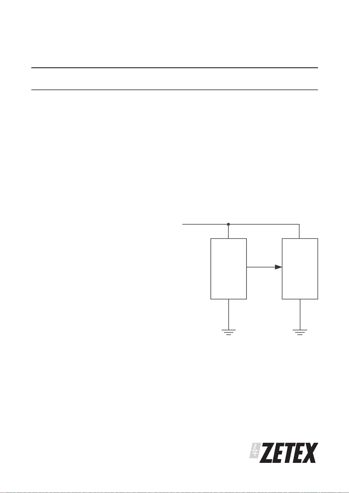
APPLICATION CIRCUIT
v
cc
ZXCM
Reset
Output
Gnd
v
cc
v
cc
Micro
Reset
Input
Gnd
1
Page 2
ZXCM209
ZXCM210
ABSOLUTE MAXIMUM RATINGS
Terminal Voltage with respect to G
ND
V
CC
-0.3V to 7.0V
RESET, RESET
-0.3V to (VCC+ 0.3V)
Input Current, V
CC
20mA
Output Current 20mA
Rate of Rise, V
CC
250V/µs
Continuous Power Dissipation 500mW
Operating Temperature Range -55°C to +125°C
Storage Temperature Range -65°C to +150°C
Stresses beyond those listed under “Absolute Maximum Ratings” may cause permanent damage to the device.
These are stress ratings only, and functional operation of the device at these or any other conditions beyond
those indicated in the operational sections of the specifications is not implied. Exposure to absolute maximum
conditions for extended periods may affect device reliability.
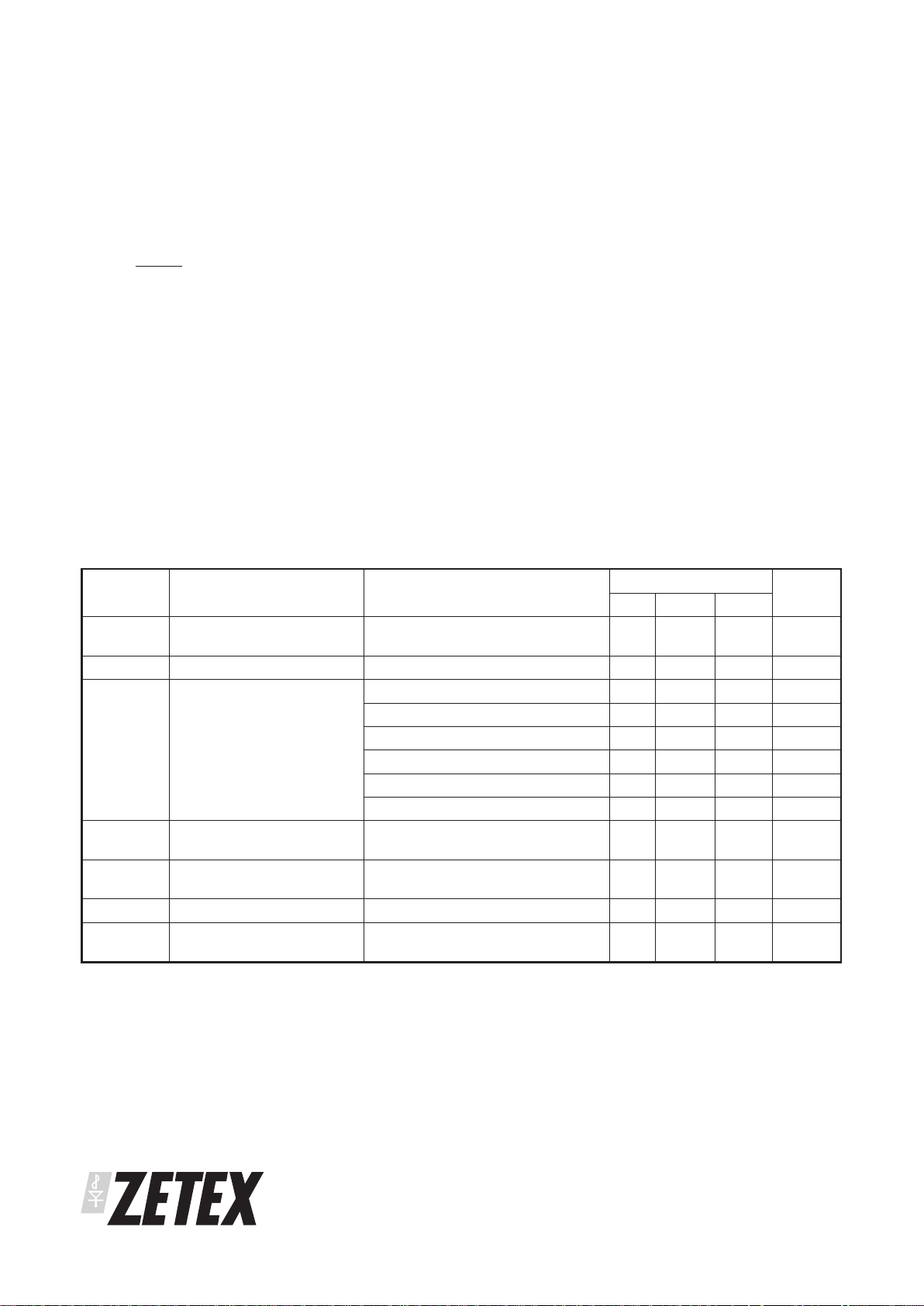
ELECTRICAL CHARACTERISTICS
TEST CONDITIONS (unless otherwise stated) V
CC
= full range, TA= -55°C to +125°C
SYMBOL PARAMETER CONDITIONS LIMITS UNITS
MIN TYP MAX
V
R
VCCRange TA=0° to 70°C
T
A
=-55° to 125°C
1.0
1.2
5.5
5.5
V
V
I
CC
Supply Current 2 5
µA
V
TH
Reset Threshold Suffix L; TA=25°C 4.58 4.63 4.68 V
Suffix M; T
A
=25°C 4.34 4.38 4.42 V
Suffix J; T
A
=25°C 3.96 4.00 4.04 V
Suffix T; T
A
=25°C 3.05 3.08 3.11 V
Suffix S; T
A
=25°C 2.90 2.93 2.96 V
Suffix R; T
A
=25°C 2.60 2.63 2.66 V
V
THT
Reset Threshold
Tolerance
TA=25°C
T
A
=-55° to 125°C
1
5
%
%
∆V
TH
/°C
Reset Threshold Temp.
Coefficient
50 ppm/°C
V
D
VCCto Reset Delay 30
µs
V
TO
Reset Active Timeout
Period
140 560 ms
22
ISSUE 3 - FEBUARY 2001
Page 3
ISSUE 3 - FEBRUARY 2001
ZXCM209
ZXCM210
ELECTRICAL CHARACTERISTICS ZXCM209
TEST CONDITIONS (unless otherwise stated) V
CC
= full range, TA= -55°C to +125°C
SYMBOL PARAMETER CONDITIONS LIMITS UNITS
MIN TYP MAX
V
OL
Reset Output Voltage
Low
V
CC
>1V, IOL=100µA (0 to 85°C)
0.3 V
V
CC
>1.2V, IOL=200µA
0.3 V
V
TH>VCC
>2.5V, IOL=2.7mA
0.4 V
V
OH
Reset Output Voltage
High
V
CC>VTH
max, IOH=1mA
0.8V
cc
V
ELECTRICAL CHARACTERISTICS ZXCM210
TEST CONDITIONS (unless otherwise stated) V
CC
= full range, TA= -55°C to +125°C
SYMBOL PARAMETER CONDITIONS LIMITS UNITS
MIN TYP MAX
V
OL
Reset Output Voltage
Low
V
CC>VTH
max, IOL=2mA
0.3 V
V
CC>VTH
max, IOL=2.7mA
0.4 V
V
OH
Reset Output Voltage
High
V
CC
>1.5V, IOH=150µA
0.8V
cc
V
V
CC>VTH
>2.5V, IOH=1mA
0.8V
cc
V
Note: Device testing is performed at TA=25°C. Device thermal performance is guaranteed by design
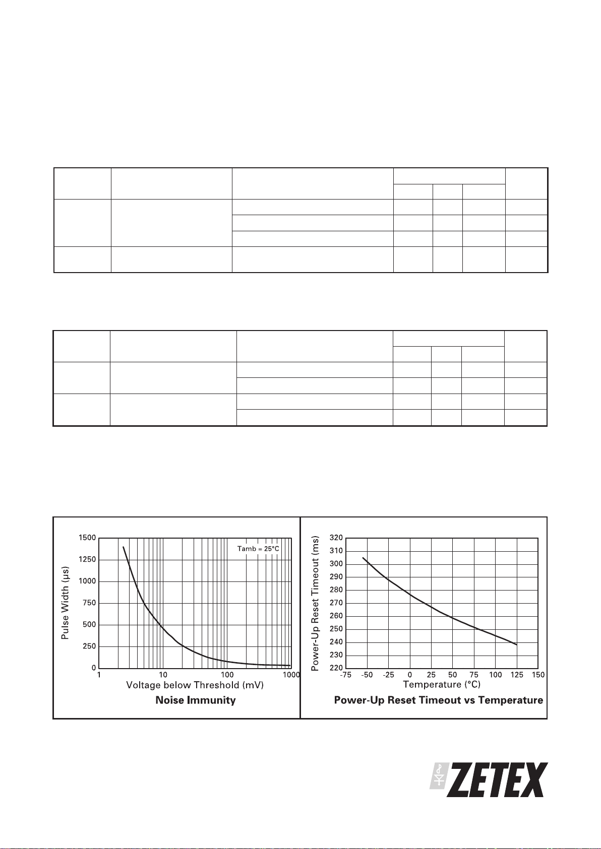
TYPICAL CHARACTERISTICS
3
Page 4

ZXCM209
ZXCM210
ISSUE 3 - FEBUARY 2001
TYPICAL CHARACTERISTICS
4
Page 5

ISSUE 3 - FEBRUARY 2001
ZXCM209
ZXCM210
APPLICATIONS INFORMATION
Negative going V
CC
transients
The ZXCM209/210 are, to a good degree, immune to
short duration negative going supply transients. Under
certain circumstances very brief transients are allowed
without inappropriate false triggering of the reset
circuit. The response to supplytransientsisshown in the
Noise Immunity graph in the typical characteristics. The
graph indicates the typical allowable transient duration
for a specified threshold overdrive such that a reset
pulse is not generated. Addition of a bypass capacitor,
e.g. 0.1µF,as close as possible to the V
CC
pin willprovide
extra transient immunity.
Reset valid down to very low supply voltages
With VCCbetween 0V and 1V the output of the
ZXCM209/210 may be in an undefined state. In many
systems this is inconsequential as the
microprocessor, andother circuits, will be inoperative
with supplies this low. In applications where this is
important, the addition ofan external resistor ensures
that the reset output remains valid for V
CC
< 1V. The
resistor value is non critical: a value of 100kΩ is
recommended. For the ZXCM209 the resistor should
be applied between reset output and ground: for the
ZXCM210 between reset output and V
CC
. Figure 1
shows the connection diagram for the ZXCM devices
in these configurations.
v
cc
ZXCM210
Reset
Output
Gnd
v
cc
Micro
Reset
Input
Gnd
v
cc
100k
v
cc
ZXCM209
Reset
Output
Gnd
v
cc
Micro
Reset
Input
Gnd
v
cc
100k
Figure 1
Circuit for operation of ZXCM with reset valid down to very low supply voltage.
5
Page 6

ZXCM209
ZXCM210
ISSUE 3 - FEBUARY 2001
v
cc
ZXCM
Reset
Output
Gnd
v
cc
Micro
Reset
Input
Gnd
v
cc
4.7kΩ
to other
circuits
Interfacing to µP’s with bidirectional reset I/O
The ZXCM series can be used with microprocessors
havng bidirectional reset pins,suchas Motorola 68HC11
series. The addition of a 4.7k resistor between theZXCM
reset output and the processor input ensures correct
operation of the reset circuit. A buffer to other circuit
components is then required to enable the processor
reset drive to operate correctly. The circuit
configuration is shown in Figure 2.
PIN DESCRIPTION
Pin
Number
Pin Name Pin Function
1V
CC
Supply voltage (+5, +3.3, +3 volts)
2 RESET
(ZXCM209)
RESET
(ZXCM210)
Output remains low while Vcc is below the reset threshold, and for a
minimum 140ms after V
CC
rises above the reset threshold.
Output remains high while V
CC
is below the reset threshold, and for a
minimum 140ms after V
CC
rises above the reset threshold.
3 Gnd Ground
1
2
3
Figure 2
Interfacing to µP’s with bidirectional reset I/O.
6
Page 7

ISSUE 3 - FEBRUARY 2001
ZXCM209
ZXCM210
ORDERING INFORMATION
PART NUMBER TEMPERATURE RANGE PACKAGE RESET OUTPUT
ZXCM209xF -55 to 125°C SOT23 LOW
ZXCM210LF -55 to 125°C SOT23 HIGH
x=Insert appropriate threshold voltage code.
ZXCM209 Threshold voltage codes
PART MARK THRESHOLD
CODE
RESET
THRESHOLD (V)
M22 L 4.63
M23 M 4.38
M24 J 4.00
M25 T 3.08
M26 S 2.93
M27 R 2.63
ZXCM210 Threshold voltage codes
PART MARK THRESHOLD
CODE
RESET
THRESHOLD (V)
M28 L 4.63
The only Reset High variant currently available is the ZXCM210LF. Contact your local Zetex Office for more
details.
7
Page 8

ZXCM209
ZXCM210
ISSUE 3 - FEBUARY 2001
N
PACKAGE DIMENSIONS PAD LAYOUT DETAILS
DIM Millimetres Inches
Min Max Min Max
A 2.67 3.05 0.105 0.120
B 1.20 1.40 0.047 0.055
C – 1.10 – 0.043
D 0.37 0.53 0.0145 0.021
F 0.085 0.15 0.0033 0.0059
G NOM 1.9 NOM 0.075
K 0.01 0.10 0.0004 0.004
L 2.10 2.50 0.0825 0.0985
N
NOM 0.95 NOM 0.037
8
Zetex plc.
Fields New Road, Chadderton, Oldham, OL9-8NP, United Kingdom.
Telephone: (44)161 622 4422 (Sales), (44)161 622 4444 (General Enquiries)
Fax: (44)161 622 4420
Zetex GmbH Zetex Inc. Zetex (Asia) Ltd. These are supported by
Streitfeldstraße 19 47 Mall Drive, Unit 4 3701-04 Metroplaza, Tower 1 agents and distributors in
D-81673 München Commack NY 11725 Hing Fong Road, major countries world-wide
Germany USA Kwai Fong, Hong Kong © Zetex plc 2001
Telefon: (49) 89 45 49 49 0 Telephone: (631) 543-7100 Telephone:(852) 26100 611
Fax: (49) 89 45 49 49 49 Fax: (631) 864-7630 Fax: (852) 24250 494 www.zetex.com
This publication is issued to provide outline information only which (unless agreed by the Company in writing) may not be used, applied or reproduced for
any purpose or form part of any order or contract or be regarded as a representation relating to the products or services concerned. The Company reserves
the right to alter without notice the specification, design, price or conditions of supply of any product or service.
 Loading...