

Page 1
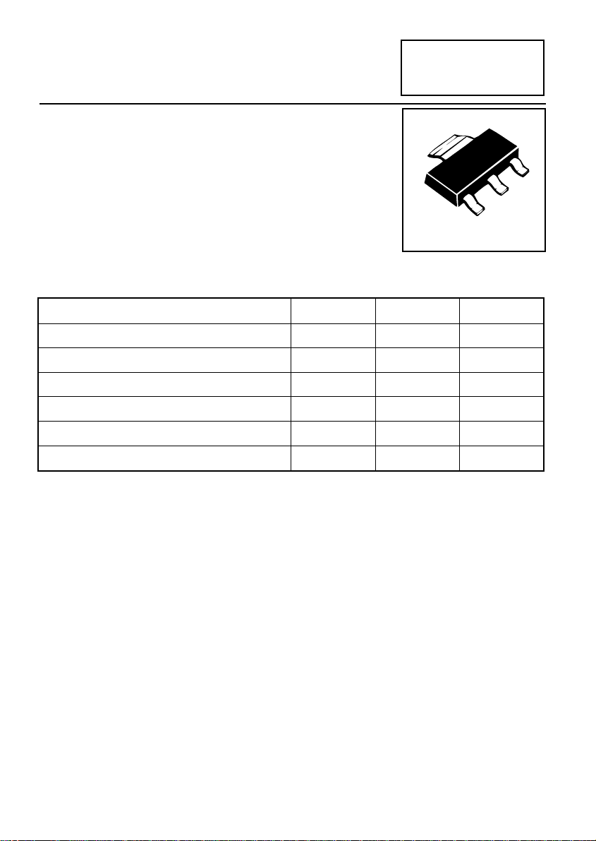
SOT223 P-CHANNEL ENHANCEMENT
ZVP4424G
MODE VERTICAL DMOS FET
ISSUE 2 - OCTOBER 1995
FEATURES
* 240 Volt V
*R
DS(on)
* Low threshold and Fast switching
APPLICATIONS
* Electronic hook switches
* Telecoms and Battery powered equipment
COMPLEMENTARY TYPE - ZVN4424G
PARTMARKING DETAIL - ZVP4424
ABSOLUTE MAXIMUM RATINGS.
PARAMETER SYMBOL VALUE UNIT
DS
= 8.8Ω typical at V
GS
=-3.5V
D
G
S
D
Drain-Source Voltage V
Continuous Drain Current at T
=25°C I
amb
Pulsed Drain Current I
Gate Source Voltage V
Power Dissipation at T
=25°C P
amb
Operating and Storage Temperature Range T
DS
D
DM
GS
tot
j:Tstg
-240 V
-480 mA
-1.0 A
± 40
2.5 W
-55 to +150 °C
V
3 - 438
Page 2
ZVP4424G
ZVP4424G
ELECTRICAL CHARACTERISTICS (at T
= 25°C unless otherwise stated).
amb
PARAMETER SYMBOL MIN. TYP MAX. UNIT CONDITIONS.
Drain-Source Breakdown
BV
Voltage
Gate-Source Threshold
Voltage
Gate-Body Leakage I
Zero Gate Voltage Drain
Current
On-State Drain Current I
Static Drain-Source
On-State Resistance
Forward
Transconductance (1) (2)
Input Capacitance (2) C
Common Source Output
Capacitance (2)
Reverse Transfer
Capacitance (2)
Turn-On Delay Time (2)(3) t
Rise Time (2)(3) t
Turn-Off Delay Time (2)(3) t
Fall Time (2)(3) t
(1) Measured under pulsed conditions. Width=300
(2) Sample test.
V
GS(th)
GSS
I
DSS
D(on)
R
DS(on)
g
fs
iss
C
oss
C
rss
d(on)
r
d(off)
f
(3) Switching times measured with 50
-240 V ID=-1mA, VGS=0V
DSS
-0.7 -1.4 -2.0 V ID=-1mA, VDS= V
100 nA
-10
µA
-100
µA
=± 40V, V
V
GS
V
=-240V, VGS=0V
DS
=-190V, VGS=0V, T=125°C
V
DS
-0.75 -1.0 A VDS=-10V, VGS=-10V
7.1
8.8911
VGS=-10V, ID=-200mA
Ω
V
Ω
GS
=-3.5V, ID=-100mA
125 mS VDS=-10V,ID=-0.2A
100 200 pF
18 25 pF
=-25V, VGS=0V, f=1MHz
V
DS
515pF
815ns
815ns
26 40 ns
V
DD
V
GEN
≈−50V, I
=-10V
20 30 ns
µs. Duty cycle ≤2%
Ω source impedance and <5ns rise time on a pulse generator
Spice parameter data is available upon request for this device
=0V
DS
=-0.25A,
D
GS
300
250
F)
(p
200
ce
n
ta
150
ci
a
p
a
100
C
C-
50
0
-0.01 -1 -10 -100
VDS-Drain Source Voltage (Volts)
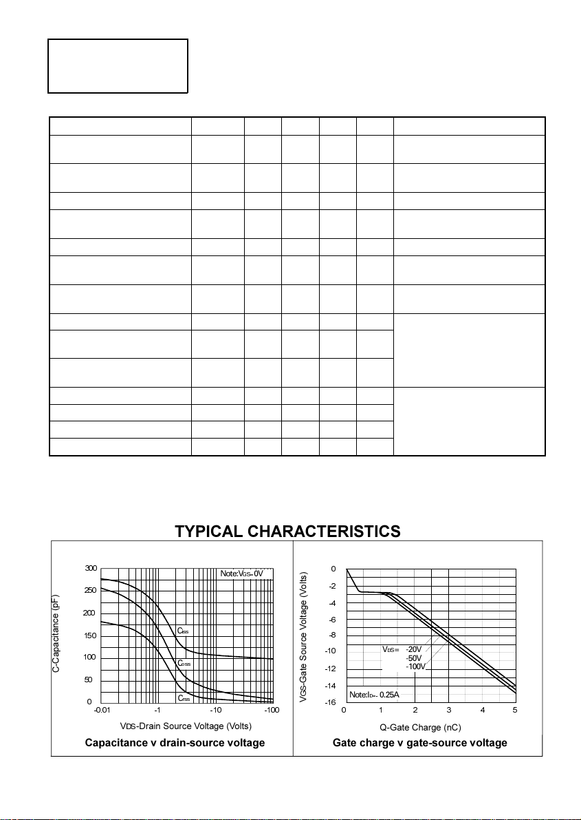
Capacitance v drain-source voltage
TYPICAL CHARACTERISTICS
Note :V
GS=
0V
iss
C
oss
C
rss
C
0
-2
-4
-6
-8
VDS= -20V
D=-
Note :I
0.25A
01 45
Q-Gate Charge (nC)
-Gate Source Voltage (Volts)
S
G
V
-10
-12
-14
-16
Gate charge v gate-source voltage
-50V
-100V
32
Page 3

ZVP4424G
TYPICAL CHARACTERISTICS
-1.2
-1.0
ps)
-0.8
t (Am
-0.6
en
Curr
-0.4
n
ai
r
-0.2
- D
I
0
0-2 -4 -6 -8 -10
300µs Pulsed Test
VDS- Drain Source Voltage (Volts)
Saturation Characteristics
400
300
200
100
-Transconductance (mS)
s
f
g
0
300µs Pulse d Test
V
DS
=-10V
0 -0.2 -0.4 -0.6 -0.8 -1.0
ID- Drain Current (Amps
Transconductance v drain current
-1.2
GS
V
=-10V
-5V
-4V
-3V
-2.5V
-2V
-1.0
ps)
-0.8
nt (Am
-0.6
rre
Cu
-0.4
n
Drai
-0.2
I
0
0-2-4-6-8-10
VGS- Gate Source
VDS=-10V
µ
300
s Pulsed Test
Voltage (Volts)
Transfer Characteristics
400
300
200
100
-Transconductance (mS)
s
f
g
0
0-2-4-6
)
300µs Pulsed Test
V
DS
=-10V
VGS-Gate Source Voltage (Volts)
Transconductance v gate-source voltage
Ω
100
VGS=-2V
10
1
-0.01
RDS(on)-Drain Source On Resistance
I
On-resistance vs Drain Current
-2.5V
-3V
-10V
300µs Pulsed Test
-0.1 -10
D-
Drain Current (Amps)
-1
3 - 4403 - 439
2.4
2.2
2.0
1.8
1.6
1.4
and V
1.2
1.0
R
0.8
0.6
sed
i
0.4
al
0.2
rm
0.0
No
-50
Normalised R
-25 0 25 50 75
Junction Temperature (°C)
DS(on)
and V
GS(th)
GS=
V
-10V
ID=0.2A
V
GS=VDS
ID=-1mA
125
100 150
vs Temperature
 Loading...