

Page 1
ADJUSTABLE PRECISION
ZENER SHUNT REGULATOR
ISSUE 4 – SEPTEMBER 2000
ZR431
DEVICE DESCRIPTION
The ZR431 is a three terminal adjustable
shunt regulator offering excellent
temperature stability and output current
handling capability up to 100mA. The output
voltage may be set to any chosen voltage
between 2.5 and 20 volts by selection of two
external divider resistors.
The devices can be used as a replacement
for zener diodes in many applications
requiring an improvement in zener
performance.
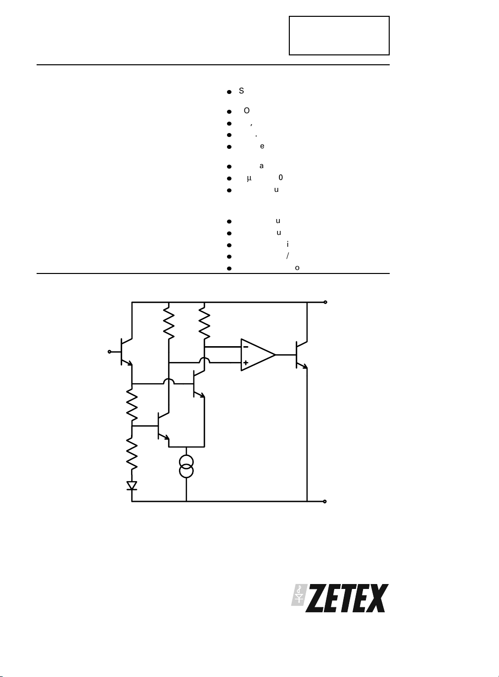
SCHEMATIC DIAGRAM
ref
V
FEATURES
Surface mount SO8, SOT223 and
SOT23 packages
TO92 package
2%, 1 % and 0.5% tolerance
Max. temperature coefficient 55 ppm/°C
Temperature compensated for operation
over the full temperature range
Programmable output voltage
50A to 100mA current sink capability
Low output noise
APPLICATIONS
Shunt regulator
Series regulator
Voltage monitor
Over voltage/ under voltage protection
Switch mode power supplies
V
Z
4-189
78
G
nd
Page 2
ZR431
ABSOLUTE MAXIMUM RATING
Cathode Voltage (VZ) 20V
Cathode Current 150mA
Operating Temperature -40 to 85°C
Storage Temperature -55 to 125°C
Recommended Operating Conditions
Min Max
Cathode Voltage Vref 20V
Cathode Current 50
A 100mA
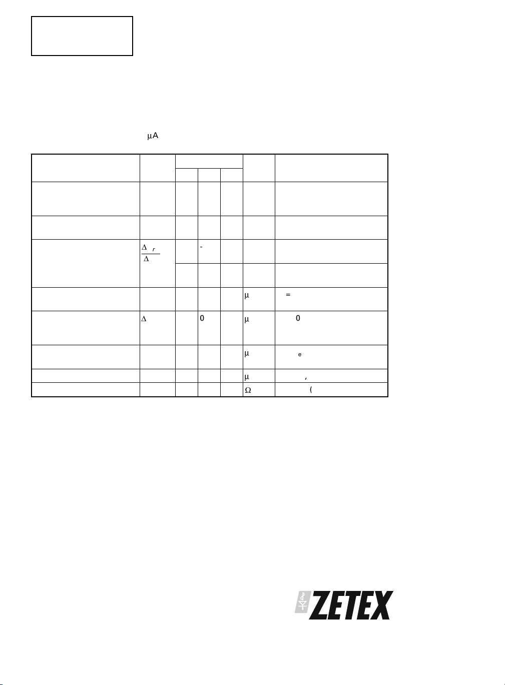
ELECTRICAL CHARACTERISTICS TEST CONDITIONS (Unless otherwise stated):T
ref
V
Z
ref
VALUE
MIN TYP MAX
2.45
2.475
2.489
(1)
0.5%
SYMBOL
V
ref
V
dev
PARAMETER
Reference Voltage 2%
1%
Deviation of Reference Input
Voltage over Temperature
Ratio of the change in
Reference Voltage to the
V
Change in Cathode
Voltage
Reference Input Current I
Deviation of Reference
ref
I
Input Current over
Temperature
Minimum Cathode
I
Zmin
Current for Regulation
Off-state Current I
Dynamic Output Impedance R
(1)
0.5% SOT23 only.
Zoff
Z
For definitions of reference voltage temperature coefficient and dynamic output impedance see
NOTES following DC TEST CIRCUITS
Power Dissipation (T
amb
=25°C,T
SOT23 330mW
TO92 780mW
SOT223 2W
SO8 780mW
UNITS CONDITIONS
2.50
2.50
2.50
2.55
VI
2.525
2.513
=10mA (Fig1), VZ=V
L
8.0 17 mV IL=10mA, VZ=V
Ta=full range (Fig1)
-1.85 -2.7 mV/V VZ from V
=10mA (Fig2)
I
Z
-1.0 -2.0 mV/V V
0.12 1.0
A
from 10V to 20V
Z
=10mA (Fig2)
I
Z
R1=10k, R2=O/C, l
to 10V
ref
(Fig2)
0.04 0.2
35 50
0.1
0.75
R1=10k, R2=O/C, I
A
T
a
V
A
A
Z=Vref
V
Z
VZ=V
=full range (Fig2)
(Fig1)
=20V, V
ref
(Fig1), f=0Hz
ref
=0V (Fig3)
ref
=10mA
L
=150°C)
jmax
=25°C
amb
ref
=10mA
L
4-190
78
Page 3
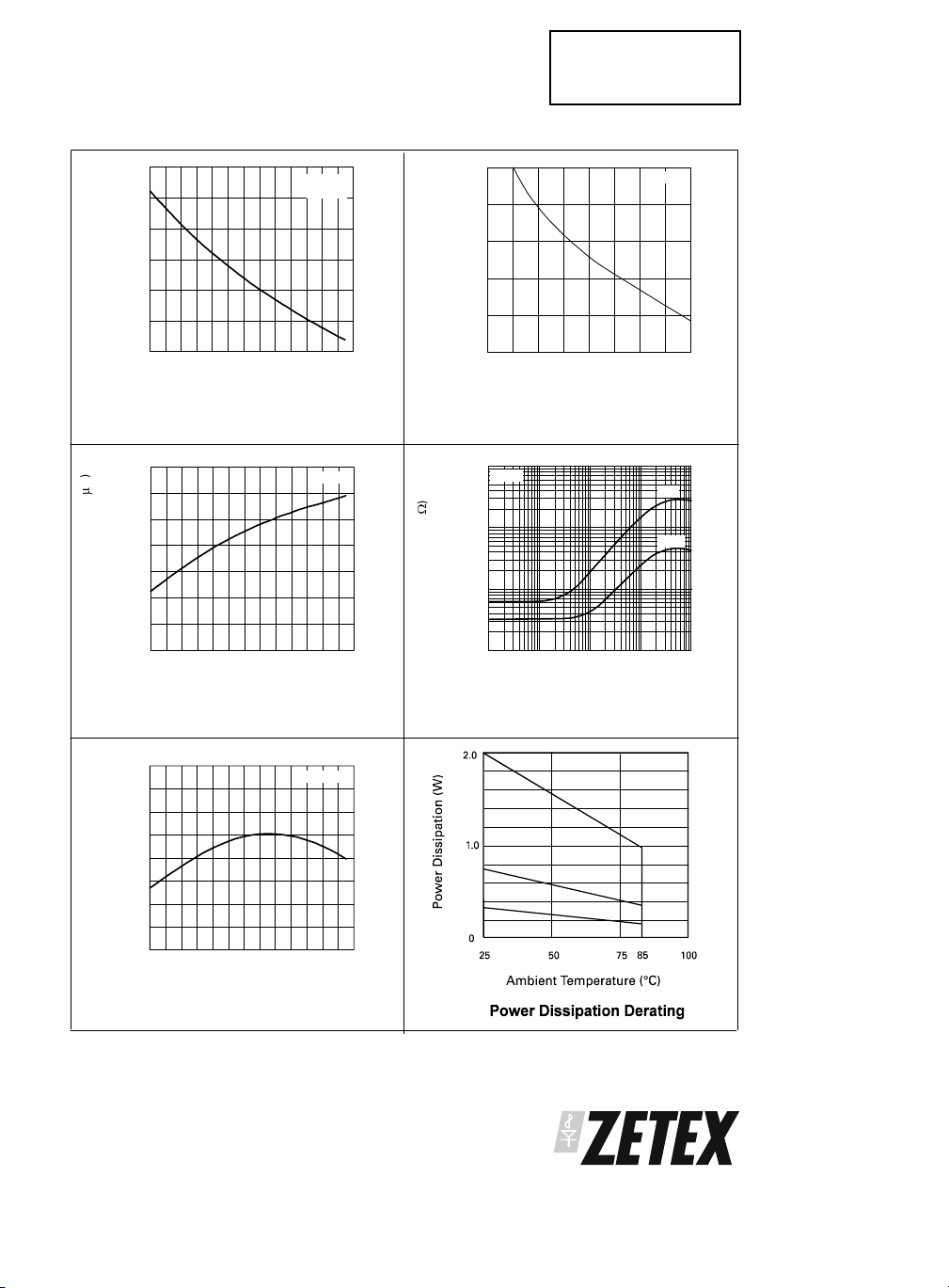
TYPICAL CHARACTERISTICS
160
150
140
130
120
110
Reference Current (nA)
100
-40 0 20 40 60-20 80
Temperature (°C)
Reference Current v Temperature
Vref=VZ
IZ=10mA
0
-5
-10
-15
-20
-25
0
5101520
Change in Reference Output Voltage (mV)
Cathode Voltage (V)
Change in Vrefv Cathode Voltage
ZR431
IZ=10mA
38
A)
36
34
32
30
28
26
Minimum Cathode Current(
24
-40 0 20 40 60-20 80
Temperature (°C)
Cathode Current v Temperature
2.506
2.504
2.502
2.500
2.498
2.496
2.494
Reference Voltage (V)
2.492
2.490
-40 0 20 40 60-20 80
Temperature (°C)
Reference Voltage v Temperature
Vref=VZ
IZ=10mA
100
ref=VZ
V
)
10
1.0
Dynamic Impedance (
0.1
100 1k 10k 100k 1M
Frequency (Hz)
Dynamic Impedance v Frequency
SOT223
SO8/TO92
SOT23
1mA
10mA
4-191
78
Page 4

ZR431
60
40
TYPICAL CHARACTERISTICS
15k
F
9
V
Z
I
Z
230
20
Open Loop Voltage Gain (dB)
0
100 1k 10k 100k 1M
Frequency (Hz)
Gain v Frequency
Voltage Swing (V)
3.0
2.0
1.0
0
5.0
0
Repetitive pulse
Single pulse
0 0.4 0.6 0.8 1.00.2
Tim e (s)
Pulse Response
100
80
60
STABLESTABLE
VZ
INPUT
+
8k25
-
IZ = 10mA, TA = 25°C
Test Circuit for Open Loop Voltage Gain
Input Monitor
Generator
Pulse
TA = 25°C
220
50
Test Circuit for Pulse Response
Input
150
I
Z
10k
V
Z
V
Z
40
20
Cathode Current (mA)
0
100p 1000p
10p
Load Capacitance (F)
Stability Boundary Conditions
0.01
0.11
Vref < VZ < 20, IZ = 10mA, TA = 25°C
Test Circuit for Stability Boundary Conditions
4-192
78
Page 5

APPLICATION CIRCUITS
ZR431
V+ Vout
R1
Vre f
R2
R1
1 +
Vout =
SHUNT REGULATOR
V+
ZSR***
In
Common
Vout = Vref + Vreg
MIN
Vout = 1 +
OUTPUT CONTROL OF A
THREE TERMINAL FIXED REGULATOR
Vref
R2
Vout
Out
R1
Vre f
R2
R1
Vre f
R2
V+ Vout
R1
Vre f
R2
30
0.01µF
R1
1 +
Vref
R2
R1
R2
R1
Vref
R2
Vout =
HIGHER CURRENT SHUNT REGULATOR
V+
Vref
Vout = 1 +
SERIES REGULATOR
Vout
V+
INPUT
= 2.5V
V
TH
SINGLE SUPPLY COMPARATOR
WITH TEMPE RATURE
COMPENSATED THRESHOLD
OUTPUT
V
V
V+
R1A
2V
on
= V+
off
Vref
R2A
R1B
R2B
R1B
1 +
Low limit =
High limit =
OVER VOLTAGE / UNDER VOLTAGE
Vref
R2B
R1A
1 +
Vref
R2A
Vre f
OUTPUT
4-193
78
Page 6

ZR431
DC TEST CIRCUITS
IL
Input
Fig 1 – Test Circuit for Vz=V
Fig 2 – Test Circuit for Vz>V
ref
Input V
ref
NOTES
Deviation of reference input voltage, V
input voltage over the full temperature range.
The average temperature coefficient of the reference input voltage, V
Vmax
Vmin
Vdev = Vmax - Vmin
is defined as the maximum variation of the reference
dev,
V
x 1000000
dev
ppm
°C
V
ref
V
T1T2
ref
The dynamic output impedance, Rz, is defined as:
V
Z
R
Z
I
Z
When the device is programmed with two external
resistors, R1 and R2, (fig 2) , the dynamic output
impedance of the overall circuit, R’, is defined as:
R’
Rz 1
R1
R2
I
Fig 3 – Test Circuit for Off
State current
is defined as:
ref
Z
zoff
4-194
78
Page 7

CONNECTION DIAGRAMS
ZR431
SO8 Package Suffix – N8
Top View
SOT23 Package Suffix – F
Top View
ORDERING INFORMATION
Part Number Package Tol.%Part Mark
SOT223 Package Suffix – G
Top View –
Pin 4 floating or connected to pin 2
TO92 Package Suffix – C
Bottom View
ZR431C01 TO92 1.0 ZR43101
ZR431C TO92 2.0 ZR431
ZR431G01 SOT223 1.0 ZR43101
ZR431G SOT223 2.0 ZR431
ZR431F005 SOT23 0.5 43R
ZR431F01 SOT23 1.0 43B
ZR431F SOT23 2.0 43A
ZR431N801 SO8 1.0 ZR43101
ZR431N8 SO8 2.0 ZR431
4-195
78
 Loading...