

Page 1

FET BIAS CONTROLLER
DRAFT ISSUE A - DECEMBER 2000
DEVICE DESCRIPTION
The ZNBR series of devices are designed to
meet the bias requirements of GaAs and
HEMT FETs commonly used in satellite
receiver LNBs, PMR, cellular telephones etc.
with a minimum of external components
and a V
With the addition of two capacitors and
resistors the devices provide drain voltage
and current control for a number of external
grounded source FETs, generating the
regulated negative rail required for FET gate
biasing whilst operating from a single
supply. This negative bias, at -3 volts, can
also be used to supply other external
circuits.
The ZNBR4000/1 and ZNBR6000/1 contain
four and six bias stages respectively. In
setting drain current the ZNBR4000/1 two
resistors allows individual FET pair control
to different levels, the ZNBR6000/1 two
resistors split control between two and four
FETs. This allows the operating current of
input FETs to be adjusted to minimise noise,
whilst the following FET stages can
separately be adjusted for maximum gain.
The series also offers the choice of drain
voltage to be set for the FETs, the
ZNBR4000/6000 gives 2.2 volts drain whilst
the ZNBR4001/6001 gives 2 volts.
FEATURES
•
•
•
•
•
•
•
•
•
of 3-6V for improved efficiency.
CC
V
of 3-6V for improved efficiency
CC
Provides bias for GaAs and HEMT FETs
Drives up to four or six FETs
Dynamic FET protection
Drain current set by external resistor
Regulated negative rail generator
requires only 2 external capacitors
Choice in drain voltage
Wide supply voltage range
QSOP surface mount package
ZNBR4000ZNBR4000 ZNBR4001
ZNBR6000 ZNBR6001
These devices are unconditionally stable
over the full working temperature with the
FETs in place, subject to the inclusion of the
recommended gate and drain capacitors.
These ensure RF stability and minimal
injected noise.
It is possible to use less than the devices full
complement of FET bias controls, unused
drain and gate connections can be left open
circuit without affecting operation of the
remaining bias circuits.
In order to protect the external FETs the
circuits have been designed to ensure that,
under any conditions including power
up/down transients, the gate drive from the
bias circuits cannot exceed the range -2.5V
to 0.7V. Furthermore if the negative rail
experiences a fault condition, such as
overload or short circuit, the drain supply to
the FETs will shut down avoiding excessive
current flow.
The ZNBR4000/1 and ZNBR6000/1 are
available in QSOP16 and 20 pin packages
respectively for the minimum in devices size.
Device operating temperature is -40 to 70°C
to suit a wide range of environmental
conditions.
APPLICATIONS
Satellite receiver LNBs
•
Private mobile radio (PMR)
•
Cellular telephones
•
1
Page 2
ZNBR4000ZNBR4000 ZNBR4001
ZNBR6000 ZNBR6001
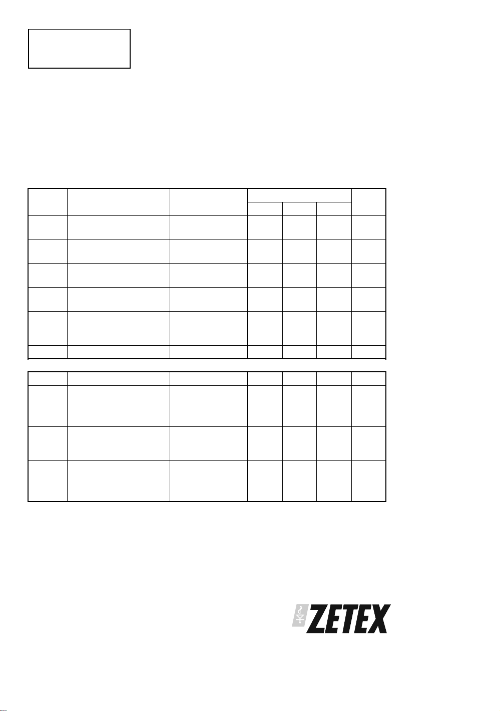
ABSOLUTE MAXIMUM RATINGS
Supply Voltage -0.6V to 15V
Supply Current 100mA
Drain Current (per FET) 0 to 15mA
(set by R
CAL1
and R
CAL2
)
Output Current 100mA
Operating Temperature -40 to 70°C
Storage Temperature -50 to 85°C
Power Dissipation (T
amb
= 25°C)
QSOP16 500mW
QSOP20 650mW
ELECTRICAL CHARACTERISTICS TEST CONDITIONS (Unless otherwise stated):
T
= 25°C,VCC=4V,ID=10mA (R
amb
SYMBOL PARAMETER CONDITIONS
CAL1
=33kΩ;R
CAL2
=33kΩ)
LIMITS
UNITS
Min Typ Max
V
CC
I
CC
I
CC
V
SUB
Supply Voltage ZNBR4000/6000
ZNBR4001/6001
Supply Current
ZNBR4000/1
Supply Current
ZNBR6000/1
Substrate Voltage
(Internally generated)
ID1 to ID4=0
to ID4=10mA
I
D1
ID1 to ID6=0
to ID6=10mA
I
D1
I
= 0
SUB
I
= -200µA
SUB
3.5
3.0
12 V
10
50
15
75
-1.8
-1.8
mA
mA
mA
mA
V
V
Output Noise
E
ND
E
NG
f
O
Drain Voltage
Gate Voltage
Oscillator Freq. 200 350 800 kHz
=4.7nF, CD=10nF
C
G
=4.7nF, CD=10nF
C
G
0.02
0.005
Vpkpk
Vpkpk
DRAIN CHARACTERISTICS
I
D
∆I
∆I
V
∆V
∆V
DV
DT
D
Current 8 1012mA
Current Change
with V
with T
CC
j
VCC=5 to 12V 0.02 %/V
Tj=-40 to +70°C 0.05 %/°C
Voltage
ZNBR4000, ZNGB6000
ZNBR4001, ZNBR6001
2
1.8
2.2
2
2.4
2.2
Voltage Change
DV
DT
with V
with T
CC
j
VCC= 5 to 12V 0.5 %/V
Tj = -40 to +70°C 50 ppm
V
V
2
Page 3
ZNBR4000ZNBR4000 ZNBR4001
ZNBR6000 ZNBR6001
SYMBOL PARAMETER CONDITIONS
LIMITS
UNITS
Min Typ Max
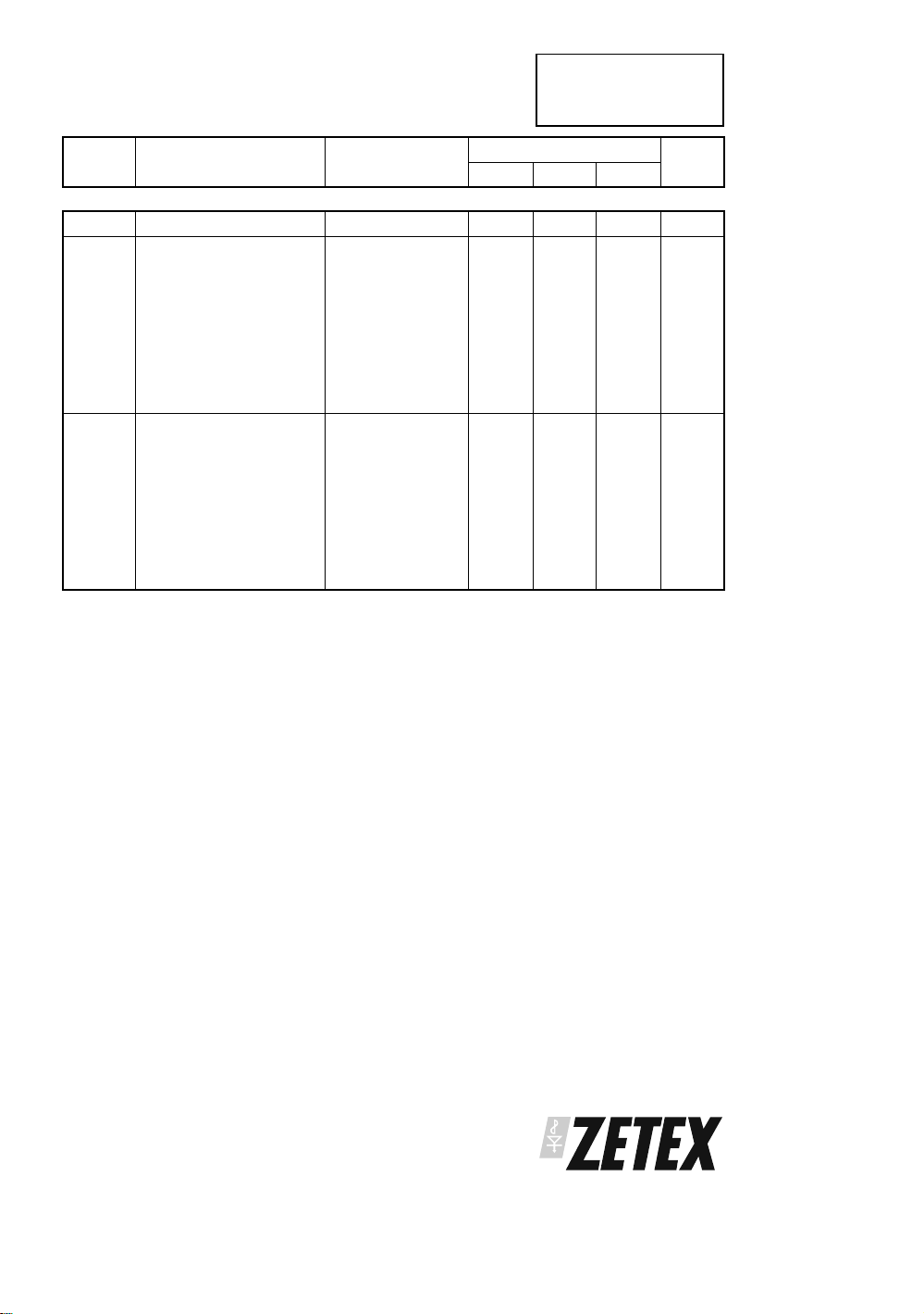
GATE CHARACTERISTICS
I
GO
V
OL
V
OH
V
OL
V
OH
Notes:
1. The negative bias voltages specified are generated on-chip using an internal oscillator. Two external capacitors, CNB and C
47nF are required for this purpose.
2. The characteristics are measured using two external reference resistors R
ground. For the ZNBR4000, resistor R
For the ZNBR6000, resistor R
3. Noise voltage is not measured in production.
4. Noise voltage measurement is made with FETs and gate and drain capacitors in place on all outputs. CG, 4.7nF, are conne cted between
gate outputs and ground, CD, 10nF, are connected between drain outputs and ground .
Output Current Range -30 2000
Output Voltage
ZNBR4000/1
Output Low ID1 to ID4=12mA
to IG4=0 -2.5 -1.8 V
I
G1
I
to ID4=12mA
D1
I
to IG4= -10µA
G1
-2.5 -1.8 V
Output High ID1 to ID4= 8mA
to IG4= 0 0 1 V
I
G1
Output Voltage
ZNBR6000/1
Output Low ID1 to ID6=12mA
to IG6= 0 -2.5 -1.8 V
I
G1
I
to ID6=12mA
D1
I
to IG6= -10µA
G1
-2.5 -1.8 V
Output High ID1 to ID6= 8mA
to IG6= 0 0 1 V
I
G1
and R
sets the drain current of FETs 1 and 2, resistor R
CAL1
sets the drain current of FETs 1 and 4, resistor R
CAL1
CAL1
of value 33kΩ wired from pins R
CAL2
sets the drain current of FETs 3 and 4.
CAL2
sets the drain current of FETs 2, 3, 5 and 6.
CAL2
µA
SUB
CAL1/2
, of
to
3
Page 4
ZNBR4000ZNBR4000 ZNBR4001
ZNBR6000 ZNBR6001
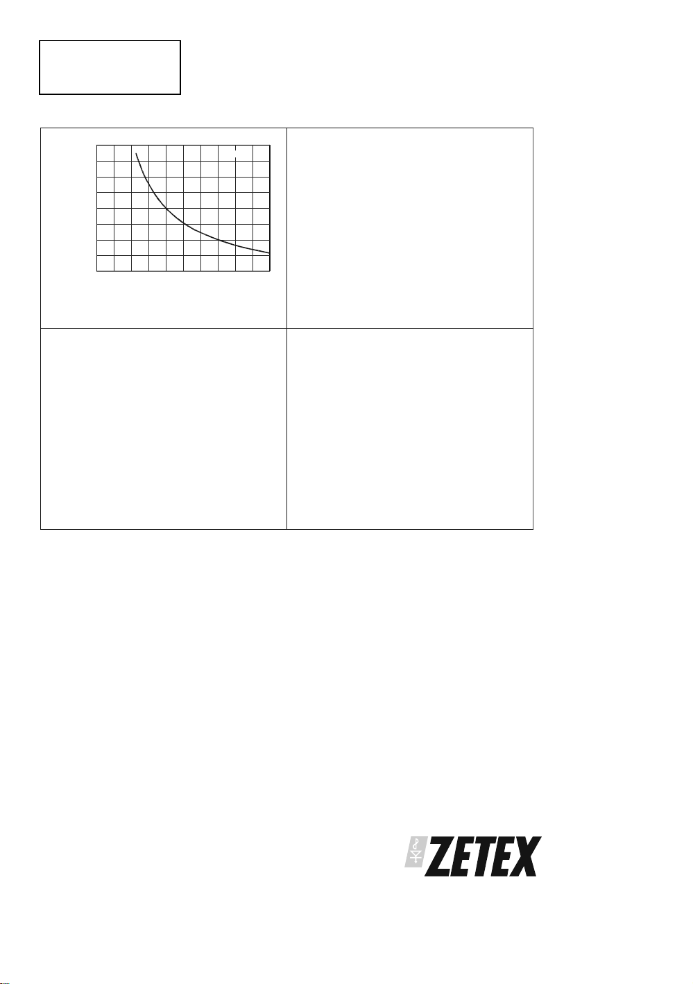
TYPICAL CHARACTERISTICS
16
14
12
10
8
6
4
Drain Current (mA)
2
0
0204060 100
R
cal
(k)
JFET Drain Current v R
Vcc = 5V
80
cal
4
Page 5
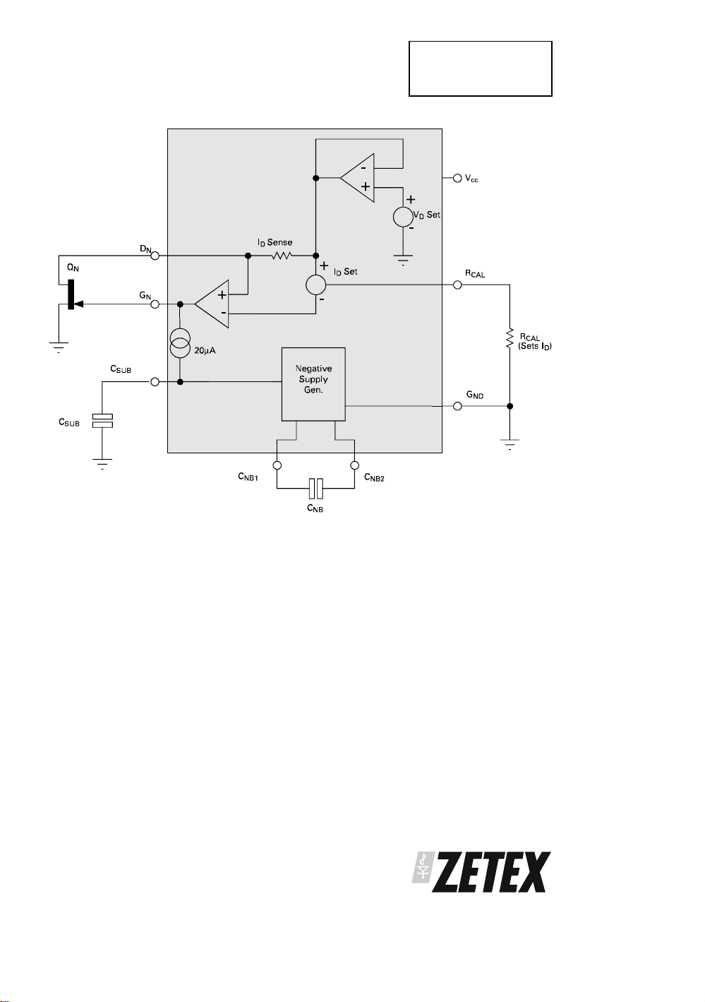
FUNCTIONAL DIAGRAM
ZNBR4000ZNBR4000 ZNBR4001
ZNBR6000 ZNBR6001
FUNCTIONAL DESCRIPTION
The ZNBR devices provide all the bias requirements for external FETs, including the generation
of the negative supply required for gate biasing, from the single supply voltage.
The diagram above shows a single stage from the ZNBR series. The ZNBR4000/1 contains 4 such
stages, the ZNBR6000/1 contains 6. The negative rail generator is common to all devices.
The drain voltage of the external FET Q
This is determined by the on board V
2.2 volts whilst the ZNBR4001/6001 provides nominally 2 volts.
The drain current taken by the FET is monitored by the low value resistor I
driving the gate of the FET adjusts the gate voltage of Q
the current called for by an external resistor R
different drain currents into selected FETs. Two R
resistor R
3 and 4. For the ZNBR6000, resistor R
sets the drain current of FETs 1 and 2, resistor R
CAL1
sets the drain current of FETs 2, 3, 5 and 6.
Since the FET is a depletion mode transistor, it is usually necessary to drive its gate negative with
respect to ground to obtain the required drain current. To provide this capability powered from
a single positive supply, the device includes a low current negative supply generator. This
generator uses an internal oscillator and two external capacitors, C
is set by the ZNBR device to its normal operating voltage.
N
Set reference, for the ZNBR4000/6000 this is nominally
D
Sense. The amplifier
so that the drain current taken matches
N
. Both ZNBR devices have the facility to program
CAL
sets the drain current of FETs 1 and 4, resistor R
CAL1
inputs are provided. For the ZNBR4000,
CAL
CAL2
D
sets the drain current of FETs
and C
NB
SUB
.
5
CAL2
Page 6
ZNBR4000ZNBR4000 ZNBR4001
ZNBR6000 ZNBR6001
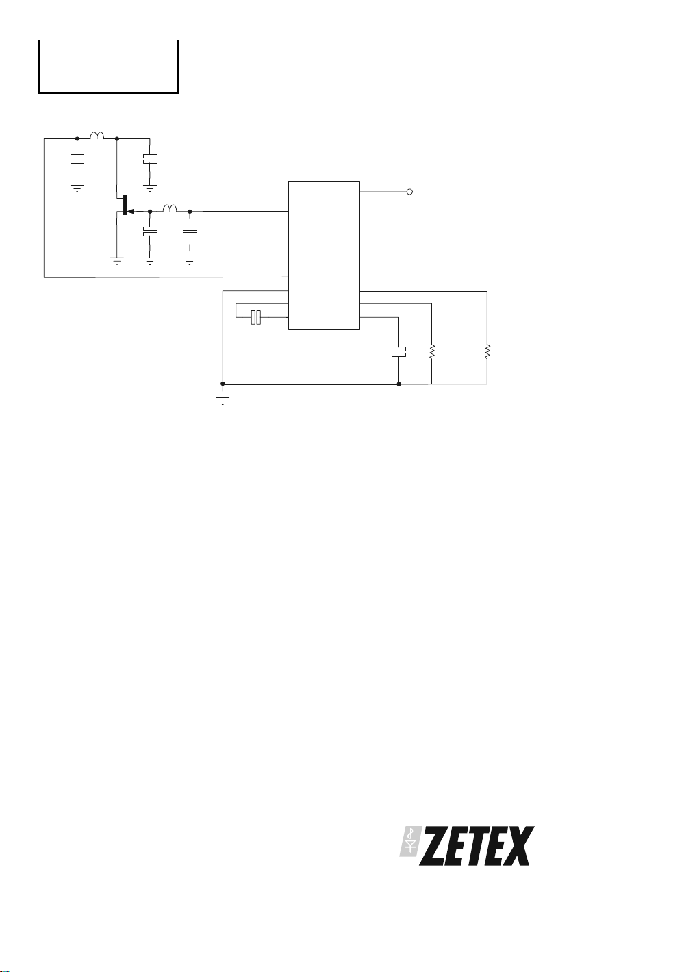
TYPICAL APPLICATION CIRCUIT
* L1
D
10nF
* C2C
Q1
* L2
* C3
* Stripline Elements
C
G
4.7nF
C
NB
47nF
ZNBR
G
N
D
N
G
ND
C
NB1
C
NB2
V
R
R
C
CC
CAL2
CAL1
SUB
C
SUB
47nF
R
CAL1
33k 33k
R
CAL2
APPLICATIONS INFORMATION
The above is a partial application circuit for the ZNBR series showing all external components
required for appropriate biasing. The bias circuits are unconditionally stable over the full
temperature range with the associated FETs and gate and drain capacitors in circuit.
Capacitors C
allowed to affect other external circuits which may be sensitive to RF interference. They also
serve to suppress any potential RF feedthrough between stages via the ZNBR device. These
capacitors are required for all stages used. Values of 10nF and 4.7nF respectively are
recommended however this is design dependent and any value between 1nF and 100nF could
be used.
The capacitors C
negative bias voltage is generated on-chip using an internal oscillator. The required value of
capacitors C
-3 volts. Although this generator is intended purely to bias the external FETs, it can be used to
power other external circuits via the C
Resistors R
have the facility to program different drain currents into selected FETs. Two R
provided. For the ZNBR4000, resistor R
sets the drain current of FETs 3 and 4. For the ZNBR6000, resistor R
FETs 1 and 4, resistor R
is required for all FETs on either device then pins R
shunted to ground by a single calibration resistor of half normal value.
If any bias control circuit is not required, its related drain and gate connections may be left open
circuit without affecting the operation of the remaining bias circuits. If all FETs associated with
a current setting resistor are omitted, the particular R
current can be reduced, if required, by using a high value R
and CG ensure that residual power supply and substrate generator noise is not
D
and C
NB
and C
NB
CAL1/2
SUB
sets the drain current at which all external FETs are operated. Both ZNBR devices
are an integral part of the ZNBRs negative supply generator. The
SUB
is 47nF. This generator produces a low current supply of approximately
pin.
SUB
inputs are
sets the drain current of FETs 1 and 2, resistor R
CAL1
sets the drain current of FETs 2, 3, 5 and 6. If the same drain current
CAL2
and R
CAL1
should still be included. The supply
CAL
CAL
sets the drain current of
CAL1
can be wired together and
CAL2
resistor (e.g. 470k).
CAL
CAL2
6
Page 7
ZNBR4000ZNBR4000 ZNBR4001
ZNBR6000 ZNBR6001
APPLICATIONS INFORMATION (Continued)
The ZNBR devices have been designed to protect the external FETs from adverse operating
conditions. With a JFET connected to any bias circuit, the gate output voltage of the bias circuit
can not exceed the range -3.5V to 0.7V, under any conditions including powerup and powerdown
transients. Should the negative bias generator be shorted or overloaded so that the drain current
of the external FETs can no longer be controlled, the drain supply to FETs is shut down to avoid
damage to the FETs by excessive drain current.
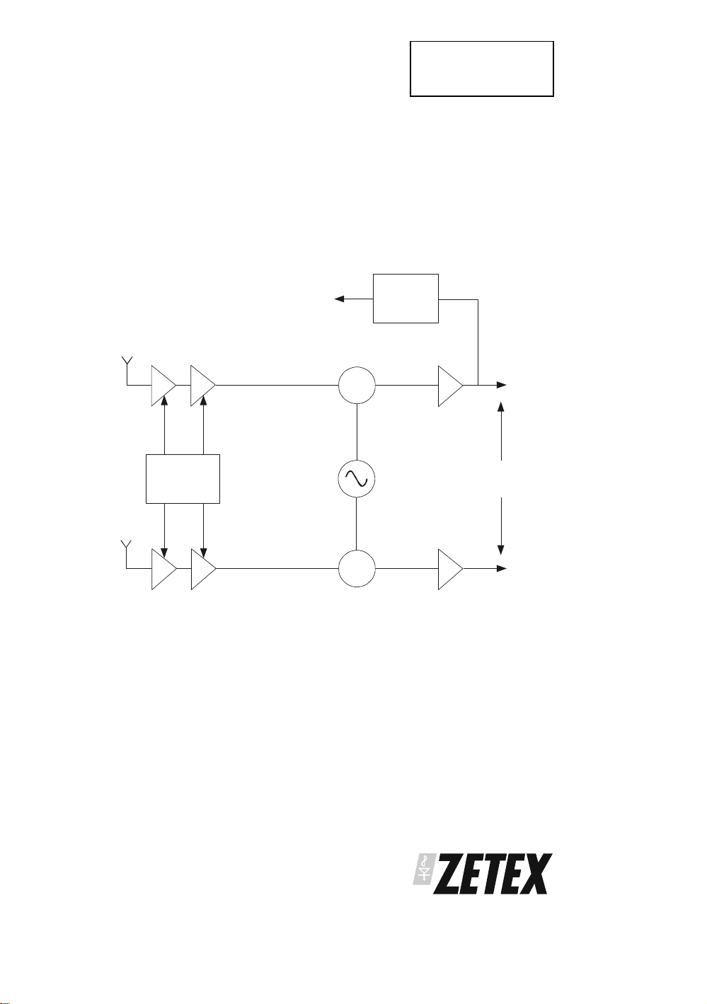
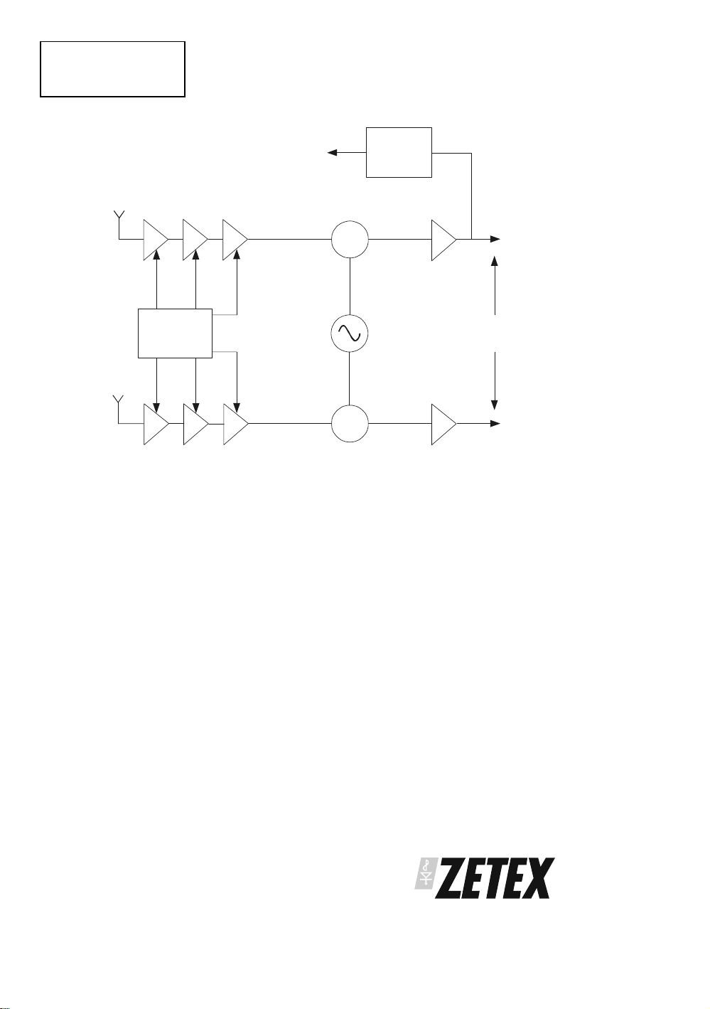
The following diagrams show the ZNBR4000/1 and ZNBR6000/1 in typical LNB applications.
Within each FET gain stage the numbering system indicates how the bias stages relate to the
application circuits. This is important when RCAL values are used to set differing drain currents.
Dual standard or enhanced LNB block diagram
Regula tor
ZHR Series
ASTRA
10.95 GHz-11.7 GHz
Standard Band
10.7 GHz-11.8 GHz
Enhanced Band
Ver tic al
Antenna
Horizontal
Antenna
Gain Stage
GaAs/HEMTFET
1
ZNBR4000/1
2
Gain Stage
GaAs/HEMTFET
Mixer
3
Local Osc
10.00 GHz - Standard Band
9.75 GHz - Enhanced Band
4
+
+
Mixer
Gain Stage
Vertical Channels
IF down feed
950-1750 MHz - Standard Band
950-2050 MHz - Enhanced Band
Horizontal Channels
Gain Stage
7
Page 8
ZNBR4000ZNBR4000 ZNBR4001
ZNBR6000 ZNBR6001
Dual standard or enhanced LNB block diagram. High Gain
Regula tor
ZHR Series
ASTRA
10.95 GHz-11.7 GHz
Standard Band
10.7 GHz-11.8 GHz
Enhanced Band
Ver tic al
Antenna
Horizontal
Antenna
Gain Stage
GaAs/HEMTFET
1
ZNBR6000/1
4
Gain Stage
GaAs/HEMTFET
32
Local Osc 2
10.00 GHz - Standard Band
9.75 GHz - Enhanced Band
56
Mixer
+
+
Mixer
Gain Stage
Vertical Channels
IF down feed
950-1750 MHz - Standard Band
950-2050 MHz - Enhanced Band
Horizontal Channels
Gain Stage
8
Page 9
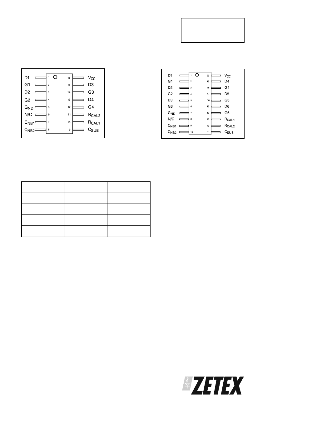
CONNECTION DIAGRAMS
ZNBR4000ZNBR4000 ZNBR4001
ZNBR6000 ZNBR6001
ZNBR4000
ZNBR4001
ORDERING INFORMATION
Part Number Package Part Mark
ZNBR4000Q16 QSOP16 ZNBR4000
ZNBR4001Q16 QSOP16 ZNBR4001
ZNBR6000Q20 QSOP20 ZNBR6000
ZNBR6001Q20 QSOP20 ZNBR6001
ZNBR6000
ZNBR6001
9
Page 10
ZNBR4000ZNBR4000 ZNBR4001
ZNBR6000 ZNBR6001
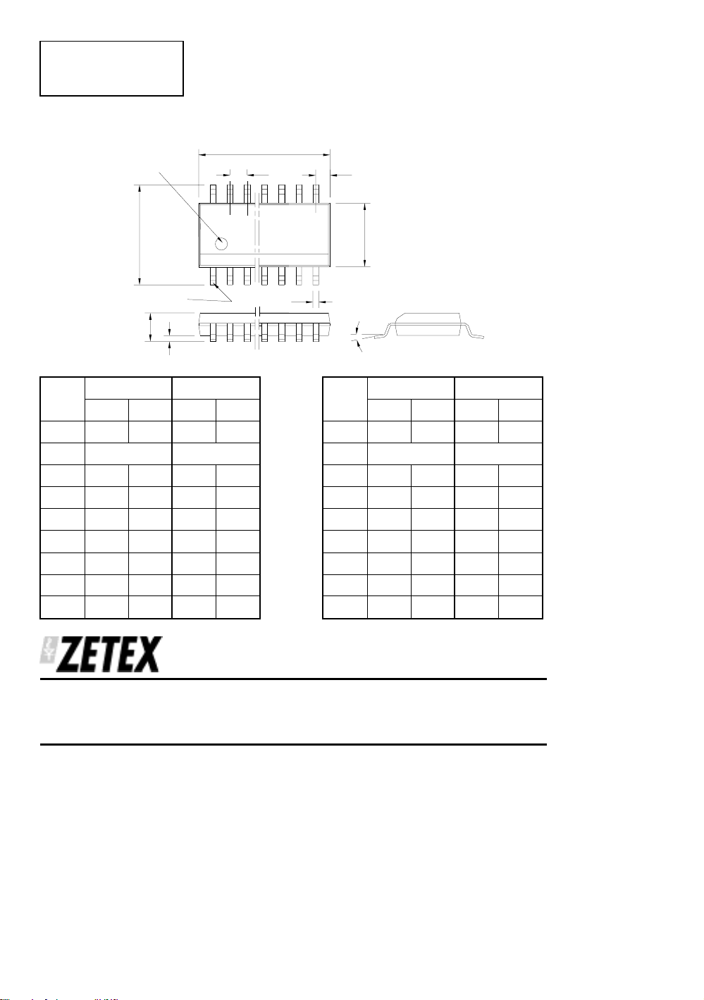
PACKAGE DIMENSIONS
IDENTIFICATION
RECESS
FOR PIN 1
A
B
C
J
PIN No.1
F
G
D
QSOP16
PIN Millimetres Inches
MIN MAX MIN MAX
A 4.80 4.90 0.033 0.039
B 0.635 0.025 NOM
C 0.177 0.267 0.007 0.011
D 0.20 0.30 0.008 0.012
E 3.81 3.99 0.15 0.157
F 1.35 1.75 0.053 0.069
G 0.10 0.25 0.004 0.01
J 5.79 6.20 0.228 0.244
K0° 8° 0° 8°
Zetex plc.
Fields New Road, Chadderton, Oldham, OL9-8NP, United Kingdom.
Telephone: (44)161 622 4422 (Sales), (44)161 622 4444 (General Enquiries)
Fax: (44)161 62 2 4420
Zetex GmbH Zetex Inc. Zetex (Asia ) Ltd. These are supp orted by
Streitfeldstraße 19 47 Mall Drive, Unit 4 3701-04 Metroplaza, Tower 1 agents and distributors in
D-81673 München Commack NY 11725 Hing Fong Road, major countries world-wide
Germany USA Kwai Fong, Hong Kong Zetex plc 2001
Telefon: ( 49) 89 45 49 49 0 Telephone: (631) 543-7 100 Teleph one:(852) 26 100 611
Fax: (49) 89 45 49 49 49 Fax: (631) 864-7630 Fax: (852) 24250 494 http://www.zetex. com
This publication is issued to provide outline information only which (unless agreed by the Company in writing) may not be used, applied
or reproduced for any purpose or form part of any order or contract or be regarded as a representation relating to the products or
services concerned. The Company reserves the right to alter without notice the specification, design, price or conditions of supply of
any product or service.
E
K
QSOP20
PIN Millimetres Inches
MIN MAX MIN MAX
A 8.55 8.74 0.337 0.344
B 0.635 0.025 NOM
C 1.42 1.52 0.056 0.06
D 0.20 0.30 0.008 0.012
E 3.81 3.99 0.15 0.157
F 1.35 1.75 0.053 0.069
G 0.10 0.25 0.004 0.01
J 5.79 6.20 0.228 0.244
K0° 8° 0° 8°
12
 Loading...