

Page 1
Synchronous Step-Down MOSFET Drivers
ZL1505
ZL1505
The ZL1505 is an integrated high-speed, high-current
N-channel MOSFET driver for synchronous step-down
DC-DC conversion applications. When used with Zilker
Labs Digital-DC™ PWM controllers, the ZL1505 enables
dynamically adaptive dead-time control that optimizes
efficiency under all operating conditions. A dual input
PWM configuration enables this efficiency optimization
while minimizing complexity within the driver.
Operating from a 4.5V to 7.5V input, the ZL1505
combines a 5A, 0.5W low-side driver and a 3A, 0.8W
high-side driver to support high step-down buck
applications. A unique adjustable gate drive current
scheme allows the user to adjust the drive current on
both drivers to optimize performance for a wide rage of
input/output voltages, load currents, power MOSFET s
and switching frequencies up to 1.4MHz. An integrated
30V bootstrap Schottky diode is used to charge the
external bootstrap capacitor. An internal w atchdog circuit
prevents excessive shoot-through currents and protects
the external MOSFET switches.
The ZL1505 is specified over a wide -40°C to +125°C
junction temperature range and is available in an
exposed pad DFN-10 package.
Features
• High-speed, high-current drivers for synchronous
N-channel MOSFETs
• Adaptive dead-time control optimizes efficiency
when used with Digital-DC controllers
• Integrated 30V bootstrap Schottky diode
• Capable of driving 40A per phase
• Supports switching frequency up to 1.4MHz
- >4A source, >5A sink low-side driver
- >3A source/sink high-side driver
- <10ns rise/fall times, low propagation delay
• Adjustable gate drive strength optimizes efficiency
, V
, I
for different V
combinations
• Internal non-overlap watchdog prevents
shoot-through currents
IN
OUT
, FSW and MOSFET
OUT
Applications*(see page 12)
• High efficiency, high-current DC/DC buck converters
with digital control and PMBus™
• Multi-phase digital DC/DC converters with phase
adding/dropping
•Power train modules
• Synchronous rectification for secondary side isolated
power converters
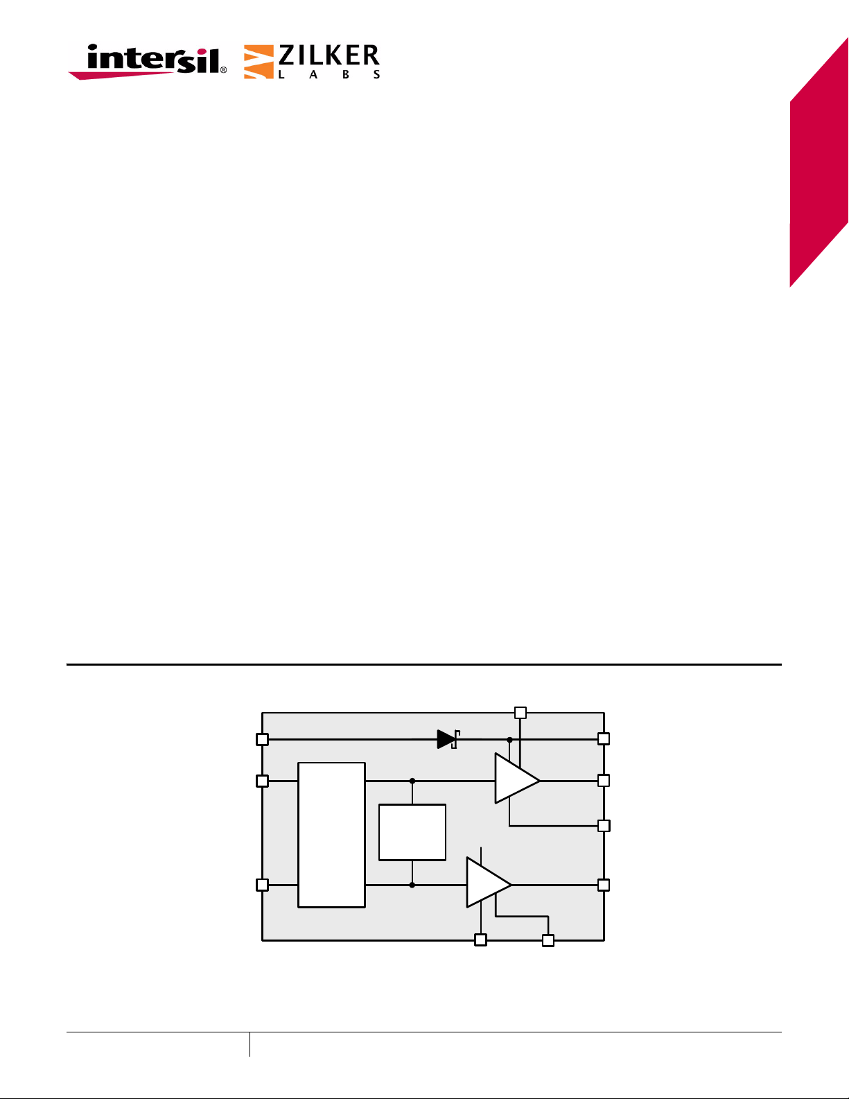
VDD
PWMH
PWML
Related Literature*(see page 12)
• FN6846 ZL2004 Data Sheet
HSEL
Level
shift
Shoot-
through
Protection
VDD
ZL1505
GND
FIGURE 1. ZL1505 BLOCK DIAGRAM
BST
GH
SW
GL
LSEL
December 4, 2009
FN6845.1
1
CAUTION: These devices are sensitive to electrostatic discharge; follow proper IC Handling Procedures.
1-888-INTERSIL or 1-888-468-3774
| Intersil (and design) is a registered trademark of Intersil Amer ic as Inc .
All other trademarks mentioned are the property of their respective owners.
Copyright Intersil Americas Inc. 2009. All Rights Reserved
Page 2
ZL1505
Typical Application Circuit
The following application circuit represents the typical implementation of the ZL1505 (Notes 1, 2).
V
IN
4.5-14V
V
BIAS
4.5-7.5V
VMON
VIN
PWMH
PWMH
PWMH
ZL2004
PWML
XTEMP
VSEN+
SGND
VSEN-
PWML
TEMP+
ISENA
ISENB
FIGURE 2. POWER TRAIN MODULE USING ZL2004 PWM CONTROLLER
NOTES:
1. For V
specified in Figure 2.
2. V
of 4.5V to 7.5V, the maximum VIN of the ZL1505 is 22.5V to 25.5V. ZL1505 input supply voltage range (VIN) is
DD
for this application circuit is limited by the ZL2004 VIN of 4.5V to 14V.
IN
PWML
TEMP-
VDD
HSEL
LSEL
ZL1505
VINVDD
Power Train
Module
GH
BST
SW
GL
GND
GND
CS-CS+
VOUT
GND
2
FN6845.1
December 4, 2009
Page 3
Pin Configuration
ZL1505
ZL1505
(10 LD DFN)
TOP VIEW
HSEL
GH
SW
PWMH
PWML
1
2
*EPAD
3
4
5
*CONNECT TO GND
BST
10
VDD
9
GL
8
7
GND
LSEL
6
Pin Descriptions
PIN NUMBER PIN NAME TYPE (Note 3) DESCRIPTION
1 HSEL I High-side gate drive current selector. Connect to BST for maximum gate
drive current; Connect to SW for 50% of maximum gate drive current.
2 GH O Output of high-side gate driver. Connect to the gate of high-side FET.
3 SW I/O Phase node. Return path for high-side driver. Connect to source of high-side
4 PWMH I High-side PWM control input.
5 PWML I Low-side PWM control input.
6 LSEL I Low-side gate drive current selector. Connect to VDD for maximum gate
FET and drain of low-side FET.
drive current; Connect to GND for 50% of maximum gate drive current.
7 GND PWR Ground. All signals return to this pin.
8 GL O Output of low-side gate driver. Connect to the gate of low-side FET.
9 VDD PWR Gate drive bias supply . Connect a high quality bypass capacitor from this pin
to GND.
10 BST PWR Bootstrap supply. Connect external capacitor to SW node.
ePad GND PWR Ground.
NOTE:
3. I = Input, O = Output, PWR = Power OR Ground.
Ordering Information
PACKAGE
PART NUMBER
(Notes 4, 5, 6)
PART
MARKING
TEMP RANGE
(°C)
Tape and Reel
(Pb-free)
ZL1505ALNNT 1505 -40 to +125 10 Ld 3x3 DFN L10.3x3D
ZL1505ALNNT1 1505 -40 to +125 10 Ld 3x3 DFN L10.3x3D
NOTES:
4. Please refer to TB347
for details on reel specifications.
5. These Intersil Pb-free plastic packaged products employ special Pb-free material sets; molding compounds/die attach
materials and NiPdAu plate - e4 termination finish, which is RoHS compliant and compatible with both SnPb and Pb-free
soldering operations. Intersil Pb-free products are MSL classified at Pb-free peak reflow temperatures that meet or exceed
the Pb-free requirements of IPC/JEDEC J STD-020.
6. For Moisture Sensitivity Level (MSL), please see device information page for ZL1505
techbrief TB363
.
. For more information on MSL please see
PKG.
DWG. #
3
FN6845.1
December 4, 2009
Page 4
ZL1505
Absolute Maximum Ratings Thermal Information
Voltage Measured with Respect to GND
DC Supply Voltage for VDD Pin . . . . . . . . . . . . .-0.3V to 8V
High-Side Supply Voltage for BST Pin . . . . . . . . -0.3V to 30V
High-Side Drive Voltage for
GH Pin . . . . . . . . . . . . . . . (V
Low-Side Drive Voltage for
GL Pin . . . . . . . . . . . . . . . .(GND - 0.3V) to (V
Boost to Switch Differential (V
BST, SW Pins . . . . . . . . . . . . . . . . . . . . . . . .-0.3V to 8V
SW
- VSW) for
BST
- 0.3V) to (V
BST
DD
+ 0.3V)
+ 0.3V)
Switch Voltage for SW Pin
Continuous . . . . . . . . . . . . . . . . . . . (GND - 0.3V) to 30V
<100ns . . . . . . . . . . . . . . . . . . . . . . .(GND - 5V) to 30V
Logic I/O Voltage for PWMH, PWML, LSEL Pins. . .-0.3V to 8V
HSEL Pin . . . . . . . . . . . . . (V
ESD Rating
- 0.3V) to (V
SW
BST
+ 0.3V)
Human Body Model . . . . . . . . . . . . . . . . . . . . . . . . . 2kV
GL Pin . . . . . . . . . . . . . . . . . . . . . . . . . . . . . . . . 1.5kV
Machine Model . . . . . . . . . . . . . . . . . . . . . . . . . . . 500V
Latch Up . . . . . . . . . . . . . . . . . . . . . . . . Tested to JESD78
CAUTION: Do not operate at or near the maximum ratings listed for extended periods of time. Exposure to such conditions may adversely impact
product reliability and result in failures not covered by warranty.
NOTES:
7. θJA is measured in free air with the component mounted on a high effective thermal conductivit y test board with “direct attach”
features. See Tech Brief TB379.
8. For θ
, the “case temp” location is the center of the exposed metal pad on the package underside.
JC
Thermal Resistance (Typical) θ
(°C/W) θJC (°C/W)
JA
10 Ld DFN (Notes 7, 8). . . . . . . . . 50 7
Junction Temperature Range . . . . . . . . . . -55°C to +150°C
Storage Temperature Range . . . . . . . . . . . -55°C to +150°C
Pb-Free Reflow Profile . . . . . . . . . . . . . . . . . .see link below
http://www.intersil.com/pbfree/Pb-FreeReflow.asp
Recommended Operating Conditions
Gate Drive Bias Supply Voltage Range
VDD . . . . . . . . . . . . . . . . . . . . . . . . . . . . . .4.5V to 7.5V
Input Supply Voltage Range, V
Operating Junction Temperature Range, TJ. . -40°C to +125°C
. . . . . . . . 3V to 30V - V
IN
DD
Electrical Specifications V
PARAMETER CONDITIONS
= 6.5V, TJ = -40°C to +125°C unless otherwise noted. Typica l values are at
DD
T
=+25°C. Boldface limits apply over the operating temperature range,
A
-40°C to +125°C.
MIN
(Note 9) TYP
MAX
(Note 9) UNIT
BIAS CURRENT CHARACTERISTICS
I
supply current Not switching – 110 180 µA
DD
PWM INPUT CHARACTERISTICS
PWM input bias current V
PWM input logic low, V
PWM input logic high, V
IL
IH
= 5 V –5–µA
PWM
V
= 0 V ––1µA
PWM
PWMH or PWML VDD = 6.5V 1.7 2 2.2 V
V
= 5.0 V 1.5 1.7 1.9 V
DD
PWMH or PWML VDD = 6.5V 2.8 3.1 3.4 V
VDD = 5.0V 2.2 2.5 2.7 V
Hysteresis PWMH or PWML V
Minimum PWMH On-time to Produce GH
Pulse, t
PWMH,ON
Minimum GH On-time pulse, t
(Note 11)
(Note 10)
GH,ON
= 0 – 8.5 12 ns
C
GH
CGH = 0 – 10 14 ns
C
GH
= 3 nF, V
HSEL
= V
BST
= 6.5V - 1.1 - V
DD
V
= 5.0V - 0.8 - V
DD
-1420 ns
Minimum PWMH Off-time to Produce
Valid GH Pulse, t
PWMH,OFF
BOOTSTRAP DIODE CHARACTERISTICS
Forward Voltage (V
) Forward bias current 100 mA – 0.8 – V
F
4
CGH = 0 – 13 17 ns
FN6845.1
December 4, 2009
Page 5

ZL1505
Electrical Specifications V
PARAMETER CONDITIONS
= 6.5V, TJ = -40°C to +125°C unless otherwise noted. Typica l values are at
DD
T
=+25°C. Boldface limits apply over the operating temperature range,
A
-40°C to +125°C. (Continued)
MIN
(Note 9) TYP
MAX
(Note 9) UNIT
THERMAL PROTECTION
Thermal trip point –150– °C
Thermal reset point –134– °C
UPPER GATE DRIVER CHARACTERISTICS
Driver Voltage (V
High-side Driver Peak Gate Drive
Current (Pull-up)
– VSW) –6– V
BST
(VGH – VSW) = 2.5V HSEL connected
2.0 3.2 – A
to BST
HSEL connected
1.0 1.7 - A
to SW
High-side Driver Peak Gate Drive
Current (Pull-down)
– VSW) = 2.5V HSEL connected
(V
GH
to BST
HSEL connected
2.0 3.2 – A
1.0 1.6 - A
to SW
High-side Driver Pull-up Resistance (V
– VGH) = 50mV HSEL connected
BST
to BST
HSEL connected
–0.70.9 Ω
-0.91.2 Ω
to SW
High-side Driver Pull-down Resistance (V
– VSW) = 50mV HSEL connected
GH
to BST
HSEL connected
–0.81.1 Ω
1.1 1.5 Ω
to SW
LOWER GATE DRIVER CHARACTERISTICS
Driver voltage (V
Low-side Driver Peak Gate Drive Current
(Pull-up)
) -6.5- V
DD
(V
GL
- V
) = 2.5V LSEL connected
GNG
to VDD
LSEL connected
3.0 4.5 – A
1.5 2.4 - A
to GND
Low-side Driver Peak Gate Drive Current
(Pull-down)
(V
GL
– V
) = 2.5V LSEL connected
GND
to VDD
LSEL connected
3.5 5.4 – A
1.8 2.8 - A
to GND
Low-side Driver Pull-up Resistance (V
- VGL) = 50mV LSEL connected
DD
–0.70.9 Ω
to VDD
LSEL connected
-1.01.3 Ω
to GND
Low-side Driver Pull-down Resistance (V
– GND) = 50mV LSEL connected
GL
to VDD
LSEL connected
–0.50.7 Ω
-0.71.0 Ω
to GND
SWITCHING CHARACTERISTICS
GH rise time, t
RH
CGH = 3nF HSEL connected
–5.38.5 ns
to BST
HSEL connected
-10.516.5 ns
to SW
5
FN6845.1
December 4, 2009
Page 6

ZL1505
Electrical Specifications V
PARAMETER CONDITIONS
GH fall time, t
GL rise time, t
GL fall time, t
GH turn-on propagation delay, t
GH turn-off propagation delay, t
GL turn-on propagation delay, t
GL turn-off propagation delay, t
NOTES:
9. Parameters with MIN and/or MAX limits are 100% tested at +25°C, unless otherwise specified. T emper ature limits established
by characterization and are not production tested.
10. The minimum PWMH on-time pulse (t
edge.
11. The minimum GH on-time pulse (t
FH
RL
FL
DLR
DLF
= 6.5V, TJ = -40°C to +125°C unless otherwise noted. Typica l values are at
DD
T
=+25°C. Boldface limits apply over the operating temperature range,
A
-40°C to +125°C. (Continued)
MIN
(Note 9) TYP
DHR
DHF
CGH = 3nF HSEL connected
to BST
HSEL connected
to SW
CGL = 3nF LSEL connected
CGL = 3nF LSEL connected
HSEL connected to BST –30.0– ns
HSEL connected to SW - 31.5 - ns
HSEL connected to BST –37.5– ns
HSEL connected to SW - 39.0 - ns
LSEL connected to V
LSEL connected to GND - 28.0 - ns
LSEL connected to V
LSEL connected to GND - 31.5 - ns
PWMH,ON
GH,ON
) is specified from VPWM = 2.5V on the rise edge to VPWM = 2.5V on the falling
) is specified at VGH = 2.5V.
DD
DD
to VDD
LSEL connected
to GND
to VDD
LSEL connected
to GND
-4.87.5 ns
-9.515 ns
–4.06.0 ns
-7.812 ns
-3.04.5 ns
-5.58.5 ns
–26.5– ns
–30.0– ns
MAX
(Note 9) UNIT
PWM
GH
2.5V 2.5V
t
PWMH,ON
t
DLF
t
DLR
90% 90%
2.5V 2.5V
t
10%
t
RH
FIGURE 3. TIMING DIAGRAM
GH,ON
6
10%
t
FH
FN6845.1
December 4, 2009
Page 7

Typical Performance Curves
)
)
130
ZL1505
155
120
110
100
IVDD (uA)
90
80
70
4.5 5 5.5 6 6.5 7 7.5
VDD (V)
-25 °C
25 °C
85 °C
FIGURE 4. IVDD vs VDD WITH TEMPERATURE (NO
SWITCHING)
22
20
18
16
14
On-time (ns
12
10
8
4.5 5 5.5 6 6.5 7 7.5
CGH=0
CGH=3nF, HSEL=BST
CGH=3nF, HSEL=SW
VDD (V)
150
145
140
T (C)
135
130
125
120
4.555.566.577.5
VDD (V)
Trising
Tfalling
FIGURE 5. THERMAL PROTECTION THRESHOLDS
16
15
14
13
12
11
On-t ime (ns
10
9
8
4.5 5 5.5 6 6.5 7 7.5
VDD (V)
-25 °C
25 °C
85 °C
FIGURE 6. MINIMUM GH ON-TIME, t
T
= +25°C)
A
GH,ON
(Note 12,
FIGURE 7. t
GH,ON
C
GH
WITH TEMPERATURE (Note 13,
= 0)
NOTES:
12. Performance curves with temperature are measured at ambient temperatures (T
13. t
timing is shown in Figure 3.
GH,ON
7
) of +85°C, +25°C and -25°C.
A
FN6845.1
December 4, 2009
Page 8

)
ZL1505
Typical Performance Curves (Continued)
16
14
12
10
30
26
22
-25 °C
25 °C
85 °C
8
On-ti me (ns
6
4
2
4.555.566.577.5
VDD (V)
-25 °C
25 °C
85 °C
FIGURE 8. MINIMUM PWMH ON-TIME, t
(CGH= 0)
6.6
5.6
4.6
3.6
IGL (A)
2.6
1.6
0.6
4.5 5 5.5 6 6.5 7 7.5
VDD (V)
LSEL=VDD
LSEL=GND
PWMH,ON
18
Off-time (ns)
14
10
4.5 5 5.5 6 6.5 7 7.5
VDD (V)
FIGURE 9. MINIMUM PWMH OFF-TIME, t
(CGH= 0)
6.6
5.6
4.6
IGL (A)
3.6
2.6
1.6
4.5 5 5.5 6 6.5 7 7.5
VDD (V)
-25 °C
25 °C
85 °C
PWMH,OFF
FIGURE 10. LOW-SIDE DRIVER PULL-UP CURRENT
(V
= 2.5V, TA = +25°C)
GL
8
7
6
5
IGL (A)
4
3
2
1
4.5 5 5.5 6 6.5 7 7.5
VDD (V)
LSEL=VDD
LSEL=GND
FIGURE 12. LOW-SIDE DRIVER PULL-DOWN
CURRENT (V
= 2.5V, TA = +25°C)
GL
8
FIGURE 11. LS PULL-UP CURRENT WITH
TEMPERATURE (V
8
7
6
IGL (A)
5
4
3
4.555.566.577.5
VDD (V)
= 2.5V, LSEL = VDD)
GL
-25 °C
25 °C
85 °C
FIGURE 13. LS PULL-DOWN CURRENT WITH
TEMPERATURE (VGL = 2.5V, LSEL = VDD)
December 4, 2009
FN6845.1
Page 9

ZL1505
Typical Performance Curves (Continued)
12
11
10
9
8
7
trise (ns)
6
5
4
3
4.5 5 5.5 6 6.5 7 7.5
VDD (V)
LSEL=VDD
LSEL=GND
6.5
6
5.5
5
4.5
trise (ns)
4
3.5
3
4.555.566.577.5
VDD (V)
-25 °C
25 °C
85 °C
FIGURE 14. LOW-SIDE DRIVER RISE TIME, t
(CGL= 3nF, TA = +25°C)
7
6
5
tfall (ns)
4
3
2
4.555.566.577.5
VDD (V)
LSEL=VDD
LSEL=GND
FIGURE 16. LOW-SIDE DRIVER FALL TIME, t
(CGL=3nF, TA = +25°C)
5
4
RL
FL
FIGURE 15. t
4.5
4
3.5
tfall (ns)
3
2.5
2
4.5 5 5 .5 6 6 .5 7 7.5
FIGURE 17. t
5
4.5
4
WITH TEMPERATURE (CGL = 3nF,
RL
LSEL = VDD)
VDD (V)
WITH TEMPERATURE (CGL = 3nF,
FL
LSEL = VDD)
-25 °C
25 °C
85 °C
3
IGH (A)
2
1
0
4.555.566.577.5
VDD (V)
HSEL=BST
HSEL=SW
FIGURE 18. HIGH-SIDE DRIVER PULL-UP CURRENT
(V
- VSW = 2.5V, TA = +25°C)
GH
9
3.5
3
IGH (A)
2.5
2
1.5
1
4.5 5 5.5 6 6.5 7 7.5
VDD (V)
-25 °C
25 °C
85 °C
FIGURE 19. HS PULL-UP CURRENT WITH
TEMPERATURE (V
HSEL = BST)
- VSW = 2.5V,
GH
FN6845.1
December 4, 2009
Page 10

ZL1505
Typical Performance Curves (Continued)
5
4
3
IGH (A)
2
1
HSEL=BST
0
HSEL=SW
4.5 5 5.5 6 6.5 7 7.5
VDD (V)
FIGURE 20. HIGH-SIDE DRIVER PULL-DOWN
17.5
15.5
13.5
11.5
CURRENT (V
T
=+25°C)
A
- VSW = 2.5V,
GH
HSEL=BST
HSEL=SW
5
4.5
4
3.5
IGH (A)
3
2.5
2
1.5
4.5 5 5.5 6 6.5 7 7.5
VDD (V)
-25 °C
25 °C
85 °C
FIGURE 21. HS PULL-DOWN CURRENT WITH
TEMPERATURE (V
HSEL = BST)
8.5
7.5
6.5
- VSW = 2.5V,
GH
-25 °C
25 °C
85 °C
9.5
trise (ns)
7.5
5.5
3.5
4.5 5 5.5 6 6.5 7 7.5
VDD (V)
FIGURE 22. HIGH-SIDE DRIVER RISE TIME, t
(CGH= 3nF, TA = +25°C)
11.5
9.5
7.5
tfall (ns)
5.5
3.5
4.5 5 5.5 6 6.5 7 7.5
VDD (V)
HSEL=BST
HSEL=SW
RH
trise (ns)
5.5
4.5
3.5
4.555.566.577.5
VDD (V)
FIGURE 23. t
7.5
6.5
5.5
tfall (ns)
4.5
3.5
4.5 5 5.5 6 6.5 7 7.5
WITH TEMPERATURE (CGH = 3nF,
RH
HSEL = BST)
VDD (V)
-25 °C
25 °C
85 °C
FIGURE 24. HIGH-SIDE DRIVER FALL TIME, t
(CGH= 3nF, TA = +25°C)
10
FH
FIGURE 25. t
WITH TEMPERATURE (CGH = 3nF,
FH
HSEL = BST)
December 4, 2009
FN6845.1
Page 11

ZL1505
ZL1505 Overview
Theory of Operation
The ZL1505 is a synchronous N-channel MOSFET driver
that is intended for use with Zilker Labs Digital-DC PWM
controllers to enable a high-efficiency DC/DC conversion
scheme. The patented Digital-DC control scheme utilizes
a closed-loop algorithm to optimize the dead-time
applied between the gate drive signals for the high-side
and low-side MOSFETs. By monitoring the duty cycle of
the resulting DC/DC converter circuit, this dynamic
routine continuously varies the MOSFET dead times to
optimize conversion efficiency in response to varying
circuit conditions. The ZL1505’s dual PWM input
configuration enables this optimization scheme to be
applied while minimizing the complexity within the driver
device. Please refer to the ZL2004 data sheet for details
on the dynamic dead-time optimization routine.
The ZL1505 integrates two powerful gate drivers that
have been optimized for step-down DC/DC con version
circuit configurations whose output current can exceed
40A per phase. The ZL1505 also integrates a 30V
bootstrap Schottky diode to minimize the external
components and provide a high drive voltage to the
high-side driver device.
condition ceases, allowing normal switching operation to
continue.
Start-up Requirements
During power-up, the ZL1505 maintains both GH and GL
outputs in the LOW state while the V
ramping up. Once the VDD supply is within specification,
the GH and GL pins may be oper ated using th e PWMH
and PWML logic inputs respectively.
In the case where the PWM controller is powered from a
supply other than the ZL1505’s V
controller is powered up first, the PWM controller gate
outputs should be kept in low or in high-impedance state
until the V
the ZL1505 begins its power-down sequence prior to the
PWM controller then the PWM controller gate outputs
should be set in low or in high-impedance state before
the V
DD
supply is within specification. Additionally , if
DD
voltage supply drops below its specified range.
voltage is
IN
supply , and the PWM
DD
Thermal protection
When the junction temperature exceeds +150°C the
high-side driver output GH is forced to logic low state.
The driver output is allowed to switch logic states again
once the junction temperature drops below +134°C.
Variable Gate Drive Current
The ZL1505 incorporates an innovative variable drive
current scheme that enables the user to optimize the
gate drive current levels to the requirements of the
external MOSFET s used ov er a wide r ange of oper ating
frequencies. Each of the gate drivers incorporates a logic
input (HSEL and LSEL) that allows the user to select the
gate drive strength to 50% or 100% of the total rated
drive current.
With the HSEL pin connected to the BST pin, the
high-side driver can deliver the full rated gate drive
current; with the HSEL pin connected to the SW pin, the
output current will be limited to 50% of the full rated
output capability. With the LSEL pin connected to VDD,
the low-side driver can deliver the full rated gate drive
current; with the LSEL pin connected to GND, the output
current will be limited to 50% of the full rated output
capability . Using HSEL and LSEL, the ZL1505 can be used
across a wide range of applications using only a simple
PCB layout change.
Also, the VDD pin is the gate drive bias supply for the
external MOSFET s. VDD can be used to vary the gate
drive strength as shown for the low-side driver in
Figures 9 thru 12 and for the high-side driver in
Figures 17 thru 20.
Overlap Protection Circuit
The ZL1505 includes an internal watchdog circuit that
prevents excessive shoot-through current from occurring
in the unlikely event that the PWM converter places both
switches in the ON position. If the overlap time between
the PWMH and PWML pulses exceeds 30ns, the PWMH
signal will be forced to the LOW state until the overlap
11
FN6845.1
December 4, 2009
Page 12

ZL1505
Revision History
The revision history provided is for informational purposes only and is believed to be accurate, but not warranted. Please go to
web to make sure you have the latest Rev.
DATE REVISION CHANGE
12/4/09 FN6845 .1 Converted to new Intersil template. Changed in Abs Max Ratings “Low- Side Driv e Voltage for
GL pin” from “(GND - 0.3) to (VIN + 0.3)” to “(GND - 0.3) to (VDD + 0.3)”. Removed Bullet
"Adjustable gate drive voltage: 4.5V to 7.5V" and "Exposed pad 3mmx3mm DFN -10 Package"
from Features. Intersil Standards applied are: Added Related Information, Updated ordering
information with Notes that includes MSL. Updated Abs Max Ratings with notes, added ESD
Ratings and Latchup, added Boldface text in Electrical Spec Table. Added POD
2/14/09 FN6845.0 Assigned file number FN6845 to datasheet as this will be the first release with an Intersil fil e
number. Replaced header and footer with Intersil header and footer. Updated disclaimer
information to read “Intersil and it’s subsidiaries including Zilker Labs, Inc.” No changes to
datasheet content
Products
Intersil Corporation is a leader in the design and manufacture of high-performance analog semiconductors. The
Company's products address some of the industry's fastest growing markets, such as, flat panel displays, cell phones,
handheld products, and notebooks. Intersil's product families address power management and analog signal
processing functions. Go to www.intersil.com/products
*For a complete listing of Applications, Related Documentation and Related Parts, please see the respective device
information page on intersil.com: ZL1505
To report errors or suggestions for this datasheet, please go to www.intersil.com/askourstaff
FIT s are available from our website at http://rel.intersil.com/reports/search.php
for a complete list of Intersil product families.
For additional products, see www.intersil.com/product_tree
Intersil products are manufactured, assembled and tested utilizing ISO9000 quality systems as noted
in the quality certifications found at www.intersil.com/design/quality
Intersil products are sold by description o nly . In tersil Corporation reserves the right to make change s in c irc uit design, software and/or specifications
at any time without notice. Accordingly, the reader is cautioned to verify that data sheets are current before placing orders. Information furnished by
Intersil is believed to be accurate and reliable. However, no responsibility is assumed by Intersil or its subsidiaries for its use; nor for any
infringements of patents or other rights of third parties which may result from its use. No license is granted by implication or otherwise under any
patent or patent rights of Intersil or its s ub si di arie s .
For information regarding Intersil Corporation and its products, see www.intersil.com
12
FN6845.1
December 4, 2009
Page 13

Dual Flat No-Lead Plastic Package (DFN)
ZL1505
8.
0.20 DIA TYP
0.10 C
2X
2X
9.
PIN #1 ID
E2
K
SEE DETAIL "A"
0.10 C
0.10 C
0.05 C
SEATING PLANE
(DATUM A)
R0.20
E2/2
5.
L
e
D
N N-1
2
1
TOP VIEW
A
A1
SIDE VIEW
D2
D2/2
2
1
N N-1
e
(ND-1) X e
BOTTOM VIEW
DATUM A OR B
11. 11.
L1
e/2
TERMINAL TIP
A
B
L10.3x3D
10 LEAD DUAL FLAT NO-LEAD PLASTIC PACKAGE
MILLIMETERS
SYMBOL
E
A 0.80 0.85 0.90 -
A1 0.00 0.02 0.05 -
NOTESMIN NOMINAL MAX
A3 0.20 REF -
θ 0-122
K 0.20 MIN
D 3.00 BSC -
D2 2.20 2.30 2.40 -
E 3.00 BSC -
E2 1.50 1.60 1.70 -
C
L 0.35 0.40 0.45 12
L1 0.15mm MAX 11
b 0.18 0.25 0.30 4
e 0.50 BSC N103
ND 5 5
Rev. 0 3/09
NOTES:
1. Dimensioning and tolerancing conform to ASME Y14.5-1994.
NX L
(DATUM B)
2. All dimensions are in millimeters. θ is in degrees.
3. N is the number of terminals.
4. Dimension b applies to the metallized terminal and is measured
9.
between 0.15mm and 0.30mm from the terminal tip. If the
terminal has optional radius on the other end of the terminal, the
dimension b should not be measured in that radius area.
NX b
0.10 M
0.05 M C
4.
C A B
5. ND refers to the number of terminals on D side.
6. Max package warpage is 0.05m.
7. Maximum allowable burrs is 0.076mm in all directions.
8. Pin #1 ID on top will be laser marked
9. Bilatteral coplaniarity zone applies to the exposed heat sink slug
as well as the terminals.
10. This drawing conforms to JEDEC registered outline M0-229.
11. Depending on the method of lead termination at the edge of the
package, pullback (L1) may be present.
12. Pullback design option is for 0.50mm nominal landlength only.
L
4.
L1
e
DETAIL “A”
13
FN6845.1
December 4, 2009
 Loading...