

Page 1
A
Product Line o
f
Diodes Incorporated
ZHT431
ADJUSTABLE PRECISION ZENER SHUNT REGULATOR
Description
The ZHT431 is a three terminal adjustable shunt regulator
offering excellent temperature stability and output current
handling capability up to 100mA. The device offers
extended operating temperature rang e working from -55 to
+125°C.
The output voltage may be set to any chosen voltage
between 2.5 and 20 volts by selection of two external
divider resistors.
The devices can be used as a replacement for zener
diodes in many applications requiring an improvement in
zener performance.
Features
• Surface mount SOT23 package
• 0.5%, 1% and 2% tolerance
• Maximum temperature coefficient 67ppm/°C
• Temperature compensated for operation over the full
temperature range
• Programmable output voltage
• 50μA to 100mA current sink capability
• Low output noise
• Available in “Green” Molding Compound (See page 7)
• Wide temperature range -55 to +125°C
Applications
• Series and shunt regulator
• Voltage monitor
• Over voltage / under voltage protection
• Switch mode power supplies
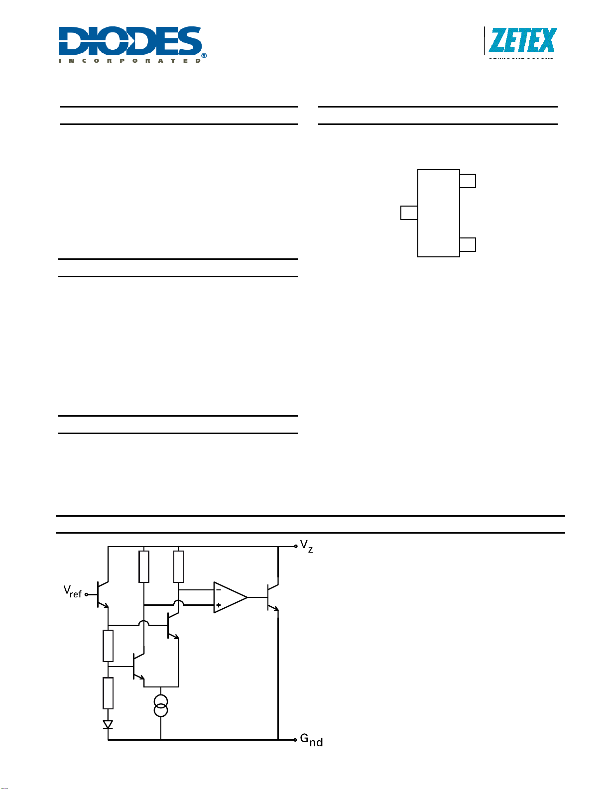
Pin Assignments
GND
SOT23
(Top View)
V
Z
V
REF
Typical Application Circuit
ZHT431
Document number: DS32157 Rev. 11 - 2
1 of 8
www.diodes.com
November 2010
© Diodes Incorporated
Page 2
A
Product Line o
f
f
Diodes Incorporated
Absolute Maximum Ratings (Voltages to GND Unless Otherwise Stated)
Parameter Rating Unit
V
Cathode Voltage (VZ)
20
Cathode Current 150 mA
Operating Temperature -55 to 125 °C
Storage Temperature -55 to 150 °C
Power Dissipation
(T
= 25°C, T
amb
JMAX
= 150°C)
330 mW
Recommended Operating Conditions
Parameter Min Max Units
Cathode Voltage V
REF
Cathode Current 0.05 100 mA
- 20 V
ZHT431
Electrical Characteristics (Test conditions unless otherwise specified: T
Symbol Parameter
V
REF
Reference Voltage 2%
1%
0.5%
V
DEV
ΔV
ΔV
I
REF
ΔI
REF
I
Zmin
I
Zof
RZ
REF
Deviation of reference input voltage
over temperature
Ratio of the change in reference voltage
to the change in cathode voltage
Z
Reference input current
Deviation of reference input current
over temperature
Minimum cathode current for regulation
Off-state current
Dynamic output impedance
Deviation of reference input voltage, V
, is defined as the maximum variation of the reference input voltage over the full
DEV
Min. Typ. Max.
2.45
2.475
2.4875
temperature range.
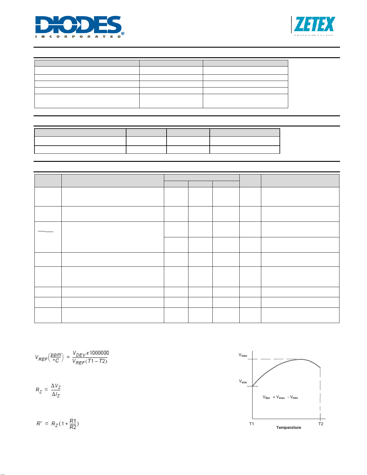
The average temperature coefficient of the reference input voltage, V
Values
2.50
2.50
2.50
2.55
2.525
2.5125
10 30 mV
-1.85 -2.7 mV/V
-1.0 -2. mV/V
0.12 1.0 µA
0.04 0.2 µA
35 50 µA
0.1 µA
0.75 V
is defined as:
REF
= 25°C)
amb
Units Conditions
I
=10mA (Fig.1),
L
V
V
Z=VREF
I
=10mA, VZ=V
L
=full range (Fig1)
T
amb
from V
V
Z
=10mA (Fig.2)
I
Z
VZ from 10V to 20V
=10mA (Fig.2)
I
Z
R1=10k, R2=O/C,
l
=10mA (Fig.2)
L
R1=10k, R2=O/C,
IL=10mA T
(Fig.2)
V
Z=VREF
=20V, V
V
Z
V
Z=VREF
=1mA to 100mA
I
C
REF
to 10V
REF
=full range
amb
(Fig.1)
=0V(Fig.3)
REF
(Fig.1), f=0Hz,
The dynamic output impedance, R
, is defined as:
Z
When the device is programmed with two external resistors, R1 and R2,
(fig 2) , the dynamic output impedance of the overall circuit, R’, is defined as:
ZHT431
Document number: DS32157 Rev. 11 - 2
2 of 8
www.diodes.com
November 2010
© Diodes Incorporated
Page 3
A
f
2
5
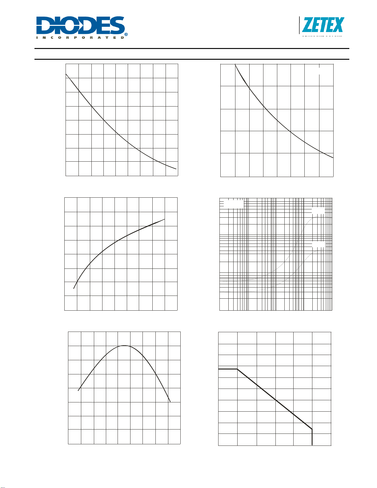
Typical Operating Conditions
170
160
150
Product Line o
Diodes Incorporated
ZHT431
0
I = 10mA
Z
-5
140
130
120
Reference Current (nA)
110
100
90
-50 125-25 10007525 50
40
38
36
34
32
30
28
Minimum Cathode Current (µA)
26
Temperature (°C)
I vs. Tempe rature
REF
-10
-15
-20
Change in Reference Output Voltage (mV)
-25
02015510
Change in V vs. Ca thode Voltage
100
V = V
REF Z
10
1.0
Dynamic Impedance ( )Ω
Cathode Voltage (V)
REF
1mA
10mA
24
-50 125-25 10007525 50
2.50
2.500
2.498
2.496
2.494
2.492
Reference Voltage (V)
2.490
2.488
2.486
-50 125-25 10007525 50
ZHT431
Document number: DS32157 Rev. 11 - 2
Temperature (°C)
I vs. Temperature
ZMIN
Temperature ( C)°
V vs. Temperature
REF
3 of 8
www.diodes.com
0.1
100 1K 10K 100K 1M
Dynamic Im pedance vs. Frequency
0.
0.4
0.3
0.2
Power Dissipation (W)
0.1
0
0
25 12550 10075
Frequency (Hz)
Ambient Temperature (°C)
Powe r Dissipation Derati n g
150
November 2010
© Diodes Incorporated
Page 4
A
f
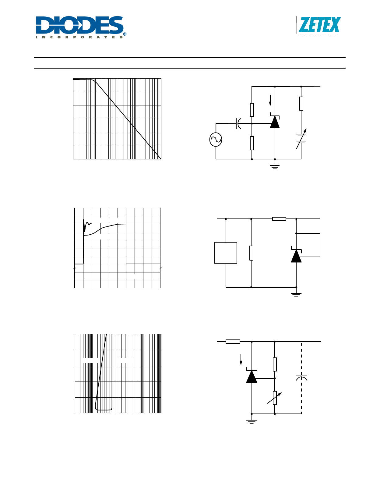
Typical Operating Conditions (Cont.)
Product Line o
Diodes Incorporated
ZHT431
60
)Bd(niaGegatloVpooLnepO
40
20
0
100 1k 10k 100k 1M
Frequency (Hz)
Gain v Frequency
3.0
)V(gniwSegatloV
2.0
1.0
0
5.0
0
Repetitive pulse
Single pulse
V
Z
INPUT
I
Z
15k
9μF
+
=10mA,
I
Z
8k25
T
A
=25°C
-
Test Circuit for Open Loop Voltage Gain
220
Input Monitor
Pulse
Generator
50
230
V
Z
V
Z
00.40.60.81.00.2
Time (µs)
Pulse Response
100
80
)Am(tnerruCedohtaC
60
40
20
0
10p
100p 1000p
STABLESTABLE
0.01µ0.1
Load Capacitance (F)
Stability Boundary Conditions
Test Circuit for Pulse Response
Input
µ
µ
1
V
ref<VZ
Test Circuit for Stability Boundary Conditions
TA=25°C
150
I
Z
10k
< 20, IZ=10mA,TA= 25°C
V
Z
ZHT431
Document number: DS32157 Rev. 11 - 2
4 of 8
www.diodes.com
November 2010
© Diodes Incorporated
Page 5
A
f
Z
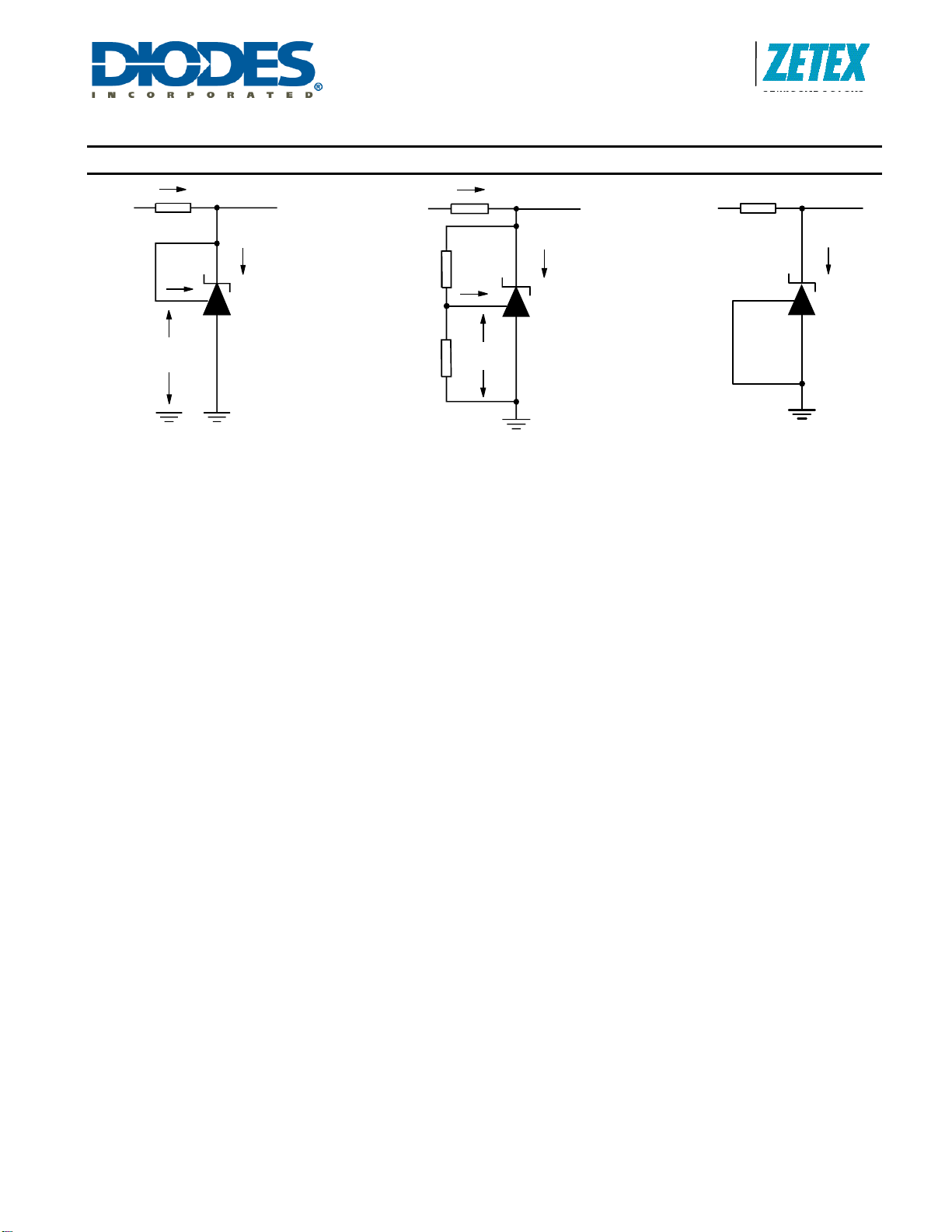
DC Test Circuits
Product Line o
Diodes Incorporated
ZHT431
I
Input Input Input
L
I
ref
V
ref
Fig 1 - Test circu it for VZ=V
V
Z
I
Z
R1
R2
ref
Fig 2 - Test circu it for VZ>V
I
L
I
ref
V
ref
V
Z
I
Z
ref
Fig 3 - Test circuit for
Off state current
I
ZOFF
†
V
ZHT431
Document number: DS32157 Rev. 11 - 2
5 of 8
www.diodes.com
November 2010
© Diodes Incorporated
Page 6
A
f
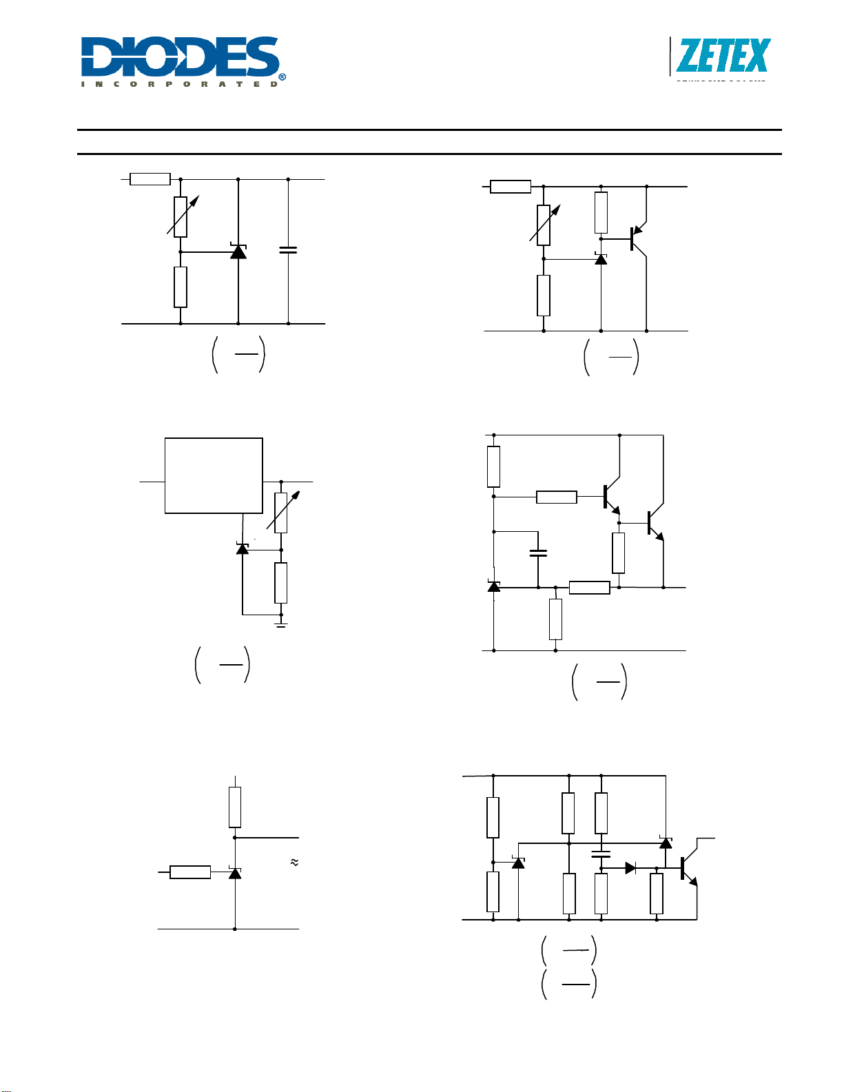
Application Circuits
V+Vout
Product Line o
Diodes Incorporated
ZHT431
V+Vout
R1
Vref
R2
R1
1+
Vout=
+
ZSR***
In
Common
Vout = Vref + Vreg
MIN
Vout= 1 +
R1
R2
R2
Out
Vref
Vout
R1
Vref
R2
Vref
Output control of a
three terminal fixed regulator
V+
Vref
Higher current shunt regulatorShunt regulator
Vref
Vout= 1 +
Series regulator
R1
R2
Vout=
30Ω
0.01µF
R2
R1
1+
R1
R2
R1
R2
Vref
Vout
Vref
6 of 8
V+
R1A
Vref
R2A
Low limit =
High limit =
R1B
R2B
1+
1+
R1B
R2B
R1A
R2A
Over voltage / under voltage
protection circuit
Vref
Vref
Vref
Output
November 2010
© Diodes Incorporated
V+
Output
2V
V
Input
V
TH
=2.5V
on
=V+
V
off
Single supply comparator
with temperature
compensated threshold
ZHT431
Document number: DS32157 Rev. 11 - 2
www.diodes.com
Page 7
A
Product Line o
f
Diodes Incorporated
ZHT431
Ordering Information
Ordering
Reference
ZHT431F01TA 1 1 SOT23 43C Active 7 3000 8mm
ZHT431F01-7 2 1 SOT23 43C Active 7 3000 8mm
ZHT431FMTA 1 0.5 SOT23 43P Active 7 3000 8mm
ZHT431F02TA 1 2 SOT23 43D Active 7 3000 8mm
Notes: 1. A ‘Green’ molding compound is used from date code 1010. For further details, refer to http://www.diodes.com/quality/lead_free.html
2. All date codes of the ‘-7’ option use ‘Green’ molding compound.
Tolerance
(%)
Package Part Mark Status
Reel Size
(inches)
Quantity
per reel
Tape
Width
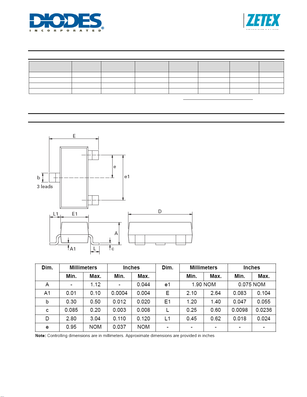
Package Outline Dimensions
SOT23
ZHT431
Document number: DS32157 Rev. 11 - 2
www.diodes.com
7 of 8
November 2010
© Diodes Incorporated
Page 8

A
Product Line o
f
Diodes Incorporated
ZHT431
DIODES INCORPORATED MAKES NO WARRANTY OF ANY KIND, EXPRESS OR IMPLIED, WITH REGARDS TO THIS DOCUMENT,
INCLUDING, BUT NOT LIMITED TO, THE IMPLIED WARRANTIES OF MERCHANTABILITY AND FITNESS FOR A PARTICULAR PURPOSE
(AND THEIR EQUIVALENTS UNDER THE LAWS OF ANY JURISDICTION).
Diodes Incorporated and its subsidiaries reserve the right to make modifications, enhancements, improvements, corrections or other changes
without further notice to this document and any product described herein. Diodes Incorporated does not assume any liability arising out of the
application or use of this document or any product described herein; neither does Diodes Incorporated convey any license under its patent or
trademark rights, nor the rights of others. Any Customer or user of this document or products described herein in such applications shall assume
all risks of such use and will agree to hold Diodes Incorporated and all the companies whose products are represented on Diodes Incorporated
website, harmless against all damages.
Diodes Incorporated does not warrant or accept any liability whatsoever in respect of any products purchased through unauthorized sales
channel.
Should Customers purchase or use Diodes Incorporated products for any unintended or unauthorized application, Customers shall indemnify and
hold Diodes Incorporated and its representatives harmless against all claims, damages, expenses, and attorney fees arising out of, directly or
indirectly, any claim of personal injury or death associated with such unintended or unauthorized application.
Products described herein may be covered by one or more United States, international or fo reign p atents pending. Product names a nd markings
noted herein may also be covered by one or more United States, international or foreign trademarks.
Diodes Incorporated products are specifically not authorized for use as critical components in life support devices or systems without the express
written approval of the Chief Executive Officer of Diodes Incorporated. As used herein:
A. Life support devices or systems are devices or systems which:
1. are intended to implant into the body, or
2. support or sustain life and whose failure to perform when properly used in accordance with instructions for use provided in the
labeling can be reasonably expected to result in significant injury to the user.
B. A critical component is any component in a life support device or system whose failure to perform can be reasonably expected to cause the
failure of the life support device or to affect its safety or effectiveness.
Customers represent that they have all necessary expertise in the safety and regulatory ramifications of their life support devices or systems, and
acknowledge and agree that they are solely responsible for all legal, regulatory and safety-related requirements concerning their products and
any use of Diodes Incorporated products in such safety-critical, life support devices or systems, notwithstanding any devices- or systems-related
information or support that may be provided by Diodes Incorporated. Further, Customers must fully indemnify Diodes Incorporated and its
representatives against any damages arising out of the use of Diodes Incorporated products in such safety-critical, life support devices or
systems.
Copyright © 2010, Diodes Incorporated
www.diodes.com
IMPORTANT NOTICE
LIFE SUPPORT
ZHT431
Document number: DS32157 Rev. 11 - 2
8 of 8
www.diodes.com
November 2010
© Diodes Incorporated
Page 9

 Loading...